

FEATURES
LTC4258
Quad IEEE 802.3af
Power over Ethernet Controller
with Integrated Detection
U
DESCRIPTIO
■
Controls Four Independent – 48V Powered
Ethernet Ports
■
Each Port Includes:
– IEEE 802
®
.3af Compliant PD Detection and
Classification
– Output Current Limit with Foldback
– Short-Circuit Protection with Fast Gate Pull-Down
– PD Disconnect Using DC Sensing
– Power Good Indication
■
Operates Autonomously or by I2C
■
4-Bit Programmable Digital Address Allows Control
TM
Control
of Up to 64 Ports
■
Programmable INT Pin Eliminates Software Polling
■
Current and Duty Cycle Limits Protect External FETs
■
Available in a 36-Pin SSOP Package
U
APPLICATIO S
■
IEEE 802.3af Compliant Endpoint and Midspan
Power Sources
■
IP Phone Systems
■
DTE Power Distribution
, LT, LTC and LTM are registered trademarks of Linear Technology Corporation.
Hot Swap is a registered trademark of Linear Technology Corporation.
All other trademarks are the property of their respective owners.
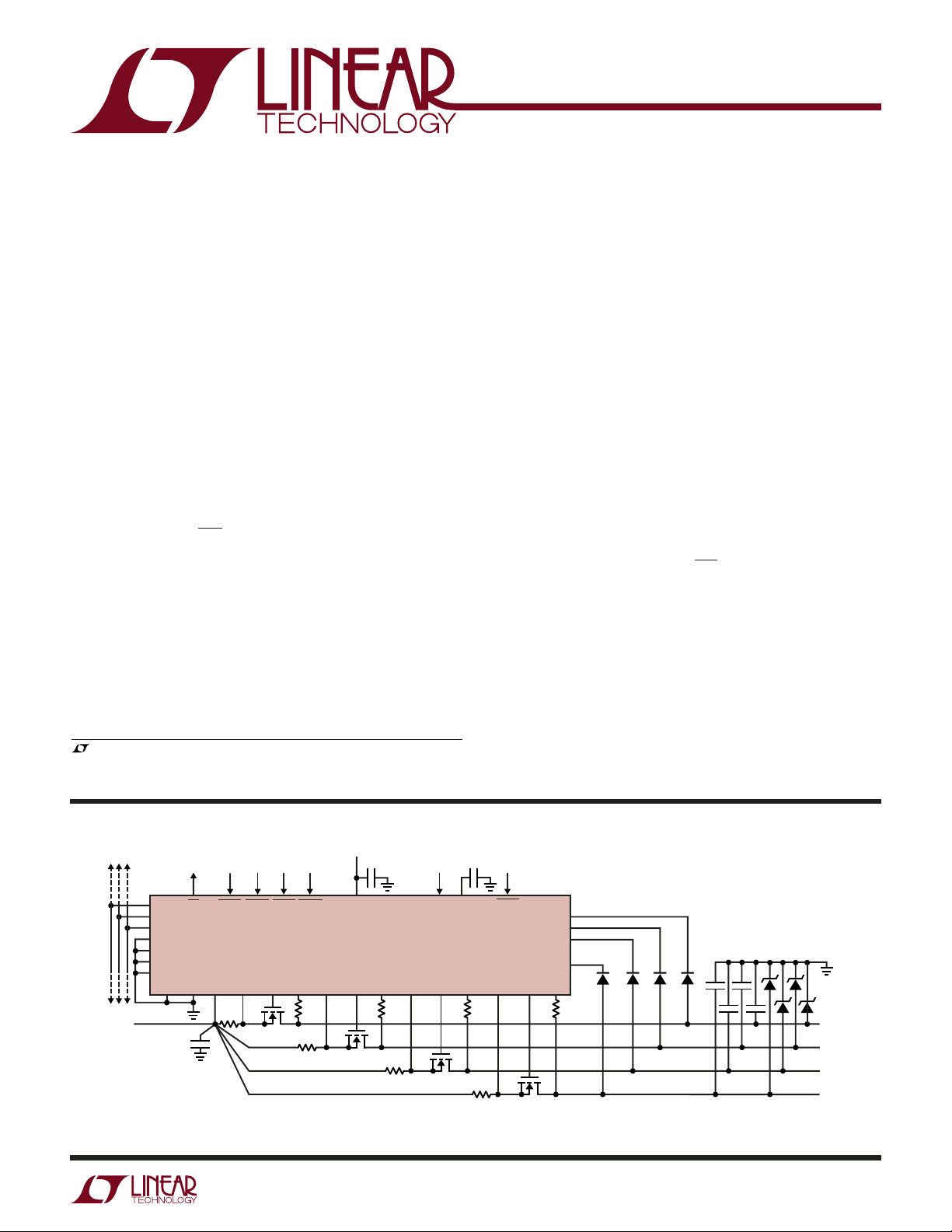
The LTC
®
4258 is a quad –48V Hot SwapTM controller designed for use in IEEE 802.3af compliant Power
Sourcing Equipment (PSE). It consists of four independent
ports, each with output current limit, short-circuit protection, complete Powered Device (PD) detection and classification capability, and programmable PD disconnect using
DC sensing. Used with power MOSFETs and passives as
in Figure 1, the LTC4258 can implement a complete IEEE
802.3af-compliant PSE.
The LTC4258 can operate autonomously or be controlled by
2
an I
C serial interface. Up to 16 LTC4258s may coexist on
the same data bus, allowing up to 64 powered Ethernet ports
to be controlled with only two digital lines. Fault conditions
are optionally signaled with the INT pin to eliminate software
polling.
External power MOSFETs, current sense resistors and diodes allow easy scaling of current and power dissipation
levels and provide protection against voltage and current
spikes and ESD events.
The LTC4258 is available in a 36-pin SSOP package.
Linear Technology also provides solutions for 802.3af PD
applications with the LTC4257, LTC4257-1, and LTC4267.
TYPICAL APPLICATIO
INT
SHDN1
SHDN2 SHDN3 SHDN4 V
V
EE
SENSE1
R
S1
RS1 TO RS4: 0.5Ω
Q1 TO Q4: IRFM120A
GATE1
Q1
OUT1 SENSE2 GATE2
–48V
SCL
SDAIN
SDAOUT
AD0
AD1
AD2
AD3
DGND
0.1µF
AGND
U
3.3V
0.1µF
DD
LTC4258
OUT2 SENSE3 GATE3 OUT3 SENSE4 GATE4 OUT4
10k
R
S2
10k 10k 10k
Q2
R
S3
Figure 1. Complete 4-Port Powered Ethernet Power Source
0.1µF
100V X7R
AUTO BYP RESET
Q3
R
S4
DETECT1
DETECT2
DETECT3
DETECT4
Q4
CMPD3003
×4
0.1µF 100V
×4
SMAJ58A
×4
4258 F01
PORT1
PORT2
PORT3
PORT4
4258fb
1
LTC4258
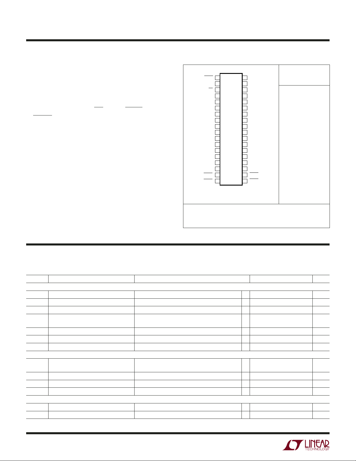
PACKAGE/ORDER I FOR ATIO
UU
W
1
2
3
4
5
6
7
8
9
10
11
12
13
14
15
16
17
18
TOP VIEW
GW PACKAGE
36-LEAD PLASTIC SSOP
36
35
34
33
32
31
30
29
28
27
26
25
24
23
22
21
20
19
RESET
BYP
INT
SCL
SDAOUT
SDAIN
AD3
AD2
AD1
AD0
DETECT1
DETECT2
DETECT3
DETECT4
DGND
V
DD
SHDN1
SHDN2
NC
AUTO
OUT1
GATE1
SENSE1
OUT2
GATE2
SENSE2
V
EE
OUT3
GATE3
SENSE3
OUT4
GATE4
SENSE4
AGND
SHDN4
SHDN3
WWWU
ABSOLUTE AXI U RATI GS
(Note 1)
Supply Voltages
to DGND .......................................... – 0.3V to 5V
V
DD
V
to AGND ......................................... 0.3V to – 70V
EE
DGND to AGND (Note 2) ................................. ±0.3V
Digital Pins
SCL, SDAIN, SDAOUT, INT, AUTO, RESET
n
, AD
SHDN
n .................
Analog Pins
GATE
n
(Note 3) ................... VEE – 0.3V to VEE + 12V
n
DETECT
SENSE
OUT
.................... DGND – 21V to DGND + 0.3V
n .................................
n ....................................
BYP Current ................................................. ±0.1mA
Operating Ambient Temperature Range ...... 0°C to 70°C
Junction Temperature (Note 4)............................ 150°C
Storage Temperature Range ................ –65°C to 150°C
Lead Temperature (Soldering, 10 sec)................. 300°C
DGND – 0.3V to DGND + 5V
VEE – 0.3V to VEE + 1V
VEE – 70V to VEE + 70V
ORDER PART
NUMBER
LTC4258CGW
T
= 150°C, θJA = 80°C/W
JMAX
Order Options Tape and Reel: Add #TR
Lead Free: Add #PBF Lead Free Tape and Reel: Add #TRPBF
Lead Free Part Marking: http://www.linear.com/leadfree/
Consult LTC Marketing for parts specified with wider operating temperature ranges.
ELECTRICAL CHARACTERISTICS
temperature range, otherwise specifications are at T
(Note 5).
SYMBOL PARAMETER CONDITIONS MIN TYP MAX UNITS
Power Supplies
V
DD
V
EE
I
DD
I
EE
V
DDMIN
V
EEMINONVEE
V
EEMINOFFVEE
Detection
I
DET
V
DET
R
DETMIN
R
DETMAX
Classification
V
CLASS
I
CLASS
2
VDD Supply Voltage
VEE Supply Voltage To Maintain IEEE Compliant Output (Note 6)
VDD Supply Current
VEE Supply Current Normal Operation
VDD UVLO Voltage 2.7 V
UVLO Voltage (Turning On) VEE – AGND –31 V
UVLO Voltage (Turning Off) VEE – AGND –28 V
Detection Current First Point, V
Detection Voltage Compliance Open Circuit, Measured at DETECTn Pin
Minimum Valid Signature Resistance
Maximum Valid Signature Resistance
Classification Voltage 0mA < I
Classification Current Compliance Into Short (V
The ● denotes the specifications which apply over the full operating
= 25°C. AGND = DGND = 0V, VDD = 3.3V, VEE = –48V unless otherwise noted
A
●
3 3.3 4 V
●
–47 –57 V
Classification Into a Short (V
= –10V
DETECT
Second Point, V
CLASS
DETECT
< 31mA
DETECT
n
n
= 0V)
= –3.5V
DETECT
= 0V) (Note 8)
n
●
●
●
●
235 300 µA
●
145 190 µA
●
●
15.2 17 19 kΩ
●
26.7 29 33 kΩ
●
–16.4 –21 V
●
55 75 mA
2.5 5 mA
–2 –5 mA
100 mA
–20 –23 V
4258fb

LTC4258
ELECTRICAL CHARACTERISTICS
temperature range, otherwise specifications are at T
The ● denotes the specifications which apply over the full operating
= 25°C. AGND = DGND = 0V, VDD = 3.3V, VEE = –48V unless otherwise noted
A
(Note 5).
SYMBOL PARAMETER CONDITIONS MIN TYP MAX UNITS
I
TCLASS
Gate Driver
I
GON
I
GOFF
I
GPD
∆V
GATE
Output Voltage Sense
V
PG
I
VOUT
Current Sense
V
CUT
V
LIM
V
MIN
V
SC
I
SENSE
Digital Interface
V
OLD
V
ILD
V
IHD
R
PU
R
PD
AC Characteristics
t
DETDLY
t
DET
t
CLSDLY
t
CLASS
t
PON
Classification Threshold Current Class 0-1
Class 1-2
Class 2-3
Class 3-4
Class 4-Overcurrent
GATE Pin Current Gate On, V
GATE Pin Current Gate Off, V
GATE Pin Short-Circuit Pull-Down V
External Gate Voltage (V
– VEE)I
GATE
n
Power Good Threshold Voltage V
Out Pin Bias Current 0V > V
Overcurrent Detection Sense Voltage V
Current Limit Sense Voltage V
DC Disconnect Sense Voltage V
= VEE + 2V 50 mA
GATE
n
= –1µA (Note 3)
GATE
n
– V
OUT
n
OUT
–10V > V
V
V
V
OUT
= –48V –20 µA
OUT
n
– VEE, V
SENSE
n
– VEE, V
SENSE
n
– VEE, V
SENSE
n
– VEE, V
SENSE
n
– V
SENSE
n
GATE
GATE
EE
> –10V
n
> –30V
n
EE
= V
n
EE
= VEE + 5V
n
= V
OUT
OUT
OUT
OUT
(Note 7) 166 187.5 199 mV
EE
= V
n
EE
= AGND – 30V 201 224 mV
n
= AGND – 10V 30.2 mV
n
●
5.5 6.5 7.5 mA
●
13 14.5 16 mA
●
21 23 25 mA
●
31 33 35 mA
●
45 48 51 mA
●
–20 –50 –70 µA
●
30 300 µA
●
10 13 15 V
●
123 V
●
●
–6 µA
–18 µA
201 212.5 224 mV
2.52 3.75 4.97 mV
Short-Circuit Sense Voltage 275 mV
SENSE Pin Bias Current V
Digital Output Low Voltage I
Digital Input Low Voltage SCL, SDAIN, RESET, SHDNn, AUTO, AD
Digital Input High Voltage SCL, SDAIN, RESET, SHDNn, AUTO, AD
Pull-Up Resistor to V
DD
= V
SENSE
n
EE
= 3mA, I
SDAOUT
I
SDAOUT
= 5mA, I
INT
INT
ADn, RESET, SHDN
= 3mA
= 5mA
n
–50 µA
●
●
n
n
●
●
2.4 V
0.4 V
0.7 V
0.8 V
50 kΩ
Pull-Down Resistor to DGND AUTO 50 kΩ
Detection Delay From Detect Command or Application of PD to Port
●
170 590 ms
to Detect Complete (Figure 2)
Detection Duration Time to Measure PD Signature Resistance (Figure 2)
Classification Delay From Successful Detect in Auto or Semiauto Mode
●
170 230 ms
●
10.1 52 ms
to Class Complete
●
From Classify Command in Manual Mode (Figure 2)
Classification Duration (Figure 2)
Power On Delay, Auto Mode From Valid Detect to Port On in Auto Mode (Figure 2)
From Port On Command to GATE Pin Current = I
GON
10.1 420 ms
●
10.1 13 ms
●
●
130 ms
1ms
(Note 9)
4258fb
3

LTC4258
ELECTRICAL CHARACTERISTICS
temperature range, otherwise specifications are at T
The ● denotes the specifications which apply over the full operating
= 25°C. AGND = DGND = 0V, VDD = 3.3V, VEE = –48V unless otherwise noted
A
(Note 5).
SYMBOL PARAMETER CONDITIONS MIN TYP MAX UNITS
t
START
t
ICUT
DC
CLMAX
t
DIS
t
VMIN
I2C Timing
f
SCLK
t
1
t
2
t
3
t
4
t
5
t
6
t
7
t
8
t
r
t
f
t
FLTINT
t
STOPINT
t
ARAINT
Maximum Current Limit Duration During t
Port Start-Up t
Maximum Current Limit Duration After t
Port Start-Up t
START1
START1
t
START1
t
START1
ICUT1
ICUT1
t
ICUT1
t
ICUT1
= 0, t
= 0, t
= 1, t
= 1, t
= 0, t
= 0, t
= 1, t
= 1, t
START0
START0
START0
START0
= 0 (Figure 3)
ICUT0
= 1 (Figure 3)
ICUT0
= 0 (Figure 3)
ICUT0
= 1 (Figure 3)
ICUT0
= 0 (Figure 3)
= 1 (Figure 3)
= 0 (Figure 3)
= 1 (Figure 3)
Maximum Current Limit Duty Cycle Reg16h = 00h
Disconnect Delay t
DC Disconnect Minimum Pulse V
DIS1
t
DIS1
t
DIS1
t
DIS1
SENSE
= 0, t
= 0, t
= 1, t
= 1, t
= 0 (Figure 4)
DIS0
= 1 (Figure 4)
DIS0
= 0 (Figure 4)
DIS0
= 1 (Figure 4)
DIS0
– VEE > 5mV, V
n
Width Sensitivity (Note 9)
Clock Frequency (Note 9)
Bus Free Time Figure 5 (Notes 9, 10)
Start Hold Time Figure 5 (Notes 9, 10)
SCL Low Time Figure 5 (Notes 9, 10)
SCL High Time Figure 5 (Notes 9, 10)
Data Hold Time Figure 5 (Notes 9, 10)
Data Set-Up Time Figure 5 (Notes 9, 10)
Start Set-Up Time Figure 5 (Notes 9, 10)
Stop Set-Up Time Figure 5 (Notes 9, 10)
SCL, SDAIN Rise Time Figure 5 (Notes 9, 10)
SCL, SDAIN Fall Time Figure 5 (Notes 9, 10)
Fault Present to INT Pin Low (Notes 9, 10, 11)
Stop Condition to INT Pin Low (Notes 9, 10, 11)
ARA to INT Pin High Time (Notes 9, 10)
= –48V (Figure 4)
OUT
n
●
50 60 70 ms
●
25 30 35 ms
●
100 120 140 ms
●
200 240 280 ms
●
50 60 70 ms
●
25 30 35 ms
●
100 120 140 ms
●
200 240 280 ms
●
5.8 6.3 6.7 %
●
300 360 400 ms
●
75 90 100 ms
●
150 180 200 ms
●
600 720 800 ms
●
●
●
1.3 µs
●
600 ns
●
1.3 µs
●
600 ns
●
150 ns
●
200 ns
●
600 ns
●
600 ns
●
20 300 ns
●
20 150 ns
●
20 150 ns
●
60 200 ns
●
20 300 ns
0.02 1 ms
400 kHz
Note 1: Stresses beyond those listed under Absolute Maximum Ratings
may cause permanent damage to the device. Exposure to any Absolute
Maximum Rating condition for extended periods may affect device
reliability and lifetime.
Note 2: DGND and AGND should be tied together in normal operation.
Note 3: An internal clamp limits the GATE pins to a minimum of 12V above
. Driving this pin beyond the clamp may damage the part.
V
EE
Note 4: This IC includes overtemperature protection that is intended to
protect the device during momentary overload conditions. Junction
temperature will exceed 125°C when overtemperature protection is active.
Continuous operation above the specified maximum operating junction
temperature may impair device reliability.
Note 5: All currents into device pins are positive; all currents out of device
4
pins are negative. All voltages are referenced to ground (AGND and DGND)
unless otherwise specified.
Note 6: The LTC4258 is designed to maintain a port voltage of –46.6V to
–57V. The V
supply voltage range accounts for the drop across the
EE
MOSFET and sense resistor.
Note 7: The LTC4258 implements overload current detection per IEEE
802.3af. The minimum overload current (I
voltage; I
CUT_MIN
= 15.4W/V
PORT_MIN
) is dependent on port
CUT
. An IEEE compliant system using the
LTC4258 should maintain port voltage above –46.6V.
Note 8: V
by measuring the DETECT
supply current while classifying a short is measured indirectly
EE
n
pin current while classifying a short.
Note 9: Guaranteed by design, not subject to test.
Note 10: Values measured at V
Note 11: If fault occurs during an I2C transaction, the INT pin will not be
pulled down until a stop condition is present on the I
ILD
and V
IHD
.
2
C bus.
4258fb
UW
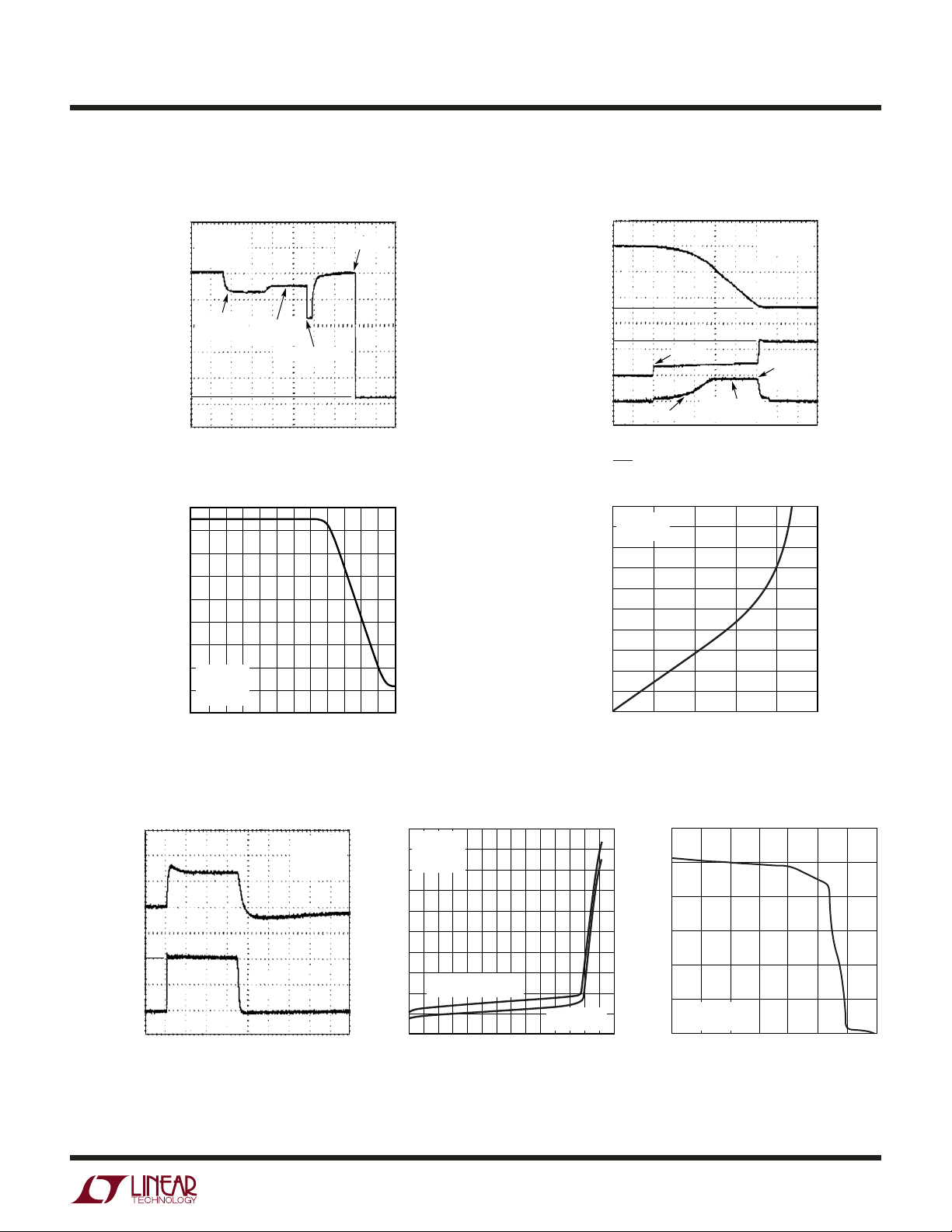
TYPICAL PERFOR A CE CHARACTERISTICS
LTC4258
PORT
VOLTAGE
10V/DIV
Power On Sequence in Auto Mode
GND
V
EE
PORT 1
= 3.3V
V
DD
= –48V
V
EE
DETECTION
PHASE 1
DETECTION
PHASE 2
CLASSIFICATION
50ms/DIV
POWER ON
Current Limit Foldback
225
200
175
150
125
(mV)
n
100
SENSE
V
75
50
VDD = 3.3V
= –48V
V
EE
25
= 25°C
T
A
0
–48 0
–40
–24–32 –16 –8
V
OUTn-AGND
(V)
4258 G01
4258 G03
450
400
350
300
250
200
150
100
50
0
I
LIMIT
WITH R
SENSE
= 0.5Ω (mA)
PORT
VOLTAGE
20V/DIV
GATE
VOLTAGE
10V/DIV
PORT
CURRENT
500mA/DIV
Powering On a 180µF Load
GND
V
EE
V
EE
+14V
V
0mA
EE
FET ON
FOLDBACK
CURRENT LIMIT
5ms/DIV
INT and SDAOUT Pull Down
Voltage vs Load Current
2.0
VDD = 3.3V
1.8
= 25°C
T
A
1.6
1.4
1.2
1.0
0.8
0.6
PULL-DOWN VOLTAGE (V)
0.4
0.2
0
5
0
10
LOAD CURRENT (mA)
425mA
15
VDD = 3.3V
= –48V
V
EE
LOAD
FULLY
CHARGED
4258 G02
20
4258 G06
25
PORT
VOLTAGE
1V/DIV
PORT
CURRENT
20mA/DIV
Classification Transient Response
to 40mA Load Step Classification Current Compliance
0
VDD = 3.3V
–2
= –48V
V
EE
= 25°C
T
A
–4
–6
–8
–10
–12
–14
PORT VOLTAGE WITH
TYPICAL CMPD3003
–16
CLASSIFICATION VOLTAGE (V)
–18
–20
0 10203040506070
CLASSIFICATION CURRENT (mA)
PIN VOLTAGE
–18V
40mA
0mA
50µs/DIV
VDD = 3.3V
= –48V
V
EE
= 25°C
T
A
4258 G07
DETECT
n
4258 G08
VEE DC Supply Current vs
Supply Voltage
3.0
2.5
2.0
1.5
1.0
SUPPLY CURRENT (mA)
0.5
VDD = 3.3V
REG 12h = 00h
0
–70
–60 –50
–40 –20
VEE SUPPLY VOLTAGE (V)
–30 –10 0
4258 G09
4258fb
5
LTC4258
WU
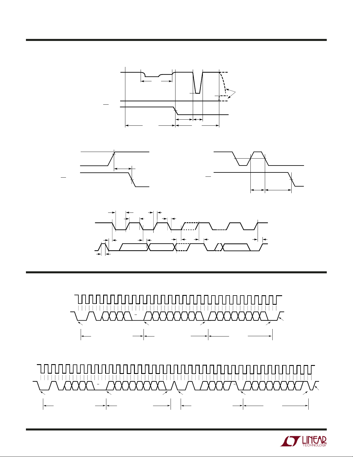
TEST TI I G
PORT
n
PD
INSERTED
0VV
t
DET
V
SENSE
PORT
TURN ON
(AUTO MODE)
V
GATE
V
CLASS
V
n
EE
V
T
INT
t
DETDLY
t
CLSDLY
t
PON
t
CLASS
4258 F02
Figure 2. Detect, Class and Turn-On Timing in Auto or Semiauto Modes
V
TO V
n
LIM
EE
0V
INT
V
CUT
t
START
, t
ICUT
V
SENSE
TO V
n
V
EE
MIN
INT
t
4258 F03
VMIN
Figure 3. Current Limit Timing Figure 4. DC Disconnect Timing
SCL
SDA
t
3
t
4
t
2
t
1
t
r
t
f
t
5
t
6
t
7
t
8
4258 F05
Figure 5. I2C Interface Timing
t
DIS
4258 F04
WUW
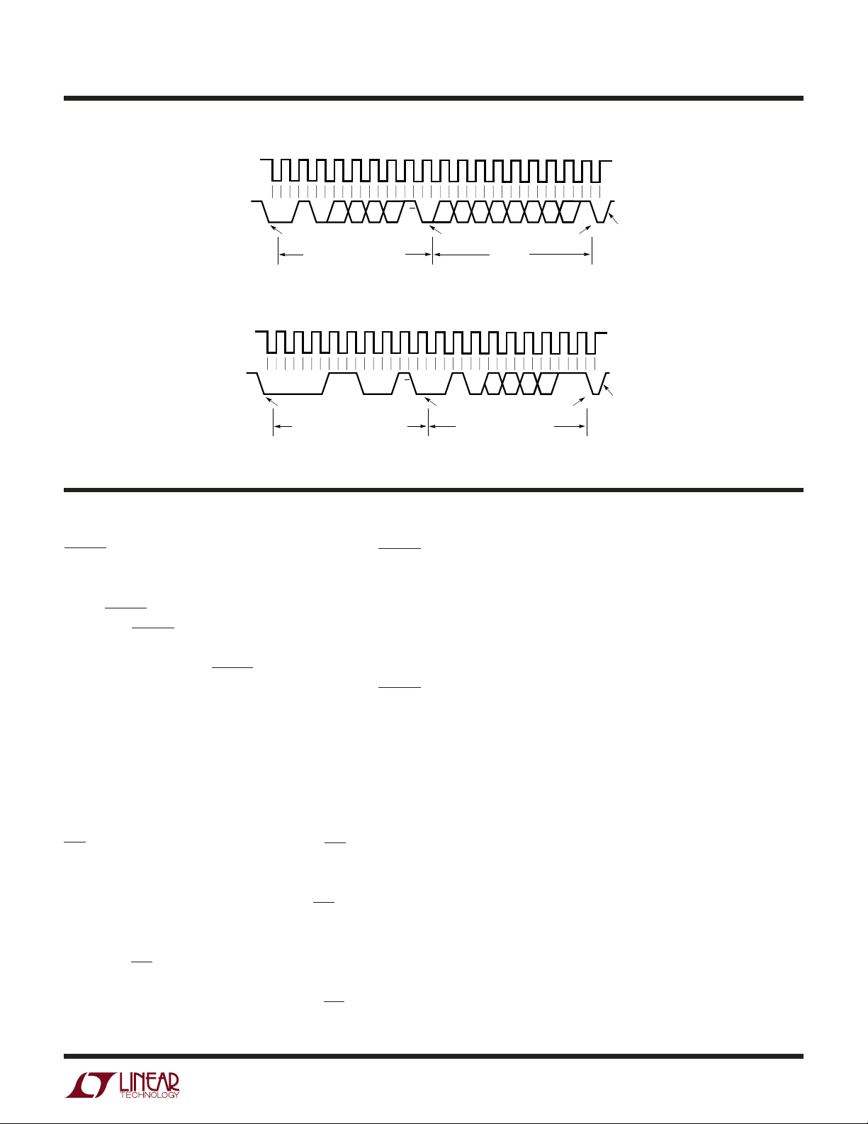
TI I G DIAGRA S
SCL
SCL
SDA
SDA
001
START BY
MASTER
AD3 AD2 AD1 AD0 A7 A6 A5 A4 A3 A2 A1 A0
SERIAL BUS ADDRESS BYTE
FRAME 1
001
START BY
MASTER
AD3 AD2 AD1 AD0 A7 A6 A5 A4 A3 A2 A1 A0
SERIAL BUS ADDRESS BYTE
ACK
R/W
6
FRAME 1
ACK BY
SLAVE
REGISTER ADDRESS BYTE
ACK
R/W
ACK BY
SLAVE
FRAME 2
REGISTER ADDRESS BYTE
ACK BY
SLAVE
Figure 6. Writing to a Register
ACK
001
REPEATED
START BY
MASTER
SERIAL BUS ADDRESS BYTE
FRAME 2
ACK BY
SLAVE
Figure 7. Reading from a Register
ACK ACK
D7 D6 D5 D4 D3 D2 D1 D0
4258 F06
FRAME 2
DATA BYTE
STOP BY
MASTER
NO ACK BY
MASTER
ACK BY
SLAVE
FRAME 3
DATA BYTE
AD3 AD2 AD1 AD0 D7 D6 D5 D4 D3 D2 D1 D0
FRAME 1
R/W
ACK
ACK BY
SLAVE
ACK
4258 F07
STOP BY
MASTER
4258fb
WUW
TI I G DIAGRA S
SCL
LTC4258
SDA
01
START BY
MASTER
AD3 AD2 AD1 AD0 D7 D6 D5 D4 D3 D2 D1 D0
0
SERIAL BUS ADDRESS BYTE
FRAME 1
R/W
ACK
Figure 8. Reading the Interrupt Register (Short Form)
SCL
SDA
00 11
0
START BY
MASTER
FRAME 1
ALERT RESPONSE ADDRESS BYTE
R/W
ACK
Figure 9. Reading from Alert Response Address
U
UU
PI FU CTIO S
RESET (Pin 1): Chip Reset, Active Low. When the RESET
pin is low, the LTC4258 is held inactive with all ports off
and all internal registers reset to their power-up states.
When RESET is pulled high, the LTC4258 begins normal
operation. RESET can be connected to an external capacitor or RC network to provide a power turn-on delay.
Internal filtering of the RESET pin prevents glitches less
than 1µs wide from resetting the LTC4258. Pull RESET
high with ≤10k or tie to V
BYP (Pin 2): Bypass Output. The BYP pin is used to
connect the internally generated –20V supply to an external 0.1µF bypass capacitor. Use a 100V rated 0.1µF, X7R
capacitor. Do not connect the BYP pin to any other external
circuitry.
INT (Pin 3): Interrupt Output, Open Drain. INT will pull low
when any one of several events occur in the LTC4258. It
will return to a high impedance state when bits 6 or 7 are
set in the Reset PB register (1Ah). The INT signal can be
used to generate an interrupt to the host processor,
eliminating the need for continuous software polling.
Individual INT events can be disabled using the Int Mask
register (01h). See Register Functions and Applications
Information for more information. The INT pin is only
2
updated between I
C transactions.
DD
.
ACK
ACK BY
SLAVE
ACK BY
SLAVE
FRAME 2
DATA BYTE
AD30000 1 AD2 AD1 AD0
FRAME 2
SERIAL BUS ADDRESS BYTE
NO ACK BY
MASTER
NO ACK BY
MASTER
STOP BY
MASTER
4258 F08
ACK1
STOP BY
MASTER
4258 F09
SCL (Pin 4): Serial Clock Input. High impedance clock
input for the I
be connected directly to the I
2
C serial interface bus. The SCL pin should
2
C SCL bus line.
SDAOUT (Pin 5): Serial Data Output, Open Drain Data
Output for the I
2
C Serial Interface Bus. The LTC4258 uses
two pins to implement the bidirectional SDA function to
2
simplify optoisolation of the I
C bus. To implement a standard bidirectional SDA pin, tie SDAOUT and SDAIN together.
See Applications Information for more information.
SDAIN (Pin 6): Serial Data Input. High impedance data input
2
for the I
C serial interface bus. The LTC4258 uses two pins
to implement the bidirectional SDA function to simplify
optoisolation of the I
2
C bus. To implement a standard
bidirectional SDA pin, tie SDAOUT and SDAIN together.
See Applications Information for more information.
AD3 (Pin 7): Address Bit 3. Tie the address pins high or low
2
to set the I
sponds. This address will be (010A
C serial address to which the LTC4258 re-
3A2A1A0)b
. Pull AD3
high or low with ≤10k or tie to VDD or DGND.
AD2 (Pin 8): Address Bit 2. See AD3.
AD1 (Pin 9): Address Bit 1. See AD3.
AD0 (Pin 10): Address Bit 0. See AD3.
4258fb
7

LTC4258
U
UU
PI FU CTIO S
DETECT1 (Pin 11): Detect Sense, Port 1. The LTC4258
Powered Device (PD) detection and classification hardware monitors port 1 with this pin. Connect DETECT1 to
the output port via a low leakage diode (see Figure 1). If the
port is unused, the DETECT1 pin can be tied to AGND or
allowed to float.
DETECT2 (Pin 12): Detection Sense, Port 2. See DETECT1.
DETECT3 (Pin 13): Detection Sense, Port 3. See DETECT1.
DETECT4 (Pin 14): Detection Sense, Port 4. See DETECT1.
DGND (Pin 15): Digital Ground. DGND should be con-
nected to the return from the 3.3V supply. DGND and
AGND should be tied together.
V
(Pin 16): Logic Power Supply. Connect to a 3.3V
DD
power supply relative to DGND. VDD must be bypassed to
DGND near the LTC4258 with at least a 0.1µF capacitor.
SHDN1 (Pin 17): Shutdown Port 1, Active Low. When
pulled low, SHDN1 shuts down port 1, regardless of the
state of the internal registers. Pulling SHDN1 low is
equivalent to setting the Reset Port 1 bit in the Reset
Pushbutton register (1Ah). Internal filtering of the SHDN1
pin prevents glitches less than 1µs wide from reseting the
LTC4258. Pull SHDN1 high with ≤10k or tie to V
SHDN2 (Pin 18): Shutdown Port 2, Active Low. See
SHDN1.
DD
.
GATE4 (Pin 23): Port 4 Gate Drive. GATE4 should be
connected to the gate of the external MOSFET for port 4.
When the MOSFET is turned on, a 50µA pull-up current
source is connected to the pin. The gate voltage is clamped
to 13V (typ) above V
the voltage at GATE4 will be reduced to maintain constant
current through the external MOSFET. If the fault timer
expires, GATE4 is pulled down with 50µA, turning the
MOSFET off and recording a t
port is unused, float the GATE4 pin or tie it to V
OUT4 (Pin 24): Port 4 Output Voltage Monitor. OUT4
should be connected to the output port through a 10k
series resistor. A current limit foldback circuit limits the
power dissipation in the external MOSFET by reducing the
current limit threshold when the port voltage is within 18V
of AGND. The port 4 Power Good bit is set when the voltage
from OUT4 to V
is connected internally from OUT4 to AGND. If the port is
unused, the OUT4 pin can be tied to AGND or allowed to
float.
SENSE3 (Pin 25): Port 3 Current Sense Input. See SENSE4.
GATE3 (Pin 26): Port 3 Gate Drive. See GATE4.
OUT3 (Pin 27): Port 3 Output Voltage Monitor. See OUT4.
(Pin 28): –48V Supply Input. Connect to a –48V to
V
EE
–57V supply, relative to AGND.
EE
. During a current limit condition,
EE
or t
ICUT
drops below 2V (typ). A 2.5MΩ resistor
event. If the
START
EE
.
SHDN3 (Pin 19): Shutdown Port 3, Active Low. See
SHDN1.
SHDN4 (Pin 20): Shutdown Port 4, Active Low. See
SHDN1.
AGND (Pin 21): Analog Ground. AGND should be connected to the return from the – 48V supply. AGND and
DGND should be tied together.
SENSE4 (Pin 22): Port 4 Current Sense Input. SENSE4
monitors the external MOSFET current via a 0.5Ω sense
resistor between SENSE4 and V
across the sense resistor exceeds the overcurrent detection threshold V
If the voltage across the sense resistor reaches the current
limit threshold V
GATE4 pin voltage is lowered to maintain constant current
in the external MOSFET. See Applications Information for
further details. If the port is unused, the SENSE4 pin must
be tied to VEE.
, the current limit fault timer counts up.
CUT
(typically 25mV/50mA higher), the
LIM
. Whenever the voltage
EE
SENSE2 (Pin 29): Port 2 Current Sense Input. See SENSE4.
GATE2 (Pin 30): Port 2 Gate Drive. See GATE4.
OUT2 (Pin 31): Port 2 Output Voltage Monitor. See OUT4.
SENSE1 (Pin 32): Port 1 Current Sense Input. See SENSE4.
GATE1 (Pin 33): Port 1 Gate Drive. See GATE 4.
OUT1 (Pin 34): Port 1 Output Voltage Monitor. See OUT4.
AUTO (Pin 35): Auto Mode Input. Auto mode allows the
LTC4258 to detect and power up a PD even if there is no
host controller present on the I2C bus. The voltage of the
AUTO pin determines the state of the internal registers
when the LTC4258 is reset or comes out of V
the Register map in Table 1). The states of these register
bits can subsequently be changed via the I
The real-time state of the AUTO pin is read at bit 0 in the
Pin Status register (11h). Pull AUTO high or low with ≤10k
or tie to V
NC (Pin 36): No Internal Connection.
or DGND.
DD
UVLO (see
DD
2
C interface.
4258fb
8

W
TABLE 1. REGISTER AP
Fault 1 0000,0000 0000,0000
Fault 1 0000,0000 0000,0000
ICUT
START
Fault 2 t
Fault 2 t
ICUT
START
Fault 3 t
Fault 3 t
ICUT
START
01
0
A
1
,A
2
A
3
00 00A
0
A
1
,A
2
A
3
0000,0000 0000,0000
DIS0
t
DIS1
t
ICUT0
t
LTC4258
UVLO
EE
supplies are brought up.
EE
UVLO is not set by RESET pin or
and V
DD
DD
reset all pushbutton.
V
V
bit depends on the order in which the
* The start-up state of the V
WO = Write Only
CoR = Clear on Read
R/W = Read/Write
RO = Read Only
Key:
Fault Class Complete Detect Complete Disconnect Pwr Good Event Pwr Enable Event 1000,0000 1000,0000
ICUT
Fault t
START
Fault 4 t
ICUT
Fault 4 t
START
UVLO Reserved Reserved Reserved Reserved 0011,0000* 0011,0000*
EE
UVLO V
DD
ICUT1
t
START0
t
START1
Enable
Interrupts
00h Interrupt RO Global Supply Event t
Interrupts Auto Pin Low Auto Pin High
ADDRESS REGISTER NAME R/W PORT BIT 7 BIT 6 BIT 5 BIT 4 BIT 3 BIT 2 BIT 1 BIT 0 RESET STATE RESET STATE
02h Power Event RO 4321 Pwr Good Pwr Good Pwr Good Pwr Good Pwr Enable Pwr Enable Pwr Enable Pwr Enable 0000,0000 0000,0000
01h Int Mask R/W Global Mask 7 Mask 6 Mask 5 Mask 4 Mask 3 Mask 2 Mask 1 Mask 0 1000,0000 1110,0100
Events
04h Detect Event RO 4321 Class Complete 4 Class Complete 3 Class Complete 2 Class Complete 1 Detect Complete 4 Detect Complete 3 Detect Complete 2 Detect Complete 1 0000,0000 0000,0000
03h Power Event CoR CoR Change 4 Change 3 Change 2 Change 1 Change 4 Change 3 Change 2 Change 1
05h Detect Event CoR CoR
Event CoR CoR
Event RO 4321 Reserved Reserved Reserved Reserved t
START
START
111 Overcurrent 111 Reserved
110 Class 0 110 Open Circuit
101 Undefined—Read as Class 0 101 RHIGH
100 Class 4 100 Detect Good
011 Class 3 011 RLOW 11 Auto Detect, Class and Power Automatically
010 Class 2 010 Reserved 10 Semiauto Detect and Class But Wait to Turn On Power
001 Class 1 001 Short Circuit (<1V) 01 Manual Will Not Advance Between States
0Fh Port 4 Status RO 4 Reserved Class Status 2 Class Status 1 Class Status 0 Reserved Detect Status 2 Detect Status 1 Detect Status 0 0000,0000 0000,0000
11h Pin Status RO Global Reserved Reserved AD3 Pin Status AD2 Pin Status AD1 Pin Status AD0 Pin Status Reserved Auto Pin Status 00A
10h Power Status RO 4321 Power Good 4 Power Good 3 Power Good 2 Power Good 1 Power Enable 4 Power Enable 3 Power Enable 2 Power Enable 1 0000,0000 0000,0000
06h Fault Event RO 4321 Disconnect 4 Disconnect 3 Disconnect 2 Disconnect 1 t
0Bh Supply Event CoR CoR
0Ah Supply Event RO 4321 Over Temp Reserved V
Status
09h t
08h t
07h Fault Event CoR CoR
0Eh Port 3 Status RO 3 Reserved Class Status 2 Class Status 1 Class Status 0 Reserved Detect Status 2 Detect Status 1 Detect Status 0 0000,0000 0000,0000
0Ch Port 1 Status RO 1 Reserved Class Status 2 Class Status 1 Class Status 0 Reserved Detect Status 2 Detect Status 1 Detect Status 0 0000,0000 0000,0000
0Dh Port 2 Status RO 2 Reserved Class Status 2 Class Status 1 Class Status 0 Reserved Detect Status 2 Detect Status 1 Detect Status 0 0000,0000 0000,0000
Configuration
13h Disconnect Enable R/W 4321 Reserved Reserved Reserved Reserved DC Discon En 4 DC Discon En 3 DC Discon En 2 DC Discon En 1 0000,0000 0000,1111
12h Operating Mode R/W 4321 Port 4 Mode 1 Port 4 Mode 0 Port 3 Mode 1 Port 3 Mode 0 Port 2 Mode 1 Port 2 Mode 0 Port 1 Mode 1 Port 1 Mode 0 0000,0000 1111,1111
14h Detect/Class Enable R/W 4321 Class Enable 4 Class Enable 3 Class Enable 2 Class Enable 1 Detect Enable 4 Detect Enable 3 Detect Enable 2 Detect Enable 1 0000,0000 1111,1111
16h Timing Config R/W Global Reserved Reserved t
15h Reserved R/W Reserved Reserved Reserved Reserved Reserved Reserved Reserved Reserved 0000,0000 0000,0000
17h Misc Config R/W Global Interrupt Pin Reserved Reserved Reserved Reserved Reserved Reserved Reserved 1000,0000 1000,0000
19h Power Enable PB WO 4321 Power Off 4 Power Off 3 Power Off 2 Power Off 1 Power On 4 Power On 3 Power On 2 Power On 1 0000,0000 0000,0000
18h Det/Class Restart PB WO 4321 Restart Class 4 Restart Class 3 Restart Class 2 Restart Class 1 Restart Detect 4 Restart Detect 3 Restart Detect 2 Restart Detect 1 0000,0000 0000,0000
Pushbuttons
1Ah Reset PB WO Global Clear All Clear Interrupt Pin Reserved Reset All Reset Port 4 Reset Port 3 Reset Port 2 Reset Port 1 0000,0000 0000,0000
000 Class Status Unknown 000 Detect Status Unknown 00 Shutdown Power Off, Detection and Class Off
CLASS STATUS DETECT STATUS MODE BIT ENCODING
Encoding
4258fb
9

LTC4258
UU
REGISTER FU CTIO S
Interrupt Registers
Interrupt (Address 00h): Interrupt Register, Read Only. A
transition to logical 1 of any bit in this register will assert
the INT pin (Pin 3) if the corresponding bit in the Int Mask
register is set. Each bit is the logical OR of the corresponding bits in the Event registers. The Interrupt register is Read
Only and its bits cannot be cleared directly. To clear a bit
in the Interrupt register, clear the corresponding bits in the
appropriate Status or Event registers or set bit 7 in the Reset
Pushbutton register (1Ah).
Int Mask (Address 01h): Interrupt Mask, Read/Write. A logic
1 in any bit of the Int Mask register allows the corresponding Interrupt register bit to assert the INT pin if it is set. A
logic 0 in any bit of the Int Mask register prevents the corresponding Interrupt bit from affecting the INT pin. The
actual Interrupt register bits are unaffected by the state of
the Int Mask register.
Event Registers
Power Event (Address 02h): Power Event Register, Read
Only. The lower four bits in this register indicate that the
corresponding port Power Enable status bit has changed;
the logical OR of these four bits appears in the Interrupt
register as the Pwr Enable Event bit. The upper four bits
indicate that the corresponding port Power Good status bit
has changed; the logical OR of these four bits appears in
the Interrupt register as the Pwr Good Event bit. The Power
Event bits latch high and will remain high until cleared by
reading from address 03h.
Power Event CoR (Address 03h): Power Event Register,
Clear on Read. Read this address to clear the Power Event
register. Address 03h returns the same data as address 02h
and reading address 03h clears all bits at both addresses.
Detect Event (Address 04h): Detect Event Register, Read
Only. The lower four bits in this register indicate that at least
one detection cycle for the corresponding port has completed; the logical OR of these four bits appears in the Interrupt register as the Detect Complete bit. The upper four
bits indicate that at least one classification cycle for the
corresponding port has completed; the logical OR of these
four bits appears in the Interrupt register as the Class Complete bit. In Manual mode, this register indicates that the
requested detection/classification cycle has completed and
the LTC4258 is awaiting further instructions. In Semiauto
or Auto modes, these bits indicate that the Detect Status
and Class Status bits in the Port Status registers are valid.
The Detect Event bits latch high and will remain high until
cleared by reading from address 05h.
Detect Event CoR (Address 05h): Detect Event Register,
Clear on Read. Read this address to clear the Detect Event
register. Address 05h returns the same data as address 04h,
and reading address 05h clears all bits at both addresses.
Fault Event (Address 06h): Fault Event Register, Read Only.
The lower four bits in this register indicate that a
t
fault has occurred at the corresponding port; the logi-
ICUT
cal OR of these four bits appears in the Interrupt register
as the t
connect event has occurred at the corresponding port; the
logical OR of these four bits appears in the Interrupt register as the Disconnect bit. The Fault Event bits latch high
and will remain high until cleared by reading from address
07h.
Fault Event CoR (Address 07h): Fault Event Register, Clear
on Read. Read this address to clear the Fault Event register. Address 07h returns the same data as address 06h and
reading address 07h clears all bits at both addresses.
t
START
Only. The lower four bits in this register indicate that a t
fault has occurred at the corresponding port; the logical OR
of these four bits appears in the Interrupt register as the
t
START
remain high until cleared by reading from address 09h. The
upper four bits in this register are reserved and will always
read as 0.
t
START
Clear on Read. Read this address to clear the Fault Event
register. Address 09h returns the same data as address 08h
and reading address 09h clears all bits at both addresses.
Supply Event (Address 0Ah): Supply Event Register, Read
Only. Bit 4 indicates that V
UVLO level (typically – 28V). Bit 5 signals that the VDD supply
has dropped below the V
that the LTC4258 die temperature has exceeded its thermal
shutdown limit (see Note 4 under Electrical Characteristics). The logical OR of bits 4, 5 and 7 appears in the Interrupt register as the Supply Fault bit. The remaining bits in
Fault bit. The upper four bits indicate that a Dis-
ICUT
Event (Address 08h): t
Fault bit. The t
Event CoR (Address 09h): t
Event bits latch high and will
START
EE
UVLO threshold. Bit 7 indicates
DD
Event Register, Read
START
Event Register,
START
has dropped below the V
START
EE
4258fb
10

UU
REGISTER FU CTIO S
LTC4258
the register are reserved and will always read as 0. The
Supply Event bits latch high and will remain high until
cleared by reading from address 0Bh.
Supply Event CoR (Address 0Bh): Supply Event Register,
Clear on Read. Read this address to clear the Fault Event
register. Address 0Bh returns the same data as address 0Ah,
and reading address 0Bh clears all bits at both addresses.
Status Registers
Port 1 Status (Address 0Ch): Port 1 Status Register, Read
Only. This register reports the most recent detection and
classification results for port 1. Bits 0-2 report the status
of the most recent detection attempt at the port and bits 4-6
report the status of the most recent classification attempt
at the port. If power is on, these bits report the detection/
classification status present just before power was turned
on. If power is turned off at the port for any reason, all bits
in this register will be cleared. See Table 1 for detection and
classification status bit encoding.
Port 2 Status (Address 0Dh): Port 2 Status Register, Read
Only. See Port 1 Status.
Port 3 Status (Address 0Eh): Port 3 Status Register, Read
Only. See Port 1 Status.
Port 4 Status (Address 0Fh): Port 4 Status Register, Read
Only. See Port 1 Status.
Power Status (Address 10h): Power Status Register, Read
Only. The lower four bits in this register report the switch
on/off state for the corresponding ports. The upper four
bits (the power good bits) indicate that the drop across the
power switch and sense resistor for the corresponding ports
is less than 2V (typ) and power start-up is complete. The
power good bits are latched high and are only cleared when
a port is turned off or the LTC4258 is reset.
Pin Status (Address 11h): External Pin Status, Read Only.
This register reports the real time status of the AUTO
(Pin 35) and AD0-AD3 (Pins 7-10) digital input pins. The
logic state of the AUTO pin appears at bit 0 and the AD0-AD3
pins at bits 2-5. The remaining bits are reserved and will
read as 0. AUTO affects the initial states of some of the
LTC4258 configuration registers at start-up but has no
effect after start-up and can be used as a general purpose
input if desired, as long as it is guaranteed to be in the
appropriate state at start-up.
Configuration Registers
Operating Mode (Address 12h): Operating Mode Configu-
ration, Read/Write. This register contains the mode bits for
each of the four ports in the LTC4258. See Table 1 for mode
bit encoding. At power-up, all bits in this register will be set
to the logic state of the AUTO pin (Pin 35). See Operating
Modes in the Applications Information section.
Disconnect Enable (Address 13h): Disconnect Enable
Register, Read/Write. The lower four bits of this register
enable or disable DC disconnect detection circuitry at the
corresponding port. If the DC Discon Enable bit is set the
port circuitry will turn off power if the current draw at the
port falls below I
, where RS is the sense resistor and should be 0.5Ω for
R
S
for more than t
MIN
DIS
. I
is equal to V
MIN
MIN
/
IEEE 802.3af compliance. If the bit is clear the port will not
remove power due to low current.
Detect/Class Enable (Address 14h): Detection and Classification Enable, Read/Write. The lower four bits of this register enable the detection circuitry at the corresponding port
if that port is in Auto or Semiauto mode. The upper four bits
enable the classification circuitry at the corresponding port
if that port is in Auto or Semiauto mode. In manual mode,
setting a bit in this register will cause the LTC4258 to perform one classification or detection cycle on the corresponding port. Writing to the Detect/Class Restart PB (18h)
has the same effect without disturbing the Detect/Class
Enable bits for other ports.
Timing Config (Address 16h): Global Timing Configuration,
Read/Write. Bits 0-1 program t
, the time duration before
DIS
a port is automatically tuned off after the PD is removed.
Bits 2-3 program t
current can exceed I
current is still above I
dicate a t
t
START
fault and turn the port off. Bits 4-5 program
ICUT
, the time duration before an overcurrent condition
during port power-on is considered a t
port is turned off. Note that using the t
, the time during which a port’s
ICUT
without it being turned off. If the
CUT
CUT
after t
, the LTC4258 will in-
ICUT
fault and the
START
and t
ICUT
START
times
other than the default is not compliant with IEEE 802.3af
and may double or quadruple the energy dissipated by the
external MOSFETs during fault conditions. Bits 6-7 are reserved and should be read/written as 0. See Electrical Characteristics for timer bit encoding. Also see the Applications
Information for descriptions of t
START
, t
and DC discon-
ICUT
nect timing.
4258fb
11

LTC4258
UU
REGISTER FU CTIO S
Misc Config (Address 17h): Miscellaneous Configuration,
Read/Write. Setting bit 7 enables the INT pin. If this bit is
reset, the LTC4258 will not pull down the INT pin in any
condition nor will it respond to the Alert Response Address.
This bit is set by default.
Pushbutton Registers
Note Regarding Pushbutton Registers: “Pushbutton” reg-
isters are specialized registers that trigger an event when
a 1 is written to a bit; writing a 0 to a bit will do nothing. Unlike
a standard read/write register, where setting a single bit
involves reading the register to determine its status, setting the appropriate bit in software and writing back the
entire register, a pushbutton register allows a single bit to
be written without knowing or affecting the status of the
other bits in the register. Pushbutton registers are writeonly and will return 00h if read.
Det/Class Restart PB (Address 18h): Detection/Classification Restart Pushbutton Register, Write Only. Writing a
1 to any bit in this register will start or restart a single
detection or classification cycle at the corresponding port
in Manual mode. It can also be used to set the corresponding bits in the Detect/Class Enable register (address 14h)
for ports in auto or semiauto mode. The lower 4 bits affect
detection on each port while the upper 4 bits affect
classification.
Power Enable PB (Address 19h): Power Enable Pushbutton
Register, Write Only. The lower four bits of this register set
the Power Enable bit in the corresponding Port Status register; the upper four bits clear the corresponding Power
Enable bit. Setting or clearing the Power Enable bits via this
register will turn on or off the power in any mode except
shutdown, regardless of the state of detection or classification. Note that t
enabled) will still turn off power if they occur.
The Power Enable bit cannot be set if the port has turned
off due to a t
yet counted back to zero. See Applications Information for
more information on t
Clearing the Power Enable bits with this register also
clears the detect and fault event bits, the Port Status
register, and the Detection and Classification Enable bits
for the affected port(s).
Reset PB (Address 1Ah): Reset Pushbutton, Write Only.
Bits 0-3 reset the corresponding port by clearing the power
enable bit, the detect and fault event bits, the status register and the detection and classification enable bits for that
port. Bit 4 returns the entire LTC4258 to the power-on
reset state; all ports are turned off, the AUTO pin is reread
and all registers are returned to their power-on defaults,
except V
setting it has no effect. Setting bit 6 releases the Interrupt
pin if it is asserted without affecting the Event registers or
the Interrupt register. When the INT pin is released in this
way, the condition causing the LTC4258 to pull the INT pin
down must be removed before the LTC4258 will be able to
pull INT down again. This can be done by reading and
clearing the event registers or by writing a 1 into bit 7 of
this register. Setting bit 7 releases the Interrupt pin, clears
all the Event registers and clears all the bits in the Interrupt
register.
ICUT
UVLO, which remains cleared. Bit 5 is reserved;
DD
ICUT
or t
, t
START
fault and the t
START
timing.
ICUT
and disconnect events (if
timer has not
ICUT
12
4258fb

WUUU
APPLICATIO S I FOR ATIO
LTC4258
OVERVIEW
Over the years, twisted-pair Ethernet has become the most
commonly used method for local area networking. The
IEEE 802.3 group, the originator of the Ethernet standard,
has defined an extension to the standard, known as
802.3af, which allows DC power to be delivered simultaneously over the same cable used for data communication. This promises a whole new class of Ethernet devices,
including IP telephones, wireless access points, and PDA
charging stations, which do not require additional AC
wiring or external power transformers, a.k.a. “wall warts.”
With about 13W of power available, small data devices can
be powered by their Ethernet connections, free from AC
wall outlets. Sophisticated detection and power monitoring techniques prevent damage to legacy data-only devices, while still supplying power to newer, Ethernetpowered devices over the twisted-pair cable.
A device that supplies power is called Power Sourcing
Equipment (PSE); a device that draws power from the
wire is called a Powered Device (PD). A PSE is typically an
Ethernet switch, router, hub, or other network switching
equipment that is commonly found in the wiring closets
where cables converge. PDs can take many forms: digital
IP telephones, wireless network access points, PDA or
notebook computer docking stations, cell phone chargers, and HVAC thermostats are examples of devices that
can draw power from the network.
A PSE is required to provide a nominal 48V DC between
either the signal pairs or the spare pairs (but not both) as
shown in Figure 10. The power is applied as a voltage
between two of the pairs, typically by powering the centertaps of the isolation transformers used to couple the
differential data signals to the wire. Since Ethernet data is
transformer coupled at both ends and is sent differentially,
a voltage difference between the transmit pairs and the
receive pairs does not affect the data. A 10base-T/
100base-TX Ethernet connection only uses 2 of the 4 pairs
in the cable. The unused or spare pairs can be powered
directly, as shown in Figure 10, without affecting the data.
However, 1000base-T uses all 4 pairs and power must
be connected to the transformer center taps for
compatibility.
GND
3.3V
INTERRUPT
I2C
–48V
0.1µF
100V
BYP AGND
DGND
V
DD
INT
SCL
SDAIN
SDAOUT
VEESENSE GATE OUT
0.5Ω
1/4
LTC4258
IRFM120A
DETECT
CAT 5
PSE PD
0.1µF
CMPD3003
10k
Tx
Rx
SMAJ58A
58V
RJ45
4
5
1
2
3
6
7
8
20Ω MAX
ROUNDTRIP
0.05µF MAX
SPARE PAIR
DATA PAIR
DATA PAIR
SPARE PAIR
RJ45
4
5
1
2
3
6
7
8
1N4002
×4
0.1µF
SMAJ58A
58V
Rx
1N4002
Tx
×4
Figure 10. PoE System Diagram
R
CLASS
–48V
GND
LTC4257
–48V
IN
PWRGD
OUT
5µF
MIN
DC/DC
CONVERTER
V
+
OUT
–
4258 F10
4258fb
13

LTC4258
WUUU
APPLICATIO S I FOR ATIO
The LTC4258 provides a complete solution for detection
and powering of PD devices in an IEEE 802.3af compliant
system. The LTC4258 consists of four independent ports,
each with the ability to detect, classify, and provide isolated –48V power to a PD device connected to it. The
LTC4258 senses removal of a PD with IEEE 802.3af
compliant DC method and turns off –48V power when the
PD is removed. An internal control circuit takes care of
2
system configuration and timing, and uses an I
C interface
to communicate with the host system.
OPERATING MODES
Each LTC4258 port can operate in one of four modes:
Manual, Semiauto, Auto or Shutdown. The operating
mode for a port is set by the appropriate bits in the
Operating Mode register. The LTC4258 will power up with
all ports in Shutdown mode if the external AUTO pin is tied
low; if AUTO is high, all ports will wake up in Auto mode.
The operating mode can be changed at any time via the I
2
C
interface, regardless of the state of the AUTO pin.
Regardless of which mode it is in, the LTC4258 will
remove power automatically from any port that generates
a t
START
and t
or t
START
overcurrent fault event (see t
ICUT
ICUT
Timing
Timing sections). It will also automatically
remove power from any port that generates a disconnect
event if the appropriate Disconnect Enable bit is set in the
Disconnect Enable register. The host controller may also
remove power at any time by setting the appropriate
Power Off bit in the Power Enable PB register.
Power-On RESET
At turn-on or any time the LTC4258 is reset (either by
pulling the RESET pin low or writing to the global Reset All
bit), all the ports turn off and all internal registers go to a
predefined state, shown in Table 1.
Several of the registers assume different states based on
the state of the AUTO pin at reset. The default states with
AUTO high allow the LTC4258 to detect and power up a PD
in Automatic mode, even if nothing is connected to the I
2
C
interface.
In Manual mode, a port will wait for instructions from
•
the host system before taking any action. It will run
single detection or classification cycles when commanded, and will report results in the Port Status
registers. When the host system decides it is time to
turn on or off power to a port, it can do so by setting
the appropriate Power On/Off bits in the Power Enable
PB register regardless of the current status of detection or classification.
• In Semiauto mode, the port will repeatedly attempt to
detect and classify a PD device attached to the link. It
will report this information in its Port Status register,
and wait for the host system to set the appropriate
Power On bit in the Power Enable PB register before
applying power to the port.
• In Auto mode, the port will detect and classify a PD
device connected to it, then immediately turn on the
power if detection was successful regardless of the
result of classification.
• In Shutdown mode, the port is disabled and will not detect
or power a PD. Also, the detect and fault event bits, status
bits and enable bits for the port are reset to zero.
SIGNATURE DETECTION
The IEEE defines a specific pair-to-pair PD signature
resistance that identifies a device that can accept
Power over Ethernet in accordance with the 802.3af
specification. When the port voltage is below 10V, an
802.3af compliant PD will have a 25k signature resistance.
Figure 11 illustrates the relationship between the PD
signature resistance (white box from 23.75k to 26.25k)
and required resistance ranges the PSE must accept
(white box) and reject (gray boxes). According to the
802.3af specification, the PSE may or may not accept
resistances in the two ranges of 15k to 19k and 26.5k to
33k. Note that the black box in Figure 11 represents the
150Ω pair-to-pair termination used in legacy 802.3 devices like a computer’s network interface card (NIC) that
cannot accept power.
RESISTANCE
0Ω 10k
150Ω (NIC)
PD
PSE
Figure 11. IEEE 802.3af Signature Resistance Ranges
20k 30k
19k 26.5k
15k
26.25k23.75k
33k
4258 F11
4258fb
14

WUUU
APPLICATIO S I FOR ATIO
LTC4258
The LTC4258 checks for the signature resistance by
forcing two test currents on the port (via the DETECT
n
pins) in sequence and measuring the resulting voltages. It
then subtracts the two V-I points to determine the resistive
slope while removing voltage offset caused by any series
diodes or current offset caused by leakage at the port (see
Figure 12). The LTC4258 will typically accept any PD
resistance between 17k and 29k as a valid PD and report
Detect Good (100 binary) in the Detect Status bits (bits 2
through 0) of the corresponding Port Status register.
Values outside this range, including open and short circuits, are also reported in the Detect Status bits. Refer to
Table 1 for a complete decoding of the Detect Status bits.
The first test point is taken by forcing a test current into
the port, waiting a short time to allow the line to settle and
measuring the resulting voltage. This result is stored
and the second current is applied to the port, allowed to
settle and the voltage measured. Each point takes about
100ms to measure, and an entire detection cycle takes
230ms (max).
The LTC4258 will not report Detect Good if the PD has
more than 5µF in parallel with its signature resistor.
The port’s operating mode controls if and when the
LTC4258 runs a detection cycle. In manual mode, the port
will sit idle until a Restart Detection (register 18h) command is received. It will then run a complete 200ms
detection cycle on the selected port, report the results in
the Detect Status bits in the corresponding Port Status
register and return to idle until another command is
received. In Semiauto mode, the LTC4258 autonomously
tests valid PDs connected to the ports but it will not apply
power until instructed to do so by the host controller. It
repeatedly queries the port every 320ms and updates the
Detect Status bits at the end of each cycle. If a Detect Good
is reported, it will advance to the classification phase and
report that result in the Port Status register. Until instructed to do otherwise, the LTC4258 will continue to
repeat detection on the port. Behavior in Auto mode is
similar to Semiauto; however, after a Detect Good is
reported, the LTC4258 performs the classification phase
and then powers up the port without further intervention.
The signature detection circuitry is disabled when the port
is in Shutdown mode, powered up or the corresponding
275
25kΩ SLOPE
165
CURRENT (µA)
VALID PD
SECOND
DETECTION
POINT
FIRST
DETECTION
POINT
Detect Enable bit is cleared.
CLASSIFICATION
A PD has the option of presenting a “classification signature” to the PSE to indicate how much power it will draw
when powered up. This signature consists of a specific
0V-2V
OFFSET
VOLTAGE
4258 F12
constant current draw when the PSE port voltage is between
15.5V and 20.5V, with the current level indicating the power
class to which the PD belongs. Per the IEEE 802.3af speci-
Figure 12. PD Detection
fication, the LTC4258 identifies the five classes of PD listed
in Table 2. During classification, the LTC4258 controls and
Table 2. IEEE 802.3af Powered Device Classes
IEEE 802.3af CLASSIFICATION MAXIMUM MINIMUM PSE
CLASS CURRENT AT PSE PD POWER OUTPUT POWER CLASS DESCRIPTION
0 0mA to 5mA 12.95W 15.4W PD Does Not Implement Classification, Unknown Power
1 8mA to 13mA 3.84W 4W Low Power PD
2 16mA to 21mA 6.49W 7W Medium Power PD
3 25mA to 31mA 12.95W 15.4W High or Full Power PD
4 35mA to 45mA 12.95W 15.4W Reserved, Power as Class O
4258fb
15

LTC4258
WUUU
APPLICATIO S I FOR ATIO
measures the port voltage through the DETECTn pin. Note
that class 4 is presently specified by the IEEE as reserved
for future use. Figure 13 shows a PD load line, starting with
the shallow slope of the 25k signature resistor below 10V,
then drawing the classification current (in this case, class 3)
between 14.5V and 20.5V. The LTC4258’s load line for classification is also shown in Figure 13. It has low impedance
until current limit is reached at 55mA (min).
The LTC4258 will classify a port immediately after a
successful detection cycle in Semiauto or Auto modes, or
when commanded to in Manual mode. It measures the PD
classification signature current by applying 18V (typ) to
the port and measuring the resulting current. It reports the
detected class in the Class Status bits in the corresponding Port Status register. Note that in Auto mode, the port
will power up regardless of which class is detected.
The classification circuitry is disabled when the port is in
Shutdown mode, powered up, or the corresponding Class
Enable bit is cleared.
60
PSE LOAD LINE
OVER
TYPICAL
CLASS 3
PD LOAD
LINE
VOLTAGE (V
CURRENT
CLASS 4
CLASS 3
CLASS 2
CLASS 1
CLASS 0
CLASS
)
48mA
33mA
23mA
14.5mA
6.5mA
25
4258 F13
50
40
30
CURRENT (mA)
20
10
0
0
Figure 13. PD Classification
5101520
Gate Currents
Once the decision has been made to turn on power to a
port, the LTC4258 uses a 50µA current source to pull up
on the GATE pin. Under normal power-up circumstances,
the MOSFET gate will charge up rapidly to V
(the MOSFET
T
threshold voltage), the MOSFET current will rise quickly to
the current limit level and the GATE pin will be servoed to
maintain the proper I
INRUSH
charging current. When output charging is complete, the MOSFET current will fall and
the GATE pin will be allowed to continue rising to fully
enhance the MOSFET and minimize its on resistance. The
final V
is nominally 13V. When a port is turned off, a
GS
50µA current source pulls down on the GATE pin, turning
the MOSFET off in a controlled manner.
No External Capacitors
No external capacitors are required on the GATE pins for
active current limit stability, lowering part count and cost.
This also allows the fastest possible turn-off under severe
overcurrent conditions, providing maximum safety and
protection for the MOSFETs, load devices and board traces.
Connecting capacitors to the external MOSFET gates can
adversely affect the LTC4258’s ability to respond to a
shorted port.
Inrush Control
The 802.3af standard lists two separate maximum current
limits, I
LIM
and I
. Because they have identical val-
INRUSH
ues, the LTC4258 implements both as a single current
limit using V
differentiated through the use of t
tively (see t
maintain consistency with the standard, the I
is used when referring to an initial t
(described below). Their functions are
LIM
and t
Timing and t
ICUT
ICUT
Timing sections). To
START
START
START
INRUSH
power-up event.
, respec-
term
POWER CONTROL
The primary function of the LTC4258 is to control the
delivery of power to the PSE port. It does this by controlling the gate drive voltage of an external power MOSFET
while monitoring the current via a sense resistor and the
output voltage at the OUT pin. This circuitry serves to
couple the raw isolated –48V input supply to the port in a
controlled manner that satisfies the PD’s power needs
while minimizing disturbances on the –48V backplane.
16
When the LTC4258 turns on a port, it turns on the MOSFET
by pulling up on the gate. The LTC4258 is designed to
power up the port in current limit, limiting the inrush
current to I
INRUSH
.
The port voltage will quickly rise to the point where the PD
reaches its input turn-on threshold and begins to draw
current to charge its bypass capacitance, slowing the rate
of port voltage increase.
4258fb

WUUU
APPLICATIO S I FOR ATIO
LTC4258
Dual-Level Current Limit
A PD is permitted to draw up to 15.4W continuously and
up to 400mA for 50ms. The LTC4258 has two corresponding current limit thresholds, I
(375mA typ) and I
CUT
LIM
(425mA typ). These are given by the equations:
I
CUT
= V
CUT/RS
, I
LIM
= V
LIM/RS
RS is the sense resistor and should be 0.5Ω for IEEE
802.3af compliance. While the LTC4258 allows the port
current to exceed I
timing below), it does not allow the current to exceed I
for a limited time period (see t
CUT
ICUT
LIM
.
The current limit circuit monitors the port current by
monitoring the voltage across the sense resistor and reduces the MOSFET gate voltage as needed to keep the
current at or below I
I
, the gate voltage is restored to the full value to keep
LIM
. When the current drops below
LIM
the MOSFET resistance to a minimum.
t
Timing
ICUT
Whenever more than I
the port’s sense voltage is above V
counts up. If the sense voltage is still above V
t
timer expires, the LTC4258 will turn off the power to
ICUT
the port immediately and set the appropriate t
in register 06h/07h. The t
CUT
= V
ICUT
CUT/RS
flows through a port,
and the t
CUT
ICUT
when the
CUT
ICUT
timer duration can be pro-
timer
Fault bit
grammed via register 16h, bits 3 and 2 (Table 1).
The t
timer is an up/down counter that is designed to
ICUT
protect the external MOSFET from thermal stress caused
by repeatedly operating in current limit. The counter
counts up whenever the current is above I
and counts
CUT
down at 1/16th the rate when it is not. The counter will
bottom out at zero to prevent underflow. Full count indicates that the t
timer has expired and the port will be
ICUT
turned off.
This count up/count down behavior implements duty cycle
protection, preventing intermittent current limit faults from
causing cumulative thermal stress in the MOSFET. If the port
enters current limit but then exits before the timer expires,
the count will decrease slowly, giving the I
timer the
CUT
ability to turn off sooner in the case of a repetitive fault. If
the overcurrent duty cycle is less than 6.3% the t
ICUT
timer
will be fully reset.
If the t
timer expires and causes the port to shut off, the
ICUT
timer will continue to run, counting down at the slow
1/16th rate and preventing the port from being repowered
until the count returns to zero. This protects the MOSFET
from damage due to a faulty PD that may still have a valid
signature, or from errant software that repeatedly writes to
the Power On bit.
The port will not repower until after the t
ICUT
counter
returns to zero. In manual and semiauto modes the power
enable command must be received after the t
ICUT
counter
reaches zero. In auto mode the LTC4258 must complete a
valid detection cycle after the t
t
Timing
START
counter reaches zero.
ICUT
To distinguish between normal turn-on current limit behavior and current limit faults which occur after power-up
is complete, the LTC4258 starts a timer (the t
START
timer)
whenever a power-up sequence begins.
The t
timer serves three functions. First and fore-
START
most, it allows the user to specify a different current limit
timeout (t
START
instead of t
) during turn-on (current
ICUT
limit duty cycle protection remains functional). Second,
the DC disconnect timer is disabled during this period and
can only begin counting up after the t
START
timer has
expired. Together, these two features let the PD draw the
maximum current I
INRUSH
to charge its input capacitance,
boot up and begin drawing power without triggering a
fault. Finally, if the device is in current limit for the
t
START
entire t
instead of a t
period, a t
START
ICUT
fault will be generated
START
fault. This can be useful for tracking down
the cause of a current fault.
As long as the PD draws less than I
and begins drawing the minimum current within t
t
expires (if DC disconnect is enabled), no faults will
START
at the end of t
CUT
DIS
START
after
be indicated.
The t
tion described under t
timer also implements the duty cycle protec-
START
timing and its duration can be
ICUT
programmed via register 16h, bits 5 and 4 (Table 1).
4258fb
17

LTC4258
WUUU
APPLICATIO S I FOR ATIO
Foldback
Foldback is designed to limit power dissipation in the
MOSFET during power-up and momentary short-circuit
conditions. At low port output voltages, the voltage across
the MOSFET is high, and power dissipation will be large if
significant current is flowing. Foldback monitors the port
output voltage and reduces the V
current limit level
LIM
linearly from its full value (212.5mV typ) at a port voltage
of 18V to approximately 1/7th of the full value (30mV typ)
at a port voltage of 0V. With 0.5Ω sense resistors, this
limits the short-circuit current to 60mA (typ) instead of the
full 425mA (typ) current limit. When the LTC4258 is in
foldback, the t
timer is active.
ICUT
Short-Circuit Protection
If a port is suddenly shorted out, the MOSFET power
dissipation can rise to very high levels, jeopardizing the
MOSFET even before the normal current limit circuit can
respond. A separate short-circuit current limit circuit
watches for significant overcurrent events (V
SENSE
>275mV, >550mA with a 0.5Ω sense resistor) and pulls
the GATE pin down immediately if such an event occurs,
shutting off the MOSFET in less than 1µs (with no external
capacitor on GATE). Approximately 100µs later, GATE is
allowed to rise back up and the normal current limit circuit
will take over, allowing I
timer to count up. During a short circuit, I
t
ICUT
current to flow and causing the
LIM
will be
LIM
reduced by the foldback feature to 1/7th of the nominal
value.
Figures 14 and 15 show the LTC4258 controlling port
current during short circuits. In Figure 14, the MOSFET is
turned off 0.5µs after the port is shorted with 1Ω. The
spike in port voltage and current at the moment the
MOSFET turns off is the response of inductance in the
system, such as the magnetics and the Ethernet cable; see
Surge Suppressors and Circuit Protection for further
details. The 0.1µF port bypass cap (see Figure 1) provides
some port current for 0.25µs after the MOSFET is off. In
Figure 15, the LTC4258 quickly turns the port off and the
spike above ground is again due to inductance. It then
ramps the MOSFET gate up, similar to applying power
after a PD is detected, bringing the port into a controlled
425mA (typ) I
current limit. When the short is removed,
LIM
the port current no longer needs to be limited and LTC4258
ramps up its GATE pin to fully enhance the MOSFET.
Short-circuit protection quickly stops excessive current
and limits the energy delivered to a short or faulty PD. Yet
the LTC4258 only stops current briefly, so momentary
faults typically do not cause the PD to lose power and PDs
receive at least 50ms of 400mA to 450mA peak current as
required by the 802.3af standard.
GND
PORT
VOLTAGE
20V/DIV
V
GATE
VOLTAGE
10V/DIV
PORT
CURRENT
20A/DIV
V
+15V
V
0mA
EE
EE
EE
FAST PULL-DOWN
ACTIVATED
SHORT APPLIED
250ns/DIV
Figure 14. Rapid Response to 1Ω Short
GND
PORT
VOLTAGE
20V/DIV
V
GATE
VOLTAGE
10V/DIV
PORT
CURRENT
500mA/DIV
V
+15V
V
0mA
EE
EE
EE
CURRENT LIMIT
FAST PULL-DOWN
SHORT APPLIED
100µs/DIV
Figure 15. Rapid Response to Momentary 100Ω Short
VDD = 3.3V
V
FET OFF
VDD = 3.3V
V
SHORT REMOVED
= –48V
EE
= –48V
EE
4258 G04
4258 G05
18
4258fb

WUUU
APPLICATIO S I FOR ATIO
LTC4258
Choosing External MOSFETs
Power delivery to the ports is regulated with external
power MOSFETs. These MOSFETs are controlled as previously described to meet the IEEE 802.3af specification.
Under normal operation, once the port is powered and the
PD’s bypass capacitor is charged to the port voltage, the
external MOSFET dissipates very little power. This suggests that a small MOSFET is adequate for the job. Unfortunately, other requirements of the IEEE 802.3af mandate
a MOSFET capable of dissipating significant power. When
the port is being powered up, the port voltage must reach
30V or more before the PD turns on. The port voltage can
then drop to 0V as the PD’s bypass capacitor is charged.
According to the IEEE, the PD can directly connect a 180µF
capacitor to the port and the PSE must charge that
capacitor with a current limit of 400mA to 450mA for at
least 50ms.
An even more extreme example is a noncompliant PD that
provides the proper signature during detection but then
behaves like a low valued resistor, say 50Ω, in parallel with
a 1µF capacitor. When the PSE has charged this
noncompliant PD up to 20V, the 50Ω resistor will draw
400mA (the minimum IEEE prescribed I
keeping the port voltage at 20V for the remainder of t
The external MOSFET sees 24V to 37V V
450mA, dissipating 9.6W to 16.7W for 60ms (typ).
The LTC4258 implements foldback to reduce the current
limit when the MOSFET VDS is high; see the Foldback
section. Without foldback, the MOSFET could see as much
as 25.7W for 60ms (typ) when powering a shorted or a
noncompliant PD with only a few ohms of resistance. With
foldback, the MOSFET sees a maximum of 18W for the
duration of t
The LTC4258’s duty cycle protection enforces 15 times
longer off time than on time, preventing successive attempts to power a defective PD from damaging the MOSFET. System software can enforce even longer wait times.
When the LTC4258 is operated in semiauto or manual
mode—described in more detail under Operating Modes—
START
.
current limit)
LIM
at 400mA to
DS
START
.
it will not power on a port until commanded to do so by the
host controller. By keeping track of t
the host controller can delay turning on the port again after
one of these faults even if the LTC4258 reports a Detect
Good. In this way the host controller implements a MOSFET cooling off period which may be programmed to
protect smaller MOSFETs from repeated thermal cycling.
The LTC4258 has built-in duty cycle protection for t
and t
that is sufficient to protect the MOSFETs shown in
Figure 1.
Before designing a MOSFET into your system, carefully
compare its safe operating area (SOA) with the worst case
conditions (like powering up a defective PD) the device will
face. Using transient suppressors, polyfuses and extended wait times after disconnecting a PD are effective
strategies to reduce the extremes applied to the external
MOSFETs.
Surge Suppressors and Circuit Protection
IEEE 802.3af Power over Ethernet is a challenging Hot Swap
application because it must survive the (probably unintentional) abuse of everyone in the building. While hot
swapping boards in a networking or telecom card cage is
done by a trained technician or network administrator,
anyone in the building can plug a device into the network.
Moreover, in a card cage the physical domain being powered is confined to the card cage. With Power over Ethernet, the PSE supplies power to devices up to 100 meters
away. Ethernet cables could potentially be cut, shorted
together, and so on by all kinds of events from a contractor cutting into walls to someone carelessly sticking a
screwdriver where it doesn’t belong. Consequently, the
Power over Ethernet power source (PSE) must be designed
to handle these events.
The most dramatic of these is shorting a powered port.
What the PSE sees depends on how much CAT-5 cable is
between it and the short. If the short occurs on the far end
of a long cable, the cable inductance will prevent the
START
(see t
Timing and t
ICUT
START
and t
START
Timing sections)
ICUT
faults,
ICUT
4258fb
19

LTC4258
WUUU
APPLICATIO S I FOR ATIO
current in the cable from increasing too quickly and the
LTC4258’s built-in short-circuit protection will take control of the situation and turn off the port. Some energy is
stored in the cable, but the transient suppressor on the
port clamps the port voltage when the cable inductance
causes the voltage to fly back after the MOSFET is turned
off. Because the cable only had 600mA or so going through
it, an SMAJ58A or equivalent device can easily control the
port voltage during flyback. With no cable connected at all,
a powered port shorted at the PSE’s RJ-45 connector can
reach high current levels before the port is shut down. There
is no cable inductance to store energy so once the port is
shut down the situation is under control.
A short—hence low inductance—piece of CAT-5 will not
limit the rapid increase of current when the port is shorted.
Even though the LTC4258 short-circuit shutdown is fast,
the cable may have many amps flowing through it before
the MOSFET can be turned off. Due to the high current,
this short piece of cable flies back with significant energy
behind it and must be controlled by the transient suppressor. Choosing a surge suppressor that will not develop
more than a few volts of forward voltage while passing
more than 10A is important. A positive port voltage may
forward bias the detect diode (D
LTC4258’s DETECT
the DETECT
n
n
pin positive as well and engaging
clamps. This will generally not damage the
), bringing the
DET
n
LTC4258 but extreme cases can cause the LTC4258 to
reset. When it resets, the LTC4258 signals an interrupt,
alerting the host con
troller which can then return the
LTC4258 to normal operating mode.
A substantial transient surge suppressor can typically
protect the LTC4258 and the rest of the PSE from these
faults. Placing a polyfuse between the RJ-45 connector
and the LTC4258 and its associated circuitry can provide
additional protection. To meet safety requirements, place
the polyfuse in the ground leg of the PSE’s output.
DC DISCONNECT
DC disconnect monitors the sense resistor voltage whenever the power is on to make sure that the PD is drawing
the minimum specified current. The disconnect timer
counts up whenever port current is below 7.5mA (typ). If
the t
timer runs out, the corresponding port will be
DIS
turned off and the disconnect bit in the fault register will be
set. If the undercurrent condition goes away before the
t
timer runs out, the timer will reset. The timer will start
DIS
counting from the beginning if the under
current condition
occurs again. The undercurrent circuit includes a glitch
filter to filter out noise.
The DC disconnect feature can be disabled by clearing the
corresponding DC Discon Enable bits in the Disconnect
register (13h). The t
timer duration can be programmed
DIS
by bits 1 and 0 of register 16h.
The LTC4258 implements a variety of current sense and
limit thresholds to control current flowing through the
port. Figure 16 is a graphical representation of these
thresholds and the action the LTC4258 takes when
currrent crosses the thresholds.
SHORT
CURRENT LIMIT
IN 1µs
PORT OFF IN t
OR t
START
NORMAL
OPERATION
PORT OFF IN t
EFFECTSENSE
ICUT
CURRENT
LIMIT
DIS
4258 F14
50mV
VOLTAGE
600mA300mV
500mA250mV
400mA200mV
300mA150mV
200mA100mV
100mA
0mA0mV
CURRENT
n
R
S
Figure 16. LTC4258 Current Sense and Limits
= 0.5Ω
DC DIS-
CONNECT
(I
CUT
CUT
LIMIT
)
(I
)
CIRCUIT
LIM
20
4258fb

WUUU
APPLICATIO S I FOR ATIO
LTC4258
SERIAL DIGITAL INTERFACE
The LTC4258 communicates with a host (master) using
the standard 2-wire interface as described in the SMBus
Specification Version 2.0 (available at http://smbus.org).
The SMBus is an extension of the I
LTC4258 is also compatible with the I
Timing Diagrams (Figures 5 through 9) show the timing
relationship of the signals on the bus. The two bus lines,
SDA and SCL, must be high when the bus is not in use.
External pull-up resistors or current sources, such as the
LTC1694 SMBus accelerator, are required on these lines.
If the SDA and SCL pull-ups are absent, not connected to
the same positive supply as the LTC4258’s V
not activated when the power is applied to the LTC4258, it
is possible for the LTC4258 to see a START condition on
the I2C bus. The interrupt pin (INT) is only updated
between I
a START condition when it powers up because the SCL and
SDA lines were left floating, it will not assert an interrupt
(pull INT low) until it sees a STOP condition on the bus. In
a typical application the I
traffic and the LTC4258 will see a STOP so soon after
power up that this momentary condition will go unnoticed.
Isolating the Serial Digital Interface
2
C transactions. Therefore if the LTC4258 sees
2
C bus will immediately have
2
C bus, and the
2
C bus standard. The
pin, or are
DD
including the LTC4258s must be electrically isolated
from the rest of the system. The LTC4258 includes
separate pins (SDAIN and SDAOUT) for the input and
output functions of the bidirectional data line. This eases
the use of optocouplers to isolate the data path between
the LTC4258s and the system controller. Figure 17
shows one possible implementation of an isolated interface. The SDAOUT pin of the LTC4258 is designed to
drive the inputs of an optocoupler directly, but a standard
I2C device typically cannot. U1 is used to buffer I2C
signals into the optocouplers from the system controller
side. Schmitt triggers must be used to prevent extra
edges on transitions of SDA and SCL.
Bus Addresses and Protocols
The LTC4258 is a read-write slave device. The master can
communicate with the LTC4258 using the Write Byte,
Read Byte and Receive Byte protocols. The LTC4258’s
primary serial bus address is (010A3A2A1A0)b, as designated by pins AD3-AD0. All LTC4258s also respond to the
address (0110000)b, allowing the host to write the same
command into all of the LTC4258s on a bus in a single
transaction. If the LTC4258 is asserting (pulling low) the
INT pin, it will also acknowledge the Alert Response
Address (0001100)b using the receive byte protocol.
IEEE 802.3af requires that network segments be electrically isolated from the chassis ground of each network
interface device. However, the network segments are not
required to be isolated from each other provided that the
segments are connected to devices residing within a
single building on a single power distribution system.
For simple devices such as small powered Ethernet
switches, the requirement can be met by using an isolated power supply to power the entire device. This
implementation can only be used if the device has no
electrically conducting ports other than twisted-pair
Ethernet. In this case, the SDAIN and SDAOUT pins of the
LTC4258 can be connected together to act as a standard
2
C/SMBus SDA pin.
I
If the device is part of a larger system, contains serial
ports, or must be referenced to protective ground for
some other reason, the Power over Ethernet subsystem
The START and STOP Conditions
When the bus is idle, both SCL and SDA must be high. A
bus master (typically the host controller) signals the
beginning of communication with a slave device (like the
LTC4258) by transmitting a START condition. A START
condition is generated by transitioning SDA from high to
low while SCL is high. A REPEATED START condition is
functionally the same as a START condition, but used to
extend the protocol for a change in data transmission
direction. A STOP condition is not used to set up a
REPEATED START condition, for this would clear any data
already latched in. When the master has finished communicating with the slave, it issues a STOP condition. A STOP
condition is generated by transitioning SDA from low to
high while SCL is high. The bus is then free for communication with another SMBus or I
2
C device.
4258fb
21

LTC4258
WUUU
APPLICATIO S I FOR ATIO
CONTROLLER
VDD CPU
SCL
SDA
TO
SMBALERT
GND CPU
U1: FAIRCHILD NC7WZ17
U2, U3: AGILENT HCPL-063L
U1
200Ω
200Ω
0.1µF
HCPL-063L
HCPL-063L
0.1µF
V
DD
INT
SCL
SDAIN
SDAOUT
LTC4258
AD0
AD1
AD2
AD3
DGND
0.1µF
0.1µF
0.1µF
AGND
0.1µF
V
INT
SCL
SDAIN
SDAOUT
AD0
AD1
AD2
AD3
DGND
AGND
0.1µF
V
INT
SCL
SDAIN
SDAOUT
AD0
AD1
AD2
AD3
DGND
AGND
0.1µF
V
INT
SCL
SDAIN
SDAOUT
AD0
AD1
AD2
AD3
DGND
AGND
0.1µF
DD
DD
DD
BYP
LTC4258
BYP
LTC4258
BYP
•
•
•
LTC4258
BYP
0.1µF
U2
U3
200Ω
200Ω
2k
2k
2
C ADDRESS
I
0100000
0100001
0100010
0101110
22
ISOLATED
3.3V
+
10µF
ISOLATED
GND
Figure 17. Optoisolating the I2C Bus
0.1µF
V
INT
SCL
SDAIN
SDAOUT
AD0
AD1
AD2
AD3
DGND
AGND
0.1µF
DD
LTC4258
BYP
0101111
4258 F15
4258fb

WUUU
APPLICATIO S I FOR ATIO
LTC4258
Acknowledge
The Acknowledge signal is used for handshaking between
the master and the slave. An Acknowledge (active LOW)
generated by the slave lets the master know that the latest
byte of information was received. The corresponding SCL
clock pulse is always generated by the master. The master
releases the SDA line (HIGH) during the Acknowledge
clock pulse. The slave must pull down the SDA line during
the Acknowledge clock pulse so that it remains a stable
LOW during the HIGH period of this clock pulse. When the
master is reading from a slave device, it is the master’s
responsibility to acknowledge receipt of the data byte in
the bit that follows unless the transaction is complete. In
that case the master will decline to acknowledge and issue
the STOP condition to terminate the communication.
Write Byte Protocol
The master initiates communication to the LTC4258 with
a START condition and a 7-bit bus address followed by the
Write Bit (Wr) = 0. If the LTC4258 recognizes its own
address, it acknowledges and the master delivers the command byte, signifying to which internal LTC4258 register
the master wishes to write. The LTC4258 acknowl
and latches the lower five bits of the command byte into its
Register Address register. Only the lower five bits of the
command byte are checked by the LTC4258; the upper
three bits are ignored. The master then delivers the data
byte. The LTC4258 acknowledges once more and latches
the data into the appropriate control register. Finally, the
master terminates the communication with a STOP condition. Upon reception of the STOP condition, the Register
Address register is cleared (see Figure 6).
Read Byte Protocol
The master initiates communication from the LTC4258
with a START condition and the same 7-bit bus address
followed by the Write Bit (Wr) = 0. If the LTC4258
recognizes its own address, it acknowledges and the
master delivers the command byte, signifying which
internal LTC4258 register it wishes to read from. The
LTC4258 acknowledges and latches the lower five bits of
the command byte into its Register Address register. At
this time the master sends a REPEATED START condition
and the same 7-bit bus address followed by the Read Bit
edges
(Rd) = 1. The LTC4258 acknowledges and sends the
contents of the requested register. Finally, the master
declines to acknowledge and terminates communication
with a STOP condition. Upon reception of the STOP
condition, the Register Address register is cleared (see
Figure 7).
Receive Byte Protocol
Since the LTC4258 clears the Register Address register on
each STOP condition, the interrupt register (register 0)
may be read with the Receive Byte Protocol as well as with
the Read Byte Protocol. In this protocol, the master
initiates communication with the LTC4258 with a START
condition and a 7-bit bus address followed by the Read Bit
(Rd) = 1. The LTC4258 acknowledges and sends the
contents of the interrupt register. The master then declines to acknowledge and terminates communication
with a STOP condition (see Figure 8).
Alert Response Address and the INT Pin
In a system where several LTC4258s share a common INT
line, the master can use the Alert Response Address (ARA)
to determine which LTC4258 initiated the interrupt.
The master initiates the ARA procedure with a START
condition and the 7-bit ARA bus address (0001100)b
followed by the Read Bit (Rd) = 1. If an LTC4258 is
asserting the INT pin, it acknowledges and sends its 7-bit
bus address (010A
it is sending its address, it monitors the SDAIN pin to see
if another device is sending an address at the same time
using standard I
sending a 1 and reads a 0 on the SDAIN pin on the rising
edge of SCL, it assumes another device with a lower
address is sending and the LTC4258 immediately aborts
its transfer and waits for the next ARA cycle to try again.
If transfer is successfully completed, the LTC4258 will
stop pulling down the INT pin. When the INT pin is released
in this way or if a 1 is written into the Clear Interrupt pin bit
(bit 6 of register 1Ah), the condition causing the LTC4258
to pull the INT pin down must be removed before the
LTC4258 will be able to pull INT down again. This can be
done by reading and clearing the event registers or by
writing a 1 into the Clear All Interrupts bit (bit 7 of register
3A2A1A0
2
C bus arbitration. If the LTC4258 is
)b and a 1 (see Figure 9). While
4258fb
23

LTC4258
WUUU
APPLICATIO S I FOR ATIO
1Ah). The state of the INT pin can only change between I2C
transactions, so an interrupt is cleared or new interrupts
are generated after a transaction completes and before
new I2C bus communication commences. Periodic polling
of the alert response address can be used instead of the
INT pin if desired. If any device acknowledges the alert
response address, then the INT line, if connected, would
have been low.
System Software Strategy
Control of the LTC4258 hinges on one decision, the
LTC4258’s operating mode. The three choices are described under Operating Modes. In Auto mode the LTC4258
can operate autonomously without direction from a host
controller. Because LTC4258s running in Auto mode will
power every valid PD connected to them, the PSE must
have 15.4W/port available. To reduce the power requirements of the –48V supply, PSE systems can track power
usage, only turning on ports when sufficient power is
available. The IEEE describes this as a power allocation
algorithm and places two limitations: the PSE shall not
power a PD unless it can supply the guaranteed power for
that PD’s class (see Table 2) and power allocation may not
be based solely on a history of each PD’s power consumption. In order for a PSE to implement power allocation, the
PSE’s processor/controller must control whether ports
are powered—the LTC4258 cannot be allowed to operate
in Auto mode. Semiauto mode fits the bill as the LTC4258
automatically detects and classifies PDs, then makes this
information available to the host controller, which decides to apply power or not. Operating the LTC4258 in
Manual mode also lets the controller decide whether to
power the ports but the controller must also control
detection and classification. If the host controller operates near the limit of its computing resources, it may not
be able to guide a Manual mode LTC4258 through detect,
classification and port turn-on in less than the IEEE
mandated maximum of 950ms.
In a typical PSE, the LTC4258s will operate in Semiauto
mode as this allows the controller to decide to power a
port without unduly burdening the controller. With an
interrupt mask of F4h, the LTC4258 will signal to the host
after it has successfully detected and classified a PD, at
which point the host can decide whether enough power is
available and command the LTC4258 to turn that port on.
Similarly, the LTC4258 will generate interrupts when a
port’s power is turned off. By reading the LTC4258’s
interrupt register, the host can determine if a port was
turned off due to overcurrent (t
because the PD was removed (Disconnect event). The
host then updates the amount of available power to reflect
the power no longer consumed by the disconnected PD.
Setting the MSB of the interrupt mask causes the LTC4258
to communicate fault conditions caused by failures within
the PSE, so the host does not need to poll to check that the
LTC4258s are operating properly. This interrupt driven
system architecture provides the controller with the final
say on powering ports at the same time, minimizing the
controller’s computation requirements because interrupts are only generated when a PD is detected or on a
fault condition.
The LTC4258 can also be used to power older powered
Ethernet devices that are not 802.3af compliant and may
be detected with other methods. Although the LTC4258
does not implement these older detection methods automatically, if software or external circuitry can detect the
noncompliant devices, the host controller may command
the LTC4258 to power the port, bypassing IEEE compliant
detection and classification and sending power to the
noncompliant device.
LOGIC LEVEL SUPPLY
In additon to the 48V used to source power to each port,
a logic level supply is required to power the digital portion
of the LTC4258. To simplify design and meet voltage
isolation requirements, the logic level supply can be
generated from the isolated –48V supply. Figure 18
shows an example method using an LTC3803 to control
a –48V to 3.3V current mode supply. This boost converter topology uses the LTC3803 current mode controller and a current mirror which reflects the 3.3V output
voltage to the –48V rail, improving the regulation tolerance over the more traditional large resistor voltage
divider. This approach achieves high accuracy with a
transformerless design.
START
or t
faults) or
ICUT
24
4258fb

WUUU
APPLICATIO S I FOR ATIO
LTC4258
IEEE 802.3af COMPLIANCE AND EXTERNAL
COMPONENT SELECTION
The LTC4258 is designed to control power delivery in IEEE
802.3af compliant Power Sourcing Equipment (PSE).
Because proper operation of the LTC4258 may depend on
external signals and power sources, like the –48V supply
(VEE), external components such as the sense resistors
), and possibly software running on an external micro-
(R
S
processor, using the LTC4258 in a PSE does not guarantee
802.3af compliance. Using an LTC4258 does get you most
of the way there. This section discusses the rest of the
elements that go along with the LTC4258 to make an
802.3af complaint PSE. Each paragraph below addresses
a component which is critical for PSE compliance as well
as possible pitfalls that can cause a PSE to be noncompliant.
For further assistance please contact Linear Technology’s
Applications department.
Sense Resistors
The LTC4258 is designed to use a 0.5Ω sense resistor, R
,
S
to monitor the current through each port. The value of the
sense resistor has been minimized in order to reduce
power loss and as a consequence, the voltage which the
LTC4258 must measure is small. Each port may be drawing up to 450mA with this current flowing through the
sense resistor and associated circuit board traces. To
prevent parasitic resistance on the circuit board from
obscuring the voltage drop across the sense resistor, the
LTC4258 must Kelvin sense the resistor voltage. One way
to achieve Kelvin sensing is “star grounding,” shown
pictorially in Figure 1. Another option is to use a –48V
power plane to connect the sense resistor and the LTC4258
pin. Either of these strategies will prevent voltages
V
EE
developed across parasitic circuit board resistances from
affecting the LTC4258 current measurement accuracy.
The precision of the sense resistor directly affects the
measurement of the IEEE parameters I
and I
. Therefore, to maintain IEEE compliance, use a
MIN
INRUSH
, I
LIM
, I
CUT
resistor with 0.5% or better accuracy.
Power MOSFETs
The LTC4258 controls power MOSFETs in order to regulate current flow through the Ethernet ports. Under certain
conditions these MOSFETs have to dissipate significant
power. See the Choosing External MOSFETs section for a
detailed discussion of the requirements these devices
must meet.
ISOLATED
–48V
ISOLATED
GND
0.22µF
V
100V
EE
10µF
63V
100µH
5
V
CC
LTC3803
GND
2
10µF
16V
NGATE
SENSE
6
4
+
0.22µF
100V
56k
5
2200pF
10k
1
I
/RUN
TH
3
V
FB
B1100
100µF
6.3V
FMMT723
FDC2512
1k
0.100Ω
1%
3.32k
1%
806
1%
10µH
FMMT723
47.5k
1%
4258 F16
V
DD
3.3V
400mA
10µF
6.3V
ISOLATED
GND
Figure 18. –48V to 3.3V Boost Converter
4258fb
25

LTC4258
WUUU
APPLICATIO S I FOR ATIO
Common Mode Chokes
Both nonpowered and powered Ethernet connections
achieve best performance (for data transfer, power transfer and EMI) when a common mode choke is used on each
port. In the name of cost reduction, some designs share a
common mode choke between two adjacent ports. Even
for nonpowered Ethernet, sharing a choke is not recommended. With two ports passing through the choke, it
cannot limit the common mode current of either port.
Instead, the choke only controls the sum of both ports’
common mode current. Because cabling from the ports
generally connects to different devices up to 200m apart,
a current loop can form. In such a loop, common mode
current flows in one port and out the other, and the choke
will not prevent this because the sum of the currents is
zero. Another way to view this interaction between the
paired ports is that the choke acts as a transformer
coupling the ports’ common modes together. In
nonpowered Ethernet, common mode current results
from nonidealities like ground loops; it is not part of
normal operation. However, Power over Ethernet sends
power and hence significant current through the ports;
common mode current is a byproduct of normal operation. As described in the Choosing External MOSFETs
section and under the Power Supplies heading below,
large transients can occur when a port’s power is turned
on or off. When a powered port is shorted (see Surge
Suppressors and Circuit Protection), a port’s common
mode current may be excessive. Sharing a common mode
choke between two ports couples start-up, disconnect
and fault transients from one port to the other. The end
result can range from momentary noncompliance with
802.3af to intermittent behavior and even to excessive
voltages that may damage circuitry (in both the PSE and
PD) connected to the ports.
Detect Pin Diodes
During detection and classification, the LTC4258 senses
the port voltage through the detect diodes D
voltage drop across D
detect and classification results. Select a diode for D
that will have less than 0.7V of forward drop at 0.4mA and
less than 0.9V of forward drop at 50mA.
will corrupt the LTC4258’s
DET
. Excessive
DET
DET
Power Supplies
The LTC4258 must be supplied with 3.3V (V
–48V (V
can lead to noncompliance. The IEEE requires a PSE
output voltage between 44V and 57V. When the LTC4258
begins powering an Ethernet port, it controls the current
through the port to minimize disturbances on VEE. However, if the V
unstable, its voltage could go outside of the IEEE specified
limits, causing all ports in the PSE to be noncompliant.
This scenario can be even worse when a PD is unplugged
because the current can drop immediately to zero. In both
cases the port voltage must always stay between –44V
and –57V. In addition, the 802.3af specification places
specific ripple, noise and load regulation requirements on
the PSE. Among other things, disturbances on either V
or VEE can adversely affect detection and classification
sensing. Proper bypassing and stability of the VDD and V
supplies is important.
Another problem that can affect the VEE supply is insufficient power, leading to the supply voltage drooping out of
the specified range. The 802.3af specification states that
if a PSE powers a PD it must be able to provide the
maximum power level requested by the PD based on the
PD’s classification. The specification does allow a PSE to
choose not to power a port because the PD requires more
power than the PSE has left to deliver. If a PSE is built with
a VEE supply capable of less than 15.4W • (number of
PSE’s Ethernet ports), it must implement a power allocation algorithm that prevents ports from being powered
when there is insufficient power. Because the specification also requires the PSE to supply 400mA at up to a 5%
duty cycle, the VEE supply capability should be at least a
few percent more than the maximum total power the PSE
will supply to PDs. Finally, the LTC4258s draw current
from VEE. If the VDD supply is generated from VEE, that
power divided by the switcher efficiency must also be
added to the VEE supply’s capability.
Fast VEE transients can damage the LTC4258. Limit the
VEE slew rate to 50mV/µs. In most applications, existing
VEE bypass capacitors will cause the VEE supply to slew
much slower than 50mV/µs.
). Poor regulation on either of these supplies
EE
supply is underdamped or otherwise
EE
DD
) and
DD
EE
26
4258fb

PACKAGE DESCRIPTIO
LTC4258
U
GW Package
36-Lead Plastic SSOP (Wide .300 Inch)
(Reference LTC DWG # 05-08-1642)
10.668 MIN
RECOMMENDED SOLDER PAD LAYOUT
7.417 – 7.595**
(.292 – .299)
0.254 – 0.406
(.010 – .016)
0.231 – 0.3175
(.0091 – .0125)
NOTE:
1. CONTROLLING DIMENSION: MILLIMETERS
2. DIMENSIONS ARE IN
MILLIMETERS
0.610 – 1.016
(.024 – .040)
(INCHES)
× 45°
1.143 ±0.127
36 35 34 33 32 31 30 29 28 27 26 25 24 23 22 21 20 19
7.416 – 7.747
0.800 TYP0.520 ±0.0635
1 2 3 4 5 6 7 8 9 101112131415161718
2.463 – 2.641
(.097 – .104)
0° – 8° TYP
0.800
(.0315)
BSC
DIMENSION DOES NOT INCLUDE MOLD FLASH. MOLD FLASH
*
SHALL NOT EXCEED 0.152mm (0.006") PER SIDE
DIMENSION DOES NOT INCLUDE INTERLEAD FLASH. INTERLEAD
**
FLASH SHALL NOT EXCEED 0.254mm (0.010") PER SIDE
15.290 – 15.544*
(.602 – .612)
0.304 – 0.431
(.012 – .017)
10.160 – 10.414
(.400 – .410)
2.286 – 2.387
(.090 – .094)
0.127 – 0.305
(.005 – .0115)
GW36 SSOP 0502
Information furnished by Linear Technology Corporation is believed to be accurate and reliable.
However, no responsibility is assumed for its use. Linear Technology Corporation makes no representation that the interconnection of its circuits as described herein will not infringe on existing patent rights.
4258fb
27

LTC4258
TYPICAL APPLICATIO
U
ISOLATED
3.3V
VDD CPU
SCL
SDA
TO
CONTROLLER
SMBALERT
GND CPU
: CENTRAL SEMI CMPD3003
D
DET
: DIODES INC SMAJ58A
D
TSS
L1: PULSE ENG PO473
Q1: FAIRCHILD IRFM120A
: VISHAY WSL2010 0.5Ω 0.5%
R
S
T1: PULSE ENG H2009
U1: FAIRCHILD NC7WZ17
U2, U3: AGILENT HCPL-063L
U1
0.1µF
200Ω
200Ω
HCPL-063L
HCPL-063L
0.1µF
ISOLATED
GND
0.1µF
100V
X7R
L1
D
DET
0.01µF
200V
0.01µF
200V
D
TSS
58V
SMAJ58A
75Ω75Ω
75Ω75Ω
1000pF
2000V
0.01µF
200V
0.01µF
200V
RJ45
CONNECTOR
4258 F17
1
2
3
4
5
6
7
8
0.1µF
U2
U3
200Ω
200Ω
2k
2k
DGND AGND
V
DD
SCL
1/4
SDAIN
LTC4258
SDAOUT
INT
VEESENSE GATE OUT
0.1µF
R
S
0.5Ω
–48V
ISOLATED
PHY
(NETWORK
PHYSICAL
LAYER
CHIP)
DETECT
Q1
IRFM120A
T1A
T1B
1:1
1:1
BYP
10k
1/2 PULSE
CMPD3003
H2009
Figure 19. One Complete Isolated Powered Ethernet Port
RELATED PARTS
PART NUMBER DESCRIPTION COMMENTS
LT1619 Low Voltage Current Mode PWM Controller –48V to 3.3V at 300mA, MSOP Package
LTC1694 SMBus/I2C Accelerator Improved I2C Rise Time, Ensures Data Integrity
LTC3803 Current Mode Flyback DC/DC Controller in ThinSOT 200kHz Constant Frequency, Adjustable Slope Compensation,
Optimized for High Input Voltage Applications
LTC4255 Quad Network Power Controller Non-IEEE 802.3af Compliant Current Levels
LTC4257 IEEE 802.3af PD Interface Controller 100V 400mA Internal Switch, Programmable Classification
LTC4257-1 IEEE 802.3af PD Interface Controller 100V 400mA Internal Switch, Dual Current Limit
LTC4259A-1 Quad IEEE 802.3af Power Over Ethernet Controller With AC Disconnect
LTC4267 IEEE802.3af PD Interface with Integrated Switching 100V, 400mA UVLO Switch, Dual Inrush Current, Programmable
Regulator Classification
LT/LWI REV B 1006 • PRINTED IN USA
© LINEAR TECHNOLOGY CORPORATION 2004
28
Linear Technology Corporation
1630 McCarthy Blvd., Milpitas, CA 95035-7417
(408) 432-1900 ● FAX: (408) 434-0507
●
www.linear.com
4258fb
 Loading...