

FEATURES
LTC4257
IEEE 802.3af PD
Power over Ethernet
Interface Controller
U
DESCRIPTIO
■
Complete Power Interface Port for IEEE 802.3af
Powered Devices (PDs)
■
Onboard 100V, 400mA Power MOSFET
■
Precision Input Current Limit
■
Onboard 25k Signature Resistor
■
Programmable Classification Current (Class 0-4)
■
Undervoltage Lockout
■
Smart Thermal Protection
■
Power Good Signal
■
Available in 8-Pin SO and Low Profile (3mm × 3mm)
DFN Packages
U
APPLICATIO S
■
IP Phone Power Management
■
Wireless Access Points
■
Telecom Power Control
®
The LTC®4257 provides complete signature and power
interface functions for a device operating in an IEEE
802.3af Power over Ethernet (PoE) system. The LTC4257
simplifies Powered Device (PD) design by incorporating
the 25k signature resistor, the classification current source,
input current limit with thermal foldback, undervoltage
lockout and power good signalling, all in a single 8-pin
package. By incorporating a high voltage power MOSFET
onboard, the LTC4257 provides the system designer with
reduced cost while also saving board space.
The LTC4257 can interface directly with a variety of Linear
Technology DC/DC converter products to provide a cost
effective power solution for IP phones, wireless access
points and other PDs. Linear Technology also provides
solutions for Power Sourcing Equipment (PSE) applications with quad network power controllers.
The LTC4257 is available in the 8-pin SO and low profile
(3mm × 3mm) DFN packages.
, LTC and LT are registered trademarks of Linear Technology Corporation.
All other trademarks are the property of their respective owners.
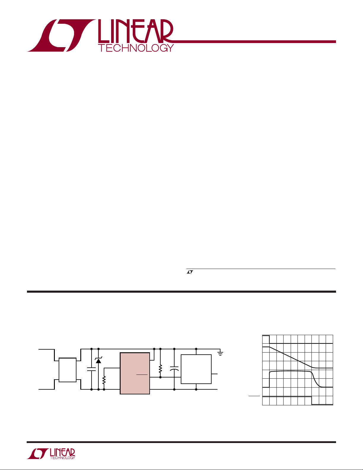
TYPICAL APPLICATIO
Powered Device (PD)
–48V FROM
POWER SOURCING
EQUIPMENT
(PSE)
~~+
DF01SA
0.1µF
–
SMAJ58A
R
CLASS
U
R
V
CLASS
IN
LTC4257
PWRGD
GND
V
OUT
100k
5µF
MIN
+
V
IN
SWITCHING
POWER SUPPLY
SHDN
RTN
4257 TA01
+
3.3V
TO LOGIC
–
V
50V/DIV
V
OUT
20V/DIV
200mA/DIV
PWRGD
50V/DIV
LTC4257 Charging 300µF
Load Capacitor
IN
I
IN
5ms/DIV
4225 TA02
4257fb
1
LTC4257
WWWU
ABSOLUTE AXI U RATI GS
(Notes 1, 2)
VIN Voltage ............................................. 0.3V to –100V
, PWRGD Voltage ............. VIN + 100V to VIN – 0.3V
V
OUT
R
PWRGD Current .................................................. 10mA
R
Voltage ............................ VIN + 7V to VIN – 0.3V
CLASS
Current .................................................. 100mA
CLASS
Operating Ambient Temperature Range
LTC4257C ............................................... 0°C to 70°C
LTC4257I............................................. –40°C to 85°C
Storage Temperature Range
S8 Package....................................... – 65°C to 150°C
DD Package ...................................... –65°C to 125°C
Lead Temperature (Soldering, 10 sec).................. 300°C
UU
W
PACKAGE/ORDER I FOR ATIO
TOP VIEW
TOP VIEW
1
NC
R
2
CLASS
NC
3
V
4
IN
S8 PACKAGE
8-LEAD PLASTIC SO
T
= 150°C, θJA = 150°C/W
JMAX
ORDER PART NUMBER S8 PART MARKING
LTC4257CS8
LTC4257IS8
Order Options Tape and Reel: Add #TR Lead Free: Add #PBF
Lead Free Tape and Reel: Add #TRPBF Lead Free Part Marking: http://www.linear.com/leadfree/
Consult LTC Marketing for parts specified with wider operating temperature ranges. *The temperature grades are identified by a label on the shipping container.
8
7
6
5
GND
NC
PWRGD
V
OUT
4257
4257I
ORDER PART NUMBER DD PART MARKING*
LTC4257IDD
1NC
R
2
CLASS
NC
3
V
4
IN
8-LEAD (3mm × 3mm) PLASTIC DFN
ELECTRICALLY ISOLATED PCB HEATSINK
DD PACKAGE
T
= 125°C, θJA = 43°C/W
JMAX
EXPOSED PAD TO BE SOLDERED TO
8
7
6
5
GND
NC
PWRGD
V
OUT
LACTLTC4257CDD
ELECTRICAL CHARACTERISTICS
temperature range, otherwise specifications are at T
SYMBOL PARAMETER CONDITIONS MIN TYP MAX UNITS
V
IN
I
IN_ON
I
IN_CLASS
∆I
CLASS
Supply Voltage Voltage with Respect to GND Pin (Notes 4, 5, 6)
Maximum Operating Voltage
Signature Range
Classification Range
UVLO Turn-On Voltage
UVLO Turn-Off Voltage
IC Supply Current when ON VIN = –48V, Pins 5, 6 Floating
IC Supply Current During Classification VIN = –17.5V, Pin 2 Floating, V
Current Accuracy During Classification 10mA < I
The ● denotes the specifications which apply over the full operating
= 25°C. (Note 3)
A
●
●
–1.5 –9.5 V
●
–12.5 – 21 V
●
–37.7 –39.2 –40.2 V
●
–29.3 –30.5 –31.5 V
●
(Note 7)
CLASS
(Notes 8, 9)
Tied to GND
OUT
< 40mA, –12.5V ≤ VIN ≤ – 21V,
●
0.35 0.50 0.65 mA
●
–57 V
3mA
±3.5 %
4257fb
2
LTC4257
ELECTRICAL CHARACTERISTICS
temperature range, otherwise specifications are at T
The ● denotes the specifications which apply over the full operating
= 25°C. (Note 3)
A
SYMBOL PARAMETER CONDITIONS MIN TYP MAX UNITS
R
SIGNATURE
Signature Resistance –1.5V ≤ VIN ≤ –9.5V, V
Tied to GND,
OUT
●
23.25 26.00 kΩ
IEEE 802.3af 2-Point Measurement (Notes 4, 5)
V
PG_OUT
V
PG_THRES_FALL
V
PG_THRES_RISE
I
PG_LEAK
R
ON
I
OUT_LEAK
I
LIMIT
I
LIMIT_WARM
T
OVERTEMP
T
SHUTDOWN
Note 1: Stresses beyond those listed under Absolute Maximum Ratings
may cause permanent damage to the device. Exposure to any Absolute
Maximum Rating condition for extended periods may affect device
reliability and lifetime.
Note 2: All voltages are with respect to GND pin.
Note 3: The LTC4257 operates with a negative supply voltage in the range
of –1.5V to –57V. To avoid confusion, voltages in this data sheet are
always referred to in terms of absolute magnitude. Terms such as
“maximum negative voltage” refer to the largest negative voltage and a
“rising negative voltage” refers to a voltage that is becoming more
negative.
Note 4: The LTC4257 is designed to work with two polarity protection
diodes between the PSE and PD. Parameter ranges specified in the
Electrical Characteristics are with respect to LTC4257 pins and are
designed to meet IEEE 802.3af specifications when these diode drops are
included. See Applications Information.
Note 5: Signature resistance is measured via the 2-point ∆V/∆I method as
defined by IEEE 802.3af. The LTC4257 signature resistance is offset from
25k to account for diode resistance. With two series diodes, the total PD
resistance will be between 23.75k and 26.25k and meet IEEE 802.3af
specifications. The minimum probe voltages measured at the LTC4257
pins are –1.5V and –2.5V. The maximum probe voltages are –8.5V and
–9.5V.
Note 6: The LTC4257 includes hysteresis in the UVLO voltages to preclude
Power Good Output Low Voltage I = 1mA, VIN = –48V, PWRGD Referenced to V
Power Good Trip Point VIN = –48V, Voltage Between VIN and V
V
Falling
OUT
V
Rising
OUT
Power Good Leakage VIN = 0V, PWRGD FET Off, V
PWRGD
OUT
= 57V
(Note 9)
On-Resistance I = 300mA, VIN = – 48V, Measured from VIN to V
(Note 9)
V
Leakage VIN = 0V, Power MOSFET Off, V
OUT
Input Current Limit VIN = –48V, V
= –43V (Note 11)
OUT
= 57V (Note 10)
OUT
●
IN
●
1.3 1.5 1.7 V
●
2.7 3.0 3.3 V
●
OUT
●
●
●
300 350 400 mA
1.0 1.6 Ω
0.5 V
1 µA
2.0 Ω
150 µA
Overtemperature Input Current Limit (Note 11) 188 mA
Overtemperature Trip Temperature (Note 11) 120 °C
Thermal Shutdown Trip Temperature (Note 11) 140 °C
power up from a voltage source with 20Ω series resistance on the first
trial.
Note 7: I
Pin 2. Total supply current in classification mode will be I
does not include classification current programmed at
IN_CLASS
IN_CLASS
+ I
CLASS
(see Note 8).
Note 8: I
∆I
CLASS
I
CLASS
include variations in R
a PD also includes the IC quiescent current (I
is the measured current flowing through R
CLASS
accuracy is with respect to the ideal current defined as
= 1.237/R
. The current accuracy specification does not
CLASS
resistance. The total classification current for
CLASS
IN_CLASS
). See Applications
CLASS
.
Information.
Note 9: For the DD package, this parameter is assured by design and
wafer level testing.
Note 10: I
OUT_LEAK
includes current drawn at the V
pin by the power
OUT
good status circuit. This current is compensated for in the 25kΩ signature
resistance and does not affect PD operation.
Note 11: The LTC4257 includes smart thermal protection. In the event of
an overtemperature condition, the LTC4257 will reduce the input current
limit by 50% to reduce the power dissipation in the package. If the part
continues heating and reaches the shutdown temperature, the current is
reduced to zero until the part cools below the overtemperature limit. The
LTC4257 is also protected against thermal damage from incorrect
classification probing by the PSE. If the LTC4257 exceeds the
overtemperature trip point, the classification load current is disabled.
any start-up oscillation. Per IEEE 802.3af requirements, the LTC4257 will
4257fb
3
LTC4257
UW
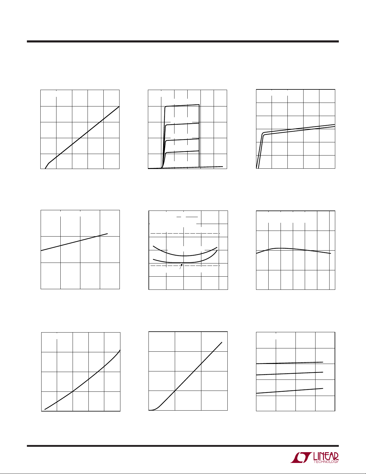
TYPICAL PERFOR A CE CHARACTERISTICS
Input Current vs Input Voltage
25k Detection Range Input Current vs Input Voltage
0.5
TA = 25°C
0.4
0.3
0.2
INPUT CURRENT (mA)
0.1
0
0
–4 –6 –8
–2
INPUT VOLTAGE (V)
–10
4357 G02
Input Current vs Input Voltage
50
TA = 25°C
40
30
20
INPUT CURRENT (mA)
10
0
0
CLASS 4
CLASS 3
CLASS 2
CLASS 1
CLASS 0
–20 –30 –40
–10
INPUT VOLTAGE (V)
–50 –60
4257 G01
12.0
CLASS 1 OPERATION
11.5
11.0
10.5
10.0
INPUT CURRENT (mA)
9.5
9.0
–12
85°C
–40°C
–14
–16
INPUT VOLTAGE (V)
–18
–20 –22
4257 G03
Input Current vs Input Voltage
3
EXCLUDES ANY LOAD CURRENT
= 25°C
T
A
2
1
INPUT CURRENT (mA)
0
–45 –55
INPUT VOLTAGE (V)
Power Good Output Low Voltage
vs Current
4
TA = 25°C
3
(V)
2
PG_OUT
V
1
4257 G04
Signature Resistance
vs Input Voltage
28
RESISTANCE =
27
DIODES: S1B
= 25°C
T
A
26
25
24
LTC4257 ONLY
SIGNATURE RESISTANCE (kΩ)
23
CURRENT (µA)
V
V1:
V2:
OUT
22
120
90
60
30
–1
–2 –4
V
OUT
= 0V
V
IN
= 25°C
T
A
–60–40 –50
∆V∆IV2 – V1
=
– I
I
2
1
IEEE UPPER LIMIT
LTC4257 + 2 DIODES
IEEE LOWER LIMIT
–3
–5
–6 –10
INPUT VOLTAGE (V)
Leakage Current
–9
–7
–8
4257 G05
Normalized UVLO Threshold
vs Temperature
2
APPLICABLE TO TURN-ON
AND TURN-0FF THRESHOLDS
1
0
–1
NORMALIZED UVLO THRESHOLD (%)
–2
–40
–20 0 20 40
TEMPERATURE (°C)
Current Limit vs Input Voltage
375
V
= VIN + 5V
OUT
365
355
345
CURRENT LIMIT (mA)
335
85°C
25°C
–40°C
60 80
4257 G06
4
0
2
0
CURRENT (mA)
6
8
4
10
4257 G07
0
0
20 40
V
PIN VOLTAGE (V)
OUT
60
42571 G09
325
–40
–45
–50
INPUT VOLTAGE (V)
–55
–60
4257 G09
4257fb
LTC4257
U
UU
PI FU CTIO S
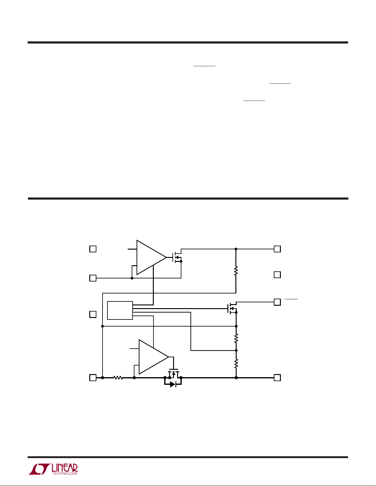
NC (Pin 1): No Connect.
R
(Pin 2): External Class Select Input. Used to set the
CLASS
current the LTC4257 maintains during classification. Connect a resistor between R
and VIN (see Table 2).
CLASS
NC (Pin 3): No Connect.
(Pin 4): Power Input. Tie to system –48V through the
V
IN
input diode bridge.
(Pin 5): Power Output. Supplies – 48V to the PD load
V
OUT
through an internal power MOSFET that limits input current. V
is high impedance until the input voltage rises
OUT
above the turn-on UVLO threshold. Above the UVLO
threshold the output is current limited to 350mA.
W
BLOCK DIAGRA
PWRGD (Pin 6): Power Good Output, Open-Drain. Signals
that the LTC4257 MOSFET is fully on. Low impedance
indicates power is good. PWRGD is high impedance
during detection, classification and in the event of a
thermal overload. PWRGD is referenced to V
IN
.
NC (Pin 7): No Connect
GND (Pin 8): Ground. Tie to system ground and to power
return through the input diode bridge.
R
NC
CLASS
NC
V
CLASSIFICATION
1
2
3
IN
1.237V
CONTROL
CIRCUITS
350mA
0.3Ω
CURRENT SOURCE
+
–
+
–
EN
EN
INPUT
CURRENT
LIMIT
25k SIGNATURE
RESISTOR
POWER GOOD
BOLD LINE INDICATES HIGH CURRENT PATH
8
7
6
54
GND
NC
PWRGD
V
OUT
4257 BD
4257fb
5
LTC4257
WUUU
APPLICATIO S I FOR ATIO
The LTC4257 is intended for use as the front end of a
Powered Device (PD) designed to IEEE 802.3af draft
standard. The LTC4257 includes a trimmed 25k signature
resistor, classification current source, and an inrush current limit circuit. With these functions integrated into the
LTC4257, the signature and power interface for a PD that
meets all the requirements of IEEE 802.3af can be built
with a minimum of external components.
Using an LTC4257 for the power and signature interface
functions of a PD provides several advantages. The
LTC4257 current limit circuit includes an onboard, 100V,
400mA power MOSFET with low leakage. This onboard
low leakage MOSFET avoids the possibility of corrupting
the 25k signature resistor while also saving board space
and cost. In addition, the IEEE 802.3af inrush current limit
requirement causes large transient power dissipation in
the PD; the LTC4257 manages this turn-on sequence
through the use of smart thermal protection circuitry. The
LTC4257 is designed to allow multiple turn-on sequences
without overheating the miniature 8-lead package. In the
event of excessive power cycling, the LTC4257 provides
thermally activated current-limit reduction to keep the
onboard power MOSFET within its safe operating area.
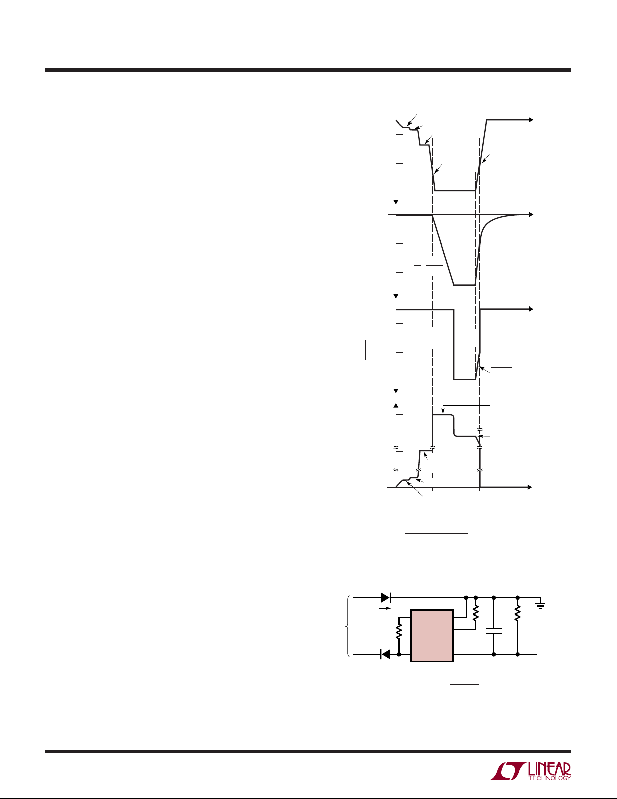
Operation
The LTC4257 has several modes of operation depending
on the applied input voltage as shown in Figure 1 and
summarized in Table 1. These various modes satisfy the
requirements defined in the IEEE 802.3af specification.
The input voltage is applied to the VIN pin and is with
reference to the GND pin. This input voltage is always
negative. To avoid confusion, voltages in this data sheet
are always referred to in terms of absolute magnitude.
Terms such as
largest negative voltage and a
maximum negative voltage
refer to the
rising negative voltage
refers to a voltage that is becoming more negative. References to electrical parameters in this applications section
use the nominal value. Refer to the Electrical Characteristics section for the range of values a particular parameter
will have.
PSE
–10
–20
(V)
IN
V
–30
–40
–50
–10
–20
(V)
OUT
–30
V
–40
–50
–10
–20
–30
PWRGD (V)
–40
–50
I
LIMIT
I
CLASS
PD CURRENT
V
IN
R
CLASS
UVLO
V1 – 2 DIODE DROPS
I
=
1
V2 – 2 DIODE DROPS
I2 =
I
CLASS
I
= 350mA (NOMINAL)
LIMIT
I
=
LOAD
2
I
IN
4
DETECTION V1
DETECTION V2
CLASSIFICATION
UVLO
TURN-ON
OFF
dV
=
dt
POWER
DEPENDENT ON R
V
R
LOAD
LTC4257
R
CLASS
V
IN
UVLO
I
LIMIT
C1
BAD
CLASSIFICATION
I
CLASS
DETECTION I
DETECTION I
25kΩ
25kΩ
IN
GND
PWRGD
V
OUT
ON
POWER
GOOD
2
1
CLASS
8
6
5
SELECTION
R9 R
TIME
UVLO
TURN-OFF
TIME
τ = R
LOAD
UVLO
OFF
TIME
POWER
BAD
PWRGD TRACKS
V
IN
CURRENT
LIMIT, I
LOAD CURRENT, I
LOAD
C1
Figure 1. Output Voltage, PWRGD and PD Current
as a Function of Input Voltage
LIMIT
C1
V
4257 F01
LOAD
GND
OUT
6
4257fb

WUUU
APPLICATIO S I FOR ATIO
LTC4257
Table 1. LTC4257 Operational Mode
as a Function of Input Voltage
INPUT VOLTAGE
with RESPECT to GND) LTC4257 MODE OF OPERATION
(V
IN
0V to –1.4V Inactive
–1.5V to – 10V 25k Signature Resistor Detection
–11V to – 12.4V Classification Load Current Ramps up from
0% to 100%
–12.5V to UVLO* Classification Load Current Active
UVLO* to –57V Power Applied to PD Load
*UVLO includes hysteresis.
Rising input threshold ≅ –39.2V
Falling input threshold ≅ –30.5V
Series Diodes
The IEEE 802.3af defined operating modes for a PD
reference the input voltage at the RJ45 connector on the
PD. However, PD circuitry must include diode bridges
between the RJ45 connector and the LTC4257 (Figure 2).
The LTC4257 takes this into account by compensating for
these diode drops in the threshold points for each range of
operation. Since the voltage ranges specified in the LTC4257
electrical specifications are with respect to the IC pins for
both the signature and classification ranges, the LTC4257
lower end extends two diode drops below the IEEE 802.3af
specification. A similar adjustment is made for the UVLO
voltages.
Detection
During detection, the PSE will apply a voltage in the range
of –2.8V to –10V on the cable and look for a 25k signature
resistor. This identifies the device at the end of the cable
as a PD. With the terminal voltage in this range, the LTC4257
connects an internal 25k resistor between GND and the V
IN
pins. This precision, temperature compensated resistor
presents the proper characteristics to alert the Power
Sourcing Equipment (PSE) at the other end of the cable that
a PD is present and desires power to be applied.
The power applied to a PD is allowed to use either of two
polarities and the PD must be able to accept this power so
it is common to install a diode bridge on the input. The
LTC4257 is designed to compensate for the voltage and
resistance effects of these two series diodes. The signature range extends below the IEEE range to accommodate
the voltage drop of the diodes. The IEEE specification
requires the PSE to use a ∆V/∆I measurement technique
to keep the DC offset of these diodes from affecting the
signature resistance measurement. However, the diode
resistance appears in series with the signature resistor
and must be included in the overall signature resistance
of the PD. The LTC4257 compensates for the two series
diodes in the signature path by offsetting the resistance
so that a PD built using the LTC4257 will meet the IEEE
requirements.
POWERED DEVICE (PD)
INTERFACE
AS DEFINED
BY IEEE 802.3af
Figure 2. PD Front End Using Diode Bridges on Main and Spare Inputs
RJ45
+
TX
1
–
TX
2
+
RX
3
–
RX
6
SPARE
4
5
7
SPARE
8
T1
TO PHY
+
BR2
–
BR1
8
GND
4
LTC4257
V
IN
4257 F02
4257fb
D3
7

LTC4257
WUUU
APPLICATIO S I FOR ATIO
Classification
Once the PSE has detected a PD, the PSE may optionally
classify the PD. Classification provides a method for more
efficient allocation of power by allowing the PSE to identify
lower-power PDs and allocate less power for these devices. IEEE 802.3af defines five classes (Table 2) with
varying power levels. The designer selects the appropriate
classification based on the power consumption of the PD.
For each class, there is an associated load current that the
PD asserts onto the line during classification probing. The
PSE measures the PD load current to determine the proper
classification and PD power requirements.
Table 2. Summary of IEEE 802.3af Power Classifications and
LTC4257 R
CLASS USAGE (W) (mA) (Ω, 1%)
0 Default 0.44 to 12.95 <5 Open
1 Optional 0.44 to 3.84 10.5 124
2 Optional 3.84 to 6.49 18.5 68.1
3 Optional 6.49 to 12.95 28 45.3
4 Reserved Reserved* 40 30.9
*Class 4 is currently reserved and should not be used.
Resistor Selection
CLASS
MAXIMUM NOMINAL LTC4257
POWER LEVELS CLASSIFICATION R
AT INPUT OF PD LOAD CURRENT RESISTOR
CLASS
Early revisions of the IEEE 802.3af draft specification
defined two methods that a PSE could use in order to
perform PD classification. These methods are known as
Measured Current and Measured Voltage. The IEEE has
since removed the Measured Voltage method from the
specification. The LTC4257 is compatible with the IEEE
802.3af standard and also works with the obsolete Measured Voltage method.
In the Measured Current method (Figure 3), the PSE
presents a fixed voltage between –15.5V and –20V to the
PD. With the input voltage in this range, the LTC4257
asserts a load current from the GND pin through the
R
with the selection of the R
resistor. The magnitude of the load current is set
CLASS
resistor. The resistor value
CLASS
associated with each class is shown in Table 2.
In the Measured Voltage method (Figure 4), the PSE drives
a current into the PD and monitors the voltage across the
PD terminals. The PSE current steps between classification load current values in order to classify the PD under
test. For PSE probe currents below the PD load current, the
LTC4257 will keep the PD terminal voltage below the
classification voltage range. For PSE probe currents above
the PD load current, the LTC4257 will force the PD terminal
voltage above the classification voltage range.
During classification, a moderate amount of power is
dissipated in the LTC4257. IEEE 802.3af limits the classification time to 75ms. The LTC4257 is designed to handle
the power dissipation for this time period. If the PSE
CURRENT PATH
PSE
PROBING
VOLTAGE
SOURCE
–15.5V TO –20.5V
R
V
PSE CURRENT MONITOR
PSE
CLASS
4
LTC4257
R
CLASS
V
IN
PD
Figure 3. IEEE 802.3af Measured-Current Method
of Classification Probing
8
GND
4257 F03
82
CONSTANT
LOAD
CURRENT
INTERNAL
TO LTC4257
CURRENT PATH
PSE
PROBING
CURRENT
SOURCE
IF PSE PROBING CURRENT < LTC4257 LOAD CURRENT, PD TERMINAL VOLTAGE IS < 15V
IF PSE PROBING CURRENT > LTC4257 LOAD CURRENT, PD TERMINAL VOLTAGE IS > 20V
V
PSE
VOLTAGE
MONITOR
R
CLASS
4
PDPSE
LTC4257
R
CLASS
V
IN
GND
82
CONSTANT
LOAD
CURRENT
INTERNAL
TO LTC4257
4257 F04
Figure 4. IEEE 802.af Measured-Voltage Method
of Classification Probing
4257fb

WUUU
APPLICATIO S I FOR ATIO
LTC4257
probing exceeds 75ms, the LTC4257 may overheat. In this
situation, the thermal protection circuit will engage and
disable the classification current source in order to protect
the part. The LTC4257 stays in classification mode until
the input voltage rises above the UVLO turn-on voltage.
Undervoltage Lockout
I
EEE 802.3af dictates a maximum turn-on voltage of 42V
and a minimum turn-off voltage of 30V for the PD. In
addition, the PD must maintain large on-off hysteresis to
prevent resistive losses in the wiring between the PSE and
the PD from causing start-up oscillation. The LTC4257
incorporates an undervoltage lockout (UVLO) circuit that
monitors line voltage to determine when to apply power
to the PD load (Figure 5). Before power is applied to the
load, the V
pin is high impedance and at ground
OUT
potential since there is no charge on capacitor C1. When
the input voltage rises above the UVLO turn-on threshold,
the LTC4257 removes the classification load current and
turns on the internal power MOSFET. C1 charges up under
LTC4257 current limit control and the V
pin transitions
OUT
from 0V to V
. This sequence is shown in Figure 1. The
IN
LTC4257 includes a hysteretic UVLO circuit that keeps
power applied to the load until the input voltage falls
below the UVLO turn-off threshold. Once the input voltage
drops below –30V, the internal power MOSFET is turned
off and the classification load current is re-enabled.
C1 will discharge through the PD circuitry and the V
OUT
pin will go to a high impedance state.
Input Current Limit
IEEE 802.3af specifies a maximum inrush current and also
specifies a minimum load capacitor between the GND and
V
pins. To control turn-on surge current in the system,
OUT
the LTC4257 integrates a current limit circuit with the
onboard power MOSFET and sense resistor to provide a
complete inrush control circuit without additional external
components. The LTC4257 limits input current to less
than the 400mA maximum specified by 802.3af, allowing
the load capacitor to ramp up to the line voltage in a
controlled manner. During this ramp up, a large amount of
power is dissipated in the power MOSFET. The LTC4257
PSE
+
LTC4257
TO
4
UNDERVOLTAGE
LOCKOUT
CIRCUIT
V
IN
INPUT LTC4257
VOLTAGE POWER MOSFET
0V TO UVLO* OFF
>UVLO* ON
*UVLO INCLUDES HYSTERESIS
RISING INPUT THRESHOLD ≅ –39.2V
FALLING INPUT THRESHOLD ≅ –30.5V
Figure 5. LTC4257 Undervoltage Lockout
GND
V
OUT
8
5
C1
5µF
MIN
4257 F05
CURRENT-LIMITED
TURN ON
PD
LOAD
4257fb
9

LTC4257
WUUU
APPLICATIO S I FOR ATIO
is designed to accept this thermal load and is thermally
protected to avoid damage to the onboard power MOSFET.
Note that the PD designer must ensure that the PD steadystate power consumption falls within the limits shown in
Table 2.
Power Good
The LTC4257 includes a power good circuit (Figure 6) that
is used to indicate to the PD circuitry that load capacitor C1
is fully charged and that the PD can start DC/DC converter
operation. The power good circuit monitors the voltage
across the internal power MOSFET and PWRGD is asserted when the voltage drops below 1.5V. The power
good circuit includes a large amount of hysteresis to allow
the LTC4257 to operate near the current limit point without
inadvertently disabling PWRGD. The MOSFET voltage
must increase to 3V before PWRGD is disabled.
If a sudden increase in voltage appears on the input line,
this voltage step will be transferred through capacitor C1
and appear across the power MOSFET. The response of
the LTC4257 will depend on the magnitude of the voltage
step, the rise time of the step, the value of capacitor C1 and
the DC load. For fast rising inputs, the LTC4257 will
attempt to quickly charge capacitor C1 using an internal
secondary current limit circuit. In this scenario, the PSE
current limit should provide the overall limit for the circuit.
For slower rising inputs, the 350mA current limit in the
LTC4257 will set the charge rate of capacitor C1. In either
case, the PWRGD signal may go inactive briefly while the
capacitor is charged up to the new line voltage. In the
design of a PD, it is necessary to determine if a step in the
input voltage will cause the PWRGD signal to go inactive
and how to respond to this event. In some designs, the
charge on C1 is sufficient to power the PD through this
event. In this case, it may be desirable to filter the PWRGD
signal so that intermittent power bad conditions are
ignored. Figure 10 demonstrates methods to insert a
lowpass filter on the power good interface.
For PD designs that use a large load capacitor and also
consume a lot of power, it is important to delay activation
of the PD circuitry with the PWRGD signal. If the PD circuitry is not disabled during the current-limited turn-on sequence, the PD circuitry will rob current intended for charging up the load capacitor and create a slow rising input,
possibly causing the LTC4257 to go into thermal shutdown.
The PWRGD pin connects to an internal open-drain, 100V
transistor capable of sinking 1mA. Low impedance indicates power is good. PWRGD is high impedance during
signature and classification probing and in the event of a
thermal overload.
During turn-off, PWRGD is deactivated when the input
voltage drops below 30V. In addition, PWRGD may go
active briefly at turn-on for fast rising input waveforms.
PWRGD is referenced to the V
be near the V
potential. The PD DC/DC converter will
IN
typically be referenced to V
pin and when active will
IN
and care must be taken to
OUT
ensure that the difference in potential of the PWRGD signal
does not cause any detrimental effects. Use of diode clamp
D6, as shown in Figure 10, will alleviate any problems.
10
PSE
OUT
R9
100k
6
5µF
MIN
5
SHDN
PD
LOAD
+
C1
4257 F06
4257fb
LTC4257
THERMAL SHUTDOWN
UVLO
TO
V
4
IN
Figure 6. LTC4257 Power Good
–
+
+
–
1.125V
300k
PWRGD
300k
V

WUUU
APPLICATIO S I FOR ATIO
LTC4257
Thermal Protection
The LTC4257 includes smart thermal protection in order
to provide full device functionality in a miniature package
while maintaining safe operating temperatures. Several
factors create the possibility for tremendous power
dissi
pation within the LTC4257. IEEE 802.3af mandates
that inrush current be limited to less than 400mA while
standard telecom power can be as high as 57V. At turn on,
before the load capacitor has charged up, the instantaneous power dissipated by the LTC4257 can be over 20W.
As the load capacitor charges up, the power dissipation in
the LTC4257 will decrease until it reaches a steady-state
value dependent on the DC load current. The size of the
load capacitor determines how fast the power dissipation
in the LTC4257 subsides. At room temperature, the
LTC4257 can handle load capacitors as large as 800µF
without going into thermal shutdown. With a large load
capacitor like this, the LTC4257 die temperature will
increase by about 50°C during a single turn-on sequence.
If for some reason power were removed from the part and
then quickly reapplied so that the LTC4257 had to charge
up the load capacitor again, the temperature rise would be
excessive if safety precautions were not implemented.
The LTC4257 protects itself from thermal damage by
monitoring the die temperature. If the die temperature
exceeds the overtemperature trip point, the part switches
to a half-power mode where the current limit is set to 50%
of its normal level. This reduces power dissipation and
helps prevent further heating. If the part continues to heat
up and reaches the shutdown temperature, the current is
reduced to zero and very little power is dissipated in the
T > 120°C
UVLO
TURN ON
100%
CURRENT
part until it cools below the overtemperature set point. The
LTC4257 current limit will continue switching between
0%, 50% and 100% current levels (Figure 7) until the load
capacitor is fully charged.
If the PD is designed to operate at a high ambient temperature and with the maximum allowable supply (57V), there
will be a limit to the size load capacitor that can be charged
up before the LTC4257 reaches the overtemperature trip
point. Hitting the overtemperature trip point intermittently
does not harm the LTC4257, but it will delay completion of
capacitor charging. Capacitors up to 200µF can be charged
without a problem.
During classification, excessive heating of the LTC4257
can occur if the PSE violates the 75ms probing time limit.
To protect the LTC4257, the thermal protection circuitry
will disable classification current if the die temperature
exceeds the overtemperature trip point. When the die
cools down below the trip point, classification current is
re-enabled.
Once the LTC4257 has charged up to the load capacitor
and the PD is powered and running, there will be some
residual heating due to the DC load current of the PD
flowing through the internal MOSFET. In some applications, the LTC4257 power dissipation may be significant
and if dissipated in the S8 package, excessive package
heating could occur. This problem can be solved with the
use of the DD package which has superior thermal performance. The DD package includes an exposed pad that
should be soldered to an isolated heatsink on the printed
circuit board.
50%
CURRENT
T < 120°C
T < 120°C
0%
CURRENT
Figure 7. Smart Thermal Protection State Diagram
T > 140°C
4257 F07
4257fb
11

LTC4257
WUUU
APPLICATIO S I FOR ATIO
EXTERNAL INTERFACE AND COMPONENT SELECTION
Transformer
Nodes on an Ethernet network commonly interface to the
outside world via an isolation transformer (Figure 8). For
powered devices, the isolation transformer must include
a center tap on the media (cable) side. Proper termination
is required around the transformer to provide correct
impedance matching and to avoid radiated and conducted
emissions. Transformer vendors such as Pulse, Bel Fuse,
Tyco and others (Table 3) can provide assistance with
selection of an appropriate isolation transformer and
proper termination methods. These vendors have transformers specifically designed for use in PD applications.
Table 3. Power over Ethernet Transformer Vendors
VENDOR CONTACT INFORMATION
Pulse Engineering 12220 World Trade Drive
San Diego, CA 92128
Tel: 858-674-8100
FAX: 858-674-8262
http://www.pulseeng.com/
Bel Fuse Inc. 206 Van Vorst Street
Jersey City, NJ 07302
Tel: 201-432-0463
FAX: 201-432-9542
http://www.belfuse.com/
Tyco Electronics 308 Constitution Drive
Menlo Park, CA 94025-1164
Tel: 800-227-7040
FAX: 650-361-2508
http://www.circuitprotection.com/
Diode Bridges
IEEE 802.3af allows power wiring in either of two configurations on the TX/RX wires, plus power can be applied to
the PD via the spare wire pair in the RJ45 connector. The
PD is required to accept power in either polarity on both
the main and spare inputs, therefore it is common to install
diode bridges on both inputs in order to accommodate the
different wiring configurations. Figure 8 demonstrates an
implementation of these diode bridges. The specification
also mandates that the leakage back through the unused
bridge be less than 28µA when the PD is powered with
57V.
The IEEE standard includes an AC impedance requirement
in order to implement the AC disconnect function. Capacitor C14 in Figure 8 is used to meet this AC impedance
requirement. A 0.1µF capacitor is recommended for this
application.
The LTC4257 has several different modes of operation
based on the voltage present between the V
and GND
IN
pins. The forward voltage drop of the input diodes in a PD
design subtracts from the input voltage and will affect the
transition point between modes. When using the LTC4257,
it is necessary to pay close attention to this forward
voltage drop. Selection of oversized diodes will help keep
the PD thresholds from exceeding IEEE specifications.
The input diode bridge of a PD can consume 4% of the
avialable power in some applications. It may be desirable
to use Scottky diodes in order to reduce this power loss.
12
RJ45
+
TX
1
–
TX
2
+
RX
3
–
RX
6
+
SPARE
4
5
7
8
SPARE
–
1
T1
16
2
15
3
14
6
11
7
10
8
9
PULSE H2019
TO PHY
BR2
DF01SA
C14
0.1µF
100V
BR1
DF01SA
SMAJ58A
TVS
8
GND
54
4257 F08
C1
V
OUT
D3
LTC4257
V
INVOUT
Figure 8. PD Front End with Isolation Transformer, Diode Bridges and Capacitor
4257fb

WUUU
APPLICATIO S I FOR ATIO
LTC4257
However, if the standard diode bridge is replaced with a
Schottky bridge, the transition points between modes will
be affected. The application circuit (Figure 11) shows a
technique for using Schottky diodes while maintaining
proper threshold points to meet IEEE 802.3af compliance.
Auxiliary Power Source
In some applications, it may be desirable to power the PD
from an auxiliary power source such as a wall transformer.
The auxiliary power can be injected into the PD at several
locations and various trade-offs exist. Power can be
injected at the 3.3V or 5V output of the isolated power
supply with the use of a diode ORing circuit. This method
accesses the internal circuits of the PD after the isolation
barrier and therefore meets the 802.3af isolation safety
requirements for the wall transformer jack on the PD.
Power can also be injected into the PD interface portion of
the LT4257. In this case, it is necessary to ensure the user
cannot access the terminals of the wall transformer jack
on the PD since this would compromise the 802.3af
isolation safety requirements. Figure 9 demonstrates three
methods of diode ORing external power into a PD. Option
1 inserts power before the LTC4257 while options 2 and 3
insert power after the LTC4257.
If power is inserted before the LTC4257 (option 1), it is
necessary for the wall transformer to exceed the LTC4257
UVLO turn-on requirement and limit the maximum voltage
to 57V. This option provides input current limiting for the
transformer, provides valid power good signaling and simplifies power priority issues. As long as the wall transformer
applies power to the PD before the PSE, it will take priority
and the PSE will not power up the PD because the wall power
will corrupt the 25k signature. If the PSE is already powering the PD, the wall transformer power will be in parallel
with the PSE. In this case, priority will be given to the higher
supply voltage. If the wall transformer voltage is higher, the
PSE should remove line voltage since no current will be
drawn from the PSE. On the other hand, if the wall transformer voltage is lower, the PSE will continue to supply
power to the PD and the wall transformer power will not be
used. Proper operation should occur in either scenario.
Auxiliary power can be applied after the LTC4257 as shown
in option 2. In this configuration, the wall transformer does
not need to exceed the LTC4257 turn-on UVLO requirement;
however, it is necessary to include diode D9 to prevent the
transformer from applying power to the LTC4257. The
transformer voltage requirements will be governed by the
needs of the PD switcher and may exceed 57V. However,
power priority issues require more intervention. If the wall
transformer voltage is below the PSE voltage, then priority
will be given to the PSE power. The PD will draw power from
the PSE while the transformer will sit unused. This configuration is not a problem in a PoE system. On the other hand,
if the wall transformer voltage is higher than the PSE voltage, the PD will draw power from the transformer. In this
situation, it is necessary to address the issue of power
cycling that may occur if a PSE is present. The PSE will detect
the PD and apply power. If the PD is being powered by the
wall transformer, then the PD will not meet the minimum
load requirement and the PSE will subsequently remove
power. The PSE will again detect the PD and power cycling
will start. With a transformer voltage above the PSE voltage, it is necessary to install a minimum load on the output
of the LTC4257 to prevent power cycling. Refer to the
LTC4257-1 data sheet for an alternative implementation of
option 2 which uses the Signature Disable feature.
The third option also applies power after the LTC4257, while
omitting diode D9. With the diode omitted, the transformer
voltage is applied to the LTC4257 in addition to the load.
For this reason, it is necessary to ensure that the transformer
maintain the voltage between 44V and 57V to keep the
LTC4257 in its normal operating range. The third option has
the advantage of automatically disabling the 25k signature
when the external voltage exceeds the PSE voltage.
4257fb
13

LTC4257
WUUU
APPLICATIO S I FOR ATIO
OPTION 1: AUXILIARY POWER INSERTED BEFORE LTC4257
RJ45
1
2
3
6
4
5
7
8
RJ45
1
2
3
6
4
5
7
8
TX
TX
RX
RX
TX
TX
RX
RX
+
–
+
–
SPARE
SPARE
+
–
+
–
SPARE
SPARE
+
–
ISOLATED
WALL
TRANSFORMER
+
–
ISOLATED
WALL
TRANSFORMER
T1
TO PHY
+
44V TO 57V
–
OPTION 2: AUXILIARY POWER INSERTED AFTER LTC4257
T1
TO PHY
+
–
~~+
BR1
DF01SA
~~+
BR2
DF01SA
~~+
BR1
DF01SA
~~+
BR2
DF01SA
D3
SMAJ58A
TVS
–
–
45
D8
S1B
D3
SMAJ58A
TVS
–
–
45
LTC4257
V
INVOUT
LTC4257
V
INVOUT
C14
0.1µF
100V
GND
C14
0.1µF
100V
GND
PD
C1
8
MINIMUM
LOAD
8
S1B
D10
S1B
LOAD
PD
C1
LOAD
D9
14
RJ45
1
2
3
6
4
5
7
8
TX
TX
RX
RX
+
–
+
–
SPARE
SPARE
OPTION 3: AUXILIARY POWER APPLIED TO LTC4257 AND PD LOAD
T1
~~+
TO PHY
BR1
DF01SA
–
+
~~+
BR2
–
DF01SA
–
ISOLATED
WALL
TRANSFORMER
+
44V TO 57V
–
Figure 9. Auxiliary Power Source for PD
D3
SMAJ58A
TVS
45
LTC4257
V
INVOUT
C14
0.1µF
100V
GND
D10
S1B
8
C1
42571 F09
PD
LOAD
4257fb

WUUU
APPLICATIO S I FOR ATIO
LTC4257
Classification Resistor Selection (R
CLASS
)
IEEE 802.3af allows classifying PDs into four distinct
classes with class 4 being reserved for future use (Table 2).
An external resistor connected from R
CLASS
to VIN (Figure 3) sets the value of the classification current. The
designer should determine which power category the PD
falls into and then select the appropriate value of R
CLASS
from Table 2. If a unique classification current is required,
the value of R
CLASS
IN_CLASS
= 1.237V/(I
R
where I
can be calculated as:
CLASS
DESIRED
– I
IN_CLASS
)
is the LTC4257 IC supply current during
classification and is given in the electrical specifications.
The R
resistor must be 1% or better to avoid
CLASS
degrading the overall accuracy of the classification circuit. Resistor power dissipation will be 50mW maximum
and is transient so heating is typically not a concern. In
order to maintain loop stability, the layout should
minimize capacitance at the R
tion circuit can be disabled by floating the R
node. The classifica-
CLASS
CLASS
pin. The
R
pin should not be shorted to VIN as this would
CLASS
force the LTC4257 classification circuit to attempt to
source very large currents. In this case, the LTC4257 will
quickly go into thermal shutdown.
Power Good Interface
The PWRGD signal is controlled by a high voltage, opendrain transistor. Examples of active-high and active-low
interface circuits for controlling the PD load are shown in
Figure 10.
In some applications it is desirable to ignore intermittent
power bad conditions. This can be accomplished by
including capacitor C15 in Figure 10 to form a lowpass
filter. With the components shown, power bad conditions
less than about 200µs will be ignored. Conversely, in other
applications it may be desirable to delay assertion of
PWRGD to the PD load. The PWRGD signal can be delayed
with the addition of capacitor C17 in Figure 10.
TO
PSE
TO
PSE
–48V
–48V
ACTIVE-LOW ENABLE, 5.1V SWING
8
GND
LTC4257
6
PWRGD
V
4
IN
LTC4257
PWRGD
V
4
IN
+
V
5
OUT
*C15 OPTIONAL TO FILTER PWRGD.
SEE APPLICATIONS INFORMATION
ACTIVE-HIGH ENABLE FOR RUN PIN WITH INTERNAL PULLUP
8
GND
6
+
V
5
OUT
*C15 AND C17 OPTIONAL TO FILTER PWRGD.
SEE APPLICATIONS INFORMATION
C1
5µF
100V
C1
5µF
100V
R9
100k
R18
10k
R9
100k
R18
10k
D6
5.1V
MMBZ5231B
D6
MMBD4148
C15*
0.047µF
10V
INTERNAL
PULLUP
FMMT2222
C15*
0.047µF
10V
Q1
PD
LOAD
SHDN
RUN
C17*
PD
LOAD
4257 F10
Figure 10. Power Good Interface Examples
4257fb
15

LTC4257
WUUU
APPLICATIO S I FOR ATIO
Load Capacitor
IEEE 802.3af requires that the PD maintain a minimum
load capacitance of 5µF. It is permissible to have a much
larger load capacitor and the LTC4257 can charge very
large load capacitors before thermal issues become a
problem. However, the load capacitor must not be too
large or the PD design may violate two IEEE 802.3af
requirements. The LTC4257 goes into current limit at
turn-on and charges the load capacitor with between
300mA and 400mA. The IEEE specification allows this
level of inrush current for up to 50ms. Therefore, it is
necessary that the PD complete charging of the capacitor
within the 50ms time limit. With a maximum input voltage
of –57V, these conditions limit the size of the load
capacitor to 250µF.
Very small output capacitors (≤ 10µF) will charge very
quickly in current limit. The rapidly changing voltage at
the output may reduce the current limit temporarily,
causing the capacitor to charge at a somewhat reduced
rate. Conversely, charging very large capacitors may
cause the current limit to increase slightly. In either case,
once the output voltage reaches its final value, the input
current limit will be restored to its nominal value.
If the load capacitor is too large there can be an additional
problem with inadvertent power shutdown by the PSE.
Consider the following scenario. If the PSE is running at
– 57V (maximum allowed) and the PD has been detected
and powered up, the load capacitor will be charged to
nearly – 57V. If for some reason the PSE voltage suddenly
is reduced to – 44V (minimum allowed), the input diodes
will reverse bias and PD power will be supplied solely by
the load capacitor. Depending on the size of the load
capacitor and the DC load of the PD, the PD will not draw
any power from the PSE for a period of time. If this period
of time exceeds the IEEE 802.3af 300ms disconnect
delay, the PSE may remove power from the PD. For this
reason, it is necessary to evaluate the load capacitance
and load current to ensure that inadvertent shutdown
cannot occur.
Maintain Power Signature
In an IEEE 802.3af system, the PSE uses the
power signature
require power. The MPS requires the PD to periodically
draw at least 10mA and also have an AC impedance less
than 26.25kΩ in parallel with 0.05µF. The PD application
circuits shown in this data sheet meet the requirements
necessary to maintain power. If either the DC current is
less than 10mA or the AC impedance is above 26.25kΩ,
the PSE might disconnect power. The DC current must be
less than 5mA and the AC impedance must be above 2MΩ
to guarantee power will be removed.
(MPS) to determine if a PD continues to
maintain
16
4257fb

WUUU
APPLICATIO S I FOR ATIO
LTC4257
Layout
The LTC4257 is relativity immune to layout problems.
Excessive parasitic capacitance on the R
be avoided. If using the DD package, include an electrically
isolated heat sink to which the exposed pad on the bottom
of the package can be soldered. For optimal thermal
performance, make the heat sink as large as possible.
Voltages in a PD can be as large as –57V, so high voltage
layout techniques should be employed.
The load capacitor connected between Pins 5 and 8 of the
LTC4257 can store significant energy when fully charged.
The design of a PD must ensure that this energy is not
inadvertently dissipated in the LTC4257. The polarityprotection diode(s) prevent an accidental short on the
CLASS
pin should
cable from causing damage. However, if the VIN pin is
shorted to the GND pin inside the PD while the load
capacitor is charged, current will flow through the parasitic body diode of the internal MOSFET and may cause
permanent damage to the LTC4257.
Input Surge Suppression
The LTC4257 is specified to operate with an absolute
maximum voltage of –100V and is designed to tolerate
brief overvoltage events. However, the pins that interface
to the outside world (primarily VIN and GND) can routinely
see peak voltages in excess of 10kV. To protect the
LTC4257, it is highly recommended that a transient voltage suppressor be installed between the bridge and the
LTC4257 (D3 in Figure 2).
4257fb
17

LTC4257
•
1
•
•
5
4
•
1
3
2
RX
–
SPARE
–
6
RX
+
3
TX
–
2
TX
+
J2
IN
FROM
PSE
T1
RJ45
1
7
8
5
4
6
8
7
TXOUT
+
OUT
TO PHY
TXOUT
–
SPARE
+
RXOUT
+
RXOUT
–
16
14
15
11
9
10
C19
47pF
C13
470pF
V
OUT
+
V
OUT
–
R24
100k
R28
10k
R23
3.65k
1%
R13
30.1k
1%
R17
10k
R14
100k
R11
10k
R10
62k
R25
62k
R26
10k
R27
62k
C20
0.47µF
C21
0.1µF
NOTES: UNLESS OTHERWISE SPECIFIED
1. ALL RESISTORS ARE 5%
2. ALL CAPACITORS ARE 25V
3. SELECT R
CLASS
FOR CLASS 1-4 OPERATION. REFER
TO DATA SHEET APPLICATIONS INFORMATION SECTION
4. CONNECT TO CHASSIS GROUND
C4 TO C6: TDK C4532X5R0J107M
C2, C23: AVX 1808GC102MAT
D1, D7: MM3Z12VT1
D3: MMBD1505
D9 TO D12, D14 TO D16: DIODES INC., B1100
L1: COILCRAFT D01608C-472
T1: PULSE H2019
T2: PULSE PB2134
T3: PULSE PA0184
OSCAP SFSTt
ON
ENDLYMINENAB
LT1737CGN
R
OCMP
V
CC
R
CMPC
UVLO GATE
SGND PGND
V
C
FB
3V
OUT
I
SENSE
C22
680pF
0603
D8
BAT54
D5
B0540W
C17
3300pF
R15
0.22Ω
1/2W
1%
R4
10k
T2
SEPARATING
LINE
FOR GROUND
PLANE
T3
8
D7
12V
1
C12
0.1µF
50V
C10
4.7µF
35V
R16
330Ω
C16
0.1µF
50V
C23
1000pF
2kV
•
9
10
3
•
5
4
C18
1nF
R18
100Ω
Q6
Si7892DP
Q7
FMMT718
Q8
MMBT3904
8
11
C14
1µF
R12
47Ω
C4 TO C6
100µF
6.3V
3.3V @ 2.8A
Q3
Si4490DY
LTC4257CDD
R
CLASS
1%
NC
R
CLASS
NC
V
IN
GND
NC
PWRGD
V
OUT
C1B
0.82µF
100V
C1C
0.82µF
100V
L1
4.7µH
Q2
MMBT3904
Q4
MMBT2907ALT1
Q5
MMBT3904
R9
100Ω
R8
47Ω
R6
47Ω
C9
100pF
D2
BAT54
Q1
MMBTA06
D4
BAS21LT1
D1
12V
D3A D3B
R7
33Ω
1/4W
C1A
10µF
100V
R5
47K
+
Q9
2N7002
D13
MMSD4148
C11
0.1µF
100V
D6
SMAJ58A
R30
75Ω
C24
0.01µF
200V
R31
75Ω
C25
0.01µF
200V
R1
75Ω
C7
0.01µF
200V
R2
75Ω
C3
0.01µF
200V
C2
1000pF
2kV
4257 TA04
D10
B1100
D12
B1100
D9
B1100
D11
B1100
D17
B1100
D16
B1100
D15
B1100
D14
B1100
3
4
4
TYPICAL APPLICATIO
U
Figure 11: PD Power Interface with 3.3V, 2.8A High Efficiency Isolated Power Supply
18
4257fb

PACKAGE DESCRIPTIO
.045 ±.005
.160
±.005
.245
MIN
.050 BSC
U
S8 Package
8-Lead Plastic Small Outline (Narrow .150 Inch)
(Reference LTC DWG # 05-08-1610)
.189 – .197
(4.801 – 5.004)
NOTE 3
.228 – .244
(5.791 – 6.197)
7
8
5
6
.150 – .157
(3.810 – 3.988)
NOTE 3
.053 – .069
(1.346 – 1.752)
.014 – .019
(0.355 – 0.483)
TYP
LTC4257
.004 – .010
(0.101 – 0.254)
.050
(1.270)
BSC
.030 ±.005
TYP
RECOMMENDED SOLDER PAD LAYOUT
NOTE:
1. DIMENSIONS IN
2. DRAWING NOT TO SCALE
3.5 ±0.05
INCHES
(MILLIMETERS)
1.65 ±0.05
(2 SIDES)2.15 ±0.05
0.25 ± 0.05
RECOMMENDED SOLDER PAD PITCH AND DIMENSIONS
1
3. THESE DIMENSIONS DO NOT INCLUDE MOLD FLASH OR PROTRUSIONS.
MOLD FLASH OR PROTRUSIONS SHALL NOT EXCEED .006" (0.15mm)
3
2
4
DD Package
8-Lead Plastic DFN (3mm × 3mm)
(Reference LTC DWG # 05-08-1698)
0.675 ±0.05
PIN 1
TOP MARK
(NOTE 6)
0.200 REF
NOTE:
1. DRAWING TO BE MADE A JEDEC PACKAGE OUTLINE M0-229 VARIATION OF (WEED-1)
2. DRAWING NOT TO SCALE
3. ALL DIMENSIONS ARE IN MILLIMETERS
4. DIMENSIONS OF EXPOSED PAD ON BOTTOM OF PACKAGE DO NOT INCLUDE
MOLD FLASH. MOLD FLASH, IF PRESENT, SHALL NOT EXCEED 0.15mm ON ANY SIDE
5. EXPOSED PAD SHALL BE SOLDER PLATED
6. SHADED AREA IS ONLY A REFERENCE FOR PIN 1 LOCATION
ON TOP AND BOTTOM OF PACKAGE
2.38 ±0.05
(2 SIDES)
0.50
BSC
PACKAGE
OUTLINE
.008 – .010
(0.203 – 0.254)
3.00 ±0.10
(4 SIDES)
0.75 ±0.05
1.65 ± 0.10
0.00 – 0.05
.010 – .020
(0.254 – 0.508)
(2 SIDES)
× 45°
.016 – .050
(0.406 – 1.270)
R = 0.115
TYP
0.25 ± 0.05
BOTTOM VIEW—EXPOSED PAD
2.38 ±0.10
(2 SIDES)
0°– 8° TYP
0.38 ± 0.10
85
14
0.50 BSC
SO8 0303
(DD8) DFN 1203
Information furnished by Linear Technology Corporation is believed to be accurate and reliable.
However, no responsibility is assumed for its use. Linear Technology Corporation makes no representation that the interconnection of its circuits as described herein will not infringe on existing patent rights.
4257fb
19

LTC4257
TYPICAL APPLICATIO
RJ45
J1
+
TX
1
TX
2
RX
3
RX
6
4
5
7
8
1
T1
16
TXOUT
2
15
–
3
14
+
–
SPARE
SPARE
TXOUT
6
11
RXOUT
7
10
8
9
RXOUT
XFMR
+
75Ω
–
NOTES: UNLESS OTHERWISE SPECIFIED
1. ALL RESISTOR VALUES ARE 5%
2. SELECT R
REFER TO DATA SHEET APPLICATIONS INFORMATION SECTION
3. CONNECT TO CHASSIS GROUND
C1A: PANASONIC ECEV2AA4R7P
C1B: TDK C5750X7R2A225KT
C8: AVX 1808GC102MAT
C9, C10, C12, C13: TDK C4532X5ROJ107
L1: LQLB2518T1ROM
T1: PULSE H2019
R12
75Ω
+
C4
0.01µF
–
200V
TO
+
PHY
C3
0.01µF
200V
–
R11
75Ω
0.01µF
0.01µF
200V
75Ω
200V
FOR CLASS 1-4 OPERATION.
CLASS
3
C8
0.001µF
2kV
U
PD Power Interface with 3.3V, 3A Nonisolated Power Supply
L1
1µH
+
~+
BR1
DF01SA
~–
~+
BR2
DF01SA
~–
D3
TVS
SMAJ58A
C14
0.1µF
100V
1N4148
R9
100k
R18
10k
C1A
4.7µF
100V
LTC4257
NC
GND
R
NC
V
R
CLASS
1%
2
D6
FMMT2222
R16
100Ω
CLASS
IN
Q4
R17
750Ω
R10
100k
PWRGD
V
1µF 6.3V
NC
OUT
Q1
2N7002
80.6k
C
1nF
C6
R
1%
C1
C1B
2.2µF
100V
MMBZ5235B
LTC1871
RUN
I
TH
FB
R15
21k 1%
R14
12.4k
1%
FREQ
MODE/SYNC
T
R
C
12k
6.8V
SENSE
V
INTV
GATE
GND
R13
100k
D4
CTX-02-15242
IN
CC
C5
4.7µF
6.3V
Q2
FMMT625
T2
•
4211
Q3
FDC2512
9
R5
0.1Ω
1%
10
••
12
D5
UPS840
+
V
OUT
C9
+
100µF
X5R
6.3V
C10
100µF
X5R
6.3V
+
+
100µF
C12
100µF
X5R
6.3V
C13
X5R
6.3V
+
4257 TA03
3.3V
AT 3A
V
OUT
–
RELATED PARTS
PART NUMBER DESCRIPTION COMMENTS
LTC1737 High Power Isolated Flyback Controller Sense Output Voltage Directly from Primary-Side Winding
LTC1871 Wide Input Range, No R
Boost and SEPIC Controller Lockout, Optional Burst Mode
LTC3803 Current Mode Flyback DC/DC Controller in ThinSOT™ 200kHz Constant Frequency, Adjustable Slope Compensation,
LTC4257-1 IEEE 802.3af PD Interface Controller 100V, 400mA Internal Switch, Dual Current Limit
LTC4258 Quad IEEE 802.3af Power over Ethernet Controller DC Disconnect Only, IEEE-Compliant PD Detection and Classification,
LTC4259A-1 Quad IEEE 802.3af Power over Ethernet Controller AC or DC Disconnect, IEEE-Compliant PD Detection and
LTC4267 IEEE 802.3af PD Interface Controller with 100V, 400mA Internal Switch, 16-Pin SSOP or 3mm × 5mm
Integrated Switching Regulator DFN Packages
Burst Mode is a registered trademark of Linear Technology Corporation. No R
Linear Technology Corporation
20
1630 McCarthy Blvd., Milpitas, CA 95035-7417
(408) 432-1900 ● FAX: (408) 434-0507
™ Current Mode Flyback, Adjustable Switching Frequency, Programmable Undervoltage
SENSE
®
Operation at Light Load
Optimized for High Input Voltage Applications
2
Autonomous Operation or I
C™ Control
Classification, Autonomous Operation or I2C Control
and ThinSOT are trademarks of Linear Technology Corporation.
SENSE
LT 1205 REV B • PRINTED IN USA
●
www.linear.com
© LINEAR TECHNOLOGY CORPORATION 2003
4257fb
 Loading...