

FEATURES
■
Allows Safe Board Insertion and Removal from a
Live –48V Backplane
■
Floating Topology Permits Very High Voltage
Operation
■
Adjustable Analog Current Limit with Breaker Timer
Ideal for Two Battery Feeds
■
Fast Response Time Limits Peak Fault Current
■
Adjustable Undervoltage/Overvoltage Protection
with ±1% Threshold Accuracy (LTC4253A)
■
Three Sequenced Power Good Outputs
■
Adjustable Soft-Start Current Limit
■
Adjustable Timer with Drain Voltage Accelerated
Response
■
Latchoff After Fault
■
Available in a 16-Pin SSOP Package
U
APPLICATIO S
■
–48V Distributed Power Systems
■
Negative Power Supply Control
■
Central Office Switching
■
High Availability Servers
■
Disk Arrays
, LT, LTC and LTM are registered trademarks of Linear Technology Corporation.
Hot Swap is a trademark of Linear Technology Corporation.
All other trademarks are the property of their respective owners.
LTC4253/LTC4253A
– 48V Hot Swap Controllers
with Sequencer
U
DESCRIPTIO
The LTC®4253/LTC4253A negative voltage Hot Swap
controllers allow a board to be safely inserted and removed
from a live backplane. Output current is controlled by three
stages of current-limiting: a timed circuit breaker, active
current limiting and a fast feedforward path that limits peak
current under worst-case catastrophic fault conditions. The
LTC4253/LTC4253A latch off after a circuit fault.
Adjustable undervoltage and overvoltage detectors disconnect the load whenever the input supply exceeds the desired
operating range. The LTC4253/LTC4253A’s supply input
is shunt-regulated, allowing safe operation with very high
supply voltages. A multifunction timer delays initial startup and controls the circuit breaker’s response time. The circuit breaker’s response time can be accelerated by sensing
excessive MOSFET drain voltage, keeping the MOSFET
within its safe operating area (SOA). An adjustable soft-start
circuit controls MOSFET inrush current at start-up.
Three power good outputs are sequenced by an adjustable
timer and two ENABLE inputs to enable external power
modules at start-up or disable them if the circuit breaker
trips. The LTC4253A features tight ±1% undervoltage/
overvoltage threshold accuracy. The LTC4253/LTC4253A
are available in a 16-pin SSOP.
TM
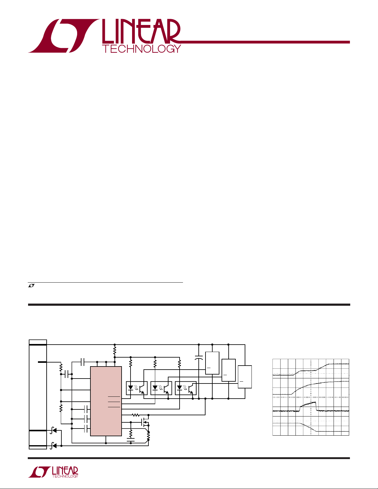
TYPICAL APPLICATIO
–48V/2.5A Hot Swap Controller
–48V RTN
10nF
68nF
0.1µF
0.33µF
1µF
EN2
LTC4253
RESET
UV
OV
SS
SQTIMER
EN3
PWRGD1
PWRGD2
PWRGD3
V
EE
V
IN
DRAIN
GATE
SENSETIMER
–48V RTN
–48V A
–48V B
402k
1%
32.4k
1%
B3100*
B3100*
U
2.5k
15k(1/4W)/6
V
IN
5.6k 5.6k 5.6k
†
1M
IRF530S
10Ω
0.02Ω
18nF
+
100µF
†
*DIODES, INC.
†
MOC207
LOAD1
LOAD2
EN
†
LOAD3
EN
EN
4253 TA01
GATE
10V
SENSE
50mV
V
OUT
50V
SS
1V
Start-Up Behavior
1ms/DIV
4253 TA01b
425353afc
1
LTC4253/LTC4253A
WW
W
U
ABSOLUTE AXI U RATI GS
(Note 1), All voltages referred to V
Current into VIN (100µs Pulse) ........................... 100mA
Current into DRAIN (100µs Pulse)........................ 20mA
V
, DRAIN Minimum Voltage............................... –0.3V
IN
Input/Output (Except SENSE
and DRAIN) Voltage...................................–0.3V to 16V
SENSE Voltage ..........................................–0.6V to 16V
Current Out of SENSE (20µs Pulse) .................. –200mA
Maximum Junction Temperature .......................... 125°C
Operating Temperature Range
LTC4253C/LTC4253AC ............................ 0°C to 70°C
LTC4253I/LTC4253AI ......................... – 40°C to 85°C
Storage Temperature Range ................. –65°C to 150°C
Lead Temperature (Soldering, 10 sec).................. 300°C
EE
UUW
PACKAGE/ORDER I FOR ATIO
ORDER PART
TOP VIEW
1
EN2
PWRGD2
PWRGD1
Order Options Tape and Reel: Add #TR
Lead Free: Add #PBF Lead Free Tape and Reel: Add #TRPBF
Lead Free Part Marking: http://www.linear.com/leadfree/
Consult LTC Marketing for parts specified with wider operating temperature ranges.
2
3
4
V
IN
5
RESET
6
SS
7
SENSE
8
V
EE
16-LEAD PLASTIC SSOP
T
= 125°C, θJA = 130°C/W
JMAX
GN PACKAGE
16
15
14
13
12
11
10
9
PWRGD3
EN3
SQTIMER
TIMER
UV
OV
DRAIN
GATE
NUMBER
LTC4253CGN
LTC4253IGN
LTC4253ACGN
LTC4253AIGN
GN PART
MARKING
4253
4253I
4253A
4253AI
ELECTRICAL CHARACTERISTICS
temperature range, otherwise specifications are at T
SYMBOL PARAMETER CONDITIONS MIN TYP MAX MIN TYP MAX UNITS
V
Z
R
Z
I
IN
V
LKO
V
LKH
V
IH
V
IL
V
HYST
I
RESET
I
EN
V
CB
V
ACL
V
ACL
V
CB
V
FCL
V
SS
I
SS
VIN – VEE Zener Voltage IIN = 2mA
VIN – VEE Zener Dynamic Impedance IIN = (2mA to 30mA) 5 5 Ω
VIN Supply Current UV = OV = 4V, V
V
Undervoltage Lockout Coming Out of UVLO (Rising VIN)
IN
V
Undervoltage Lockout Hysteresis
IN
TTL Input High Voltage
TTL Input Low Voltage
TTL Input Buffer Hysteresis 600 600 mV
RESET Input Current V
EN2, EN3 Input Current VEN = 4V
Circuit Breaker Current Limit Voltage VCB = (V
Analog Current Limit Voltage V
Analog Current Limit Voltage V
Circuit Breaker Current Limit Voltage
Fast Current Limit Voltage V
SS Voltage After End of SS Timing Cycle
SS Pin Current UV = OV = 4V, V
≤ V
EE
VEN = 0V
= (V
ACL
= (V
ACL
= (V
FCL
V
= 0V (Sourcing)
SS
UV = OV = 0V, V
V
= 1V (Sinking)
SS
The ● denotes the specifications which apply over the full operating
= 25°C. (Note 2)
A
LTC4253 LTC4253A
●
11.5 13 14.5 11.5 13 14.5 V
= (VZ – 0.3V)
IN
≤ V
RESET
IN
– VEE)
SENSE
– VEE), SS = Open or 2.2V
SENSE
– VEE), SS = Open or 1.4V
SENSE
– VEE)
SENSE
= V
SENSE
= V
SENSE
EE,
EE,
●
●
●
●
●
●
●
●
●
●
●
●
●
●
0.8 2 1.1 2 mA
9.2 11.5 9 10 V
0.5 1 1.5 0.25 0.5 0.75 V
22 V
0.8 0.8 V
±0.1 ±10 ±0.1 ±10 µA
60 120 180 60 120 180 µA
±0.1 ±10 ±0.1 ±10 µA
40 50 60 45 50 55 mV
80 100 120 mV
1.05 1.20 1.38 V/V
150 200 300 150 200 300 mV
2 2.2 2.4 1.25 1.4 1.55 V
12 22 32 16 28 40 µA
28 28 mA
425353afc
2
LTC4253/LTC4253A
ELECTRICAL CHARACTERISTICS
temperature range, otherwise specifications are at T
The ● denotes the specifications which apply over the full operating
= 25°C. (Note 2)
A
LTC4253 LTC4253A
SYMBOL PARAMETER CONDITIONS MIN TYP MAX MIN TYP MAX UNITS
R
SS
V
OS
V
+ VOSRatio (V
ACL
V
SS
I
GATE
V
GATE
V
GATEL
V
GATEH
SS Output Impedance 100 50 kΩ
Analog Current Limit Offset Voltage 10 10 mV
+ VOS) to SS Voltage 0.05 0.05 V/V
ACL
GATE Pin Output Current UV = OV = 4V, V
= 0V (Sourcing)
V
GATE
UV = OV = 4V, V
V
= 3V (Sinking)
GATE
UV = OV = 4V, V
= 1V (Sinking)
V
GATE
External MOSFET Gate Drive V
GATE
– V
EE, IIN
= VEE,
SENSE
– VEE = 0.15V, 17 17 mA
SENSE
– VEE = 0.3V, 190 190 mA
SENSE
= 2mA
●
30 50 70 30 50 70 µA
●
10 12 V
Z
10 12 V
Z
Gate Low Threshold Before Gate Ramp Up 0.5 0.5 V
Gate High Threshold V
GATEH
= VIN – V
, for PWRGD1, 2.8 2.8 V
GATE
PWRGD2, PWRGD3 Status
V
UVHI
V
UVLO
V
UV
V
UVHST
V
OVHI
V
OVLO
V
OV
V
OVHST
I
SENSE
UV Pin Threshold HIGH UV Low to High
UV Pin Threshold LOW UV High to Low
UV Pin Threshold UV Low to High
●
3.075 3.225 3.375 V
●
2.775 2.925 3.075 V
●
3.05 3.08 3.11 V
UV Pin Hysteresis 230 300 350 mV
OV Pin Threshold HIGH OV Low to High
OV Pin Threshold LOW OV High to Low
OV Pin Threshold OV Low to High
●
●
5.85 6.15 6.45 V
●
5.55 5.85 6.15 V
●
292 324 356 mV
5.04 5.09 5.14 V
OV Pin Hysteresis 230 300 350 mV
SENSE Pin Input Current UV = 0V = 4V, V
SENSE
= 50mV
●
●
15 30 15 30 µA
82 102 122 mV
(Sourcing)
I
V
V
I
INP
TMR
TMRH
TMRL
UV, OV Pin Input Current UV = OV = 4V
TIMER Pin Voltage High Threshold
TIMER Pin Voltage Low Threshold
TIMER Pin Current Timer On (Initial Cycle/Latchoff,
Sourcing), V
TMR
= 2V
●
●
●
●
±0.1 ± 1 ±0.1 ±1 µA
3.5 4 4.5 3.5 4 4.5 V
0.8 1 1.2 0.8 1 1.2 V
357 357 µA
Timer Off (Initial Cycle, Sinking), 28 28 mA
V
= 2V
TMR
Timer On (Circuit Breaker, Sourcing,
I
DRN
= 0µA), V
TMR
= 2V
●
120 200 280 120 200 280 µA
Timer On (Circuit Breaker, Sourcing, 600 600 µA
I
∆I
TMRACCITMR
∆I
DRN
V
SQTMRH
V
SQTMRL
= 50µA), V
DRN
Timer Off (Circuit Breaker, Sinking),
= 2V
V
TMR
at I
= 50µA – I
DRN
50µAI
TMR
at I
= 0µA Timer On (Circuit Breaker with
DRN
DRN
= 50µA)
SQTIMER Pin Voltage High Threshold
SQTIMER Pin Voltage Low Threshold 0.33 0.33 V
TMR
= 2V
●
357 357 µA
●
789 789µA/µA
●
3.5 4 4.5 3.5 4 4.5 V
V
425353afc
3
LTC4253/LTC4253A
ELECTRICAL CHARACTERISTICS
temperature range, otherwise specifications are at T
The ● denotes the specifications which apply over the full operating
= 25°C. (Note 2)
A
LTC4253 LTC4253A
SYMBOL PARAMETER CONDITIONS MIN TYP MAX MIN TYP MAX UNITS
I
SQTMR
SQTIMER Pin Current SQTIMER On (Power Good
Sequence, Sourcing), V
SQTMR
= 2V
●
357 357 µA
SQTIMER Off (Power Good 28 28 mA
V
DRNL
I
DRNL
V
DRNCL
V
PGL
I
PGH
Sequence, Sinking), V
DRAIN Pin Voltage Low Threshold For PWRGD1, PWRGD2, PWRGD3 Status
DRAIN Leakage Current V
DRAIN Pin Clamp Voltage I
= 5V ±0.1 ±1 µA
DRAIN
= 4V ±0.1 ± 1 µA
V
DRAIN
= 50µA
DRN
PWRGD1, PWRGD2, PWRGD3 IPG = 1.6mA
Output Low Voltage I
= 5mA
PG
PWRGD1, PWRGD2, PWRGD3 VPG = 0V (Sourcing)
SQTMR
= 2V
●
2 2.39 3 2 2.39 3 V
●
6 7 8.5 5 6 7.5 V
●
●
●
0.25 0.4 0.25 0.4 V
1.2 1.2 V
30 50 70 30 50 70 µA
Output High Current
t
SQ
t
SS
t
PLLUG
t
PHLOG
SQTIMER Default Ramp Period SQTIMER Pin Floating, 250 250 µs
V
Ramps from 0.5V to 3.5V
SQTMR
SS Default Ramp Period SS Pin Floating, VSS Ramps from 0.2V to 2V 250 µs
SS Pin Floating, V
UV Low to GATE Low
OV High to GATE Low
Ramps from 0.2V to 1.25V 140 µs
SS
●
●
0.4 5 0.4 5 µs
0.4 5 0.4 5 µs
Note 1: Stresses beyond those listed under Absolute Maximum Ratings
may cause permanent damage to the device. Exposure to any Absolute
Maximum Rating condition for extended periods may affect device
Note 2: All currents into device pins are positive; all currents out of device
pins are negative. All voltages are referenced to V
specified.
reliability and lifetime.
UW
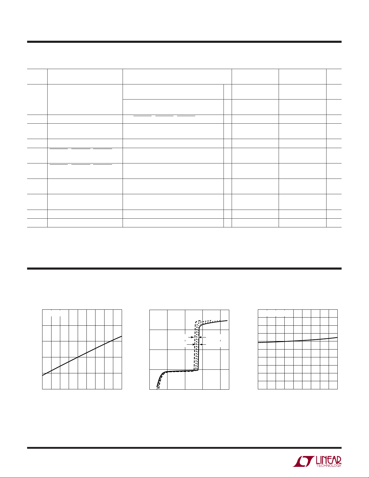
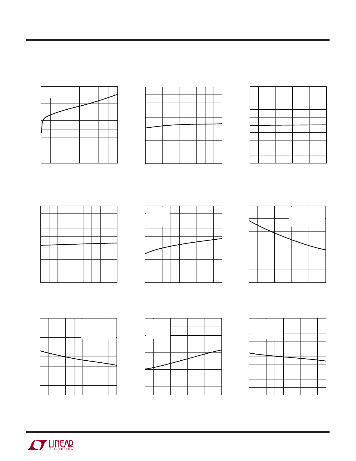
TYPICAL PERFOR A CE CHARACTERISTICS
I
1000
100
(mA)
IN
I
0.1
vs V
IN
IN
TA = –40°C
10
1
0
TA = 25°C
5 10 15 20
VIN (V)
TA = 85°C
TA = 125°C
VZ vs Temperature
14.5
IIN = 2mA
14.0
13.5
(V)
Z
V
13.0
12.5
12.0
–55 –35 –15 5 25 45 65 85 105 125
TEMPERATURE (°C)
4253 G01
4253 G02
unless otherwise
EE
I
vs Temperature
IN
1000
VIN = VZ – 0.3V
950
900
850
800
750
(µA)
IN
I
700
650
600
550
500
–55 –35 –15 5 25 45 65 85 105 125
TEMPERATURE (°C)
4253 G03
4
425353afc
UW
TYPICAL PERFOR A CE CHARACTERISTICS
LTC4253/LTC4253A
vs V
EN
EN
180
IIN = 2mA
= 25°C
T
160
A
140
120
100
(µA)
EN
80
I
60
40
20
0
02
4 6 8 10 12 14 16
VEN (V)
Fast Current Limit Voltage V
Temperature
300
280
260
240
220
(mV)
200
FCL
V
180
160
140
120
100
–55 –35 –15 5 25 45 65 85 105 125
TEMPERATURE (°C)
FCL
4253 G04
vs
4253 G07
Circuit Breaker Current Limit
Voltage V
55
54
53
52
51
(mV)
50
CB
V
49
48
47
46
45
–55 –35 –15 5 25 45 65 85 105 125
I
GATE
60
UV/OV = 4V
58
TIMER = 0V
V
SENSE
56
V
GATE
54
52
(µA)
50
GATE
I
48
46
44
42
40
–55 –35 –15 5 25 45 65 85 105 125
vs TemperatureI
CB
TEMPERATURE (°C)
(Source) vs Temperature I
= V
EE
= 0V
TEMPERATURE (°C)
4253 G05
4253 G08
Analog Current Limit Voltage V
vs Temperature
150
140
130
120
110
(mV)
100
ACL
V
90
80
70
60
50
–55 –35 –15 5 25 45 65 85 105 125
GATE
30
25
20
(mA)
15
GATE
I
10
5
0
–55 –35 –15 5 25 45 65 85 105 125
TEMPERATURE (°C)
(ACL, Sink) vs Temperature
UV/OV = 4V
TIMER = 0V
– VEE = 0.15V
V
SENSE
= 3V
V
GATE
TEMPERATURE (°C)
ACL
4253 G06
4253 G09
I
(FCL, Sink) vs Temperature V
GATE
400
350
300
250
(mA)
200
GATE
I
150
100
50
0
–55 –35 –15 5 25 45 65 85 105 125
TEMPERATURE (°C)
UV/OV = 4V
TIMER = 0V
– VEE = 0.3V
V
SENSE
= 1V
V
GATE
4253 G10
vs Temperature V
GATE
14.5
UV/OV = 4V
TIMER = 0V
(V)
GATE
V
14.0
13.5
13.0
12.5
12.0
11.5
11.0
10.5
10.0
= V
V
SENSE
IIN = 2mA
–55 –35 –15 5 25 45 65 85 105 125
EE
TEMPERATURE (°C)
4253 G11
vs Temperature
GATEL
1.0
UV/OV = 4V
0.9
TIMER = 0V
GATE THRESHOLD
0.8
BEFORE RAMP UP
0.7
0.6
(V)
0.5
GATEL
V
0.4
0.3
0.2
0.1
0
–55 –35 –15 5 25 45 65 85 105 125
TEMPERATURE (°C)
4253 G12
425353afc
5
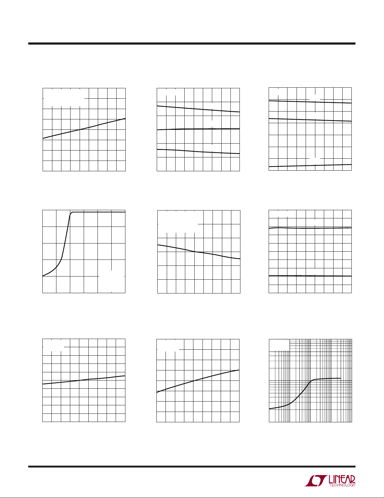
LTC4253/LTC4253A
UW
TYPICAL PERFOR A CE CHARACTERISTICS
vs Temperature
GATEH
3.6
UV/OV = 4V
= VIN – V
V
GATEH
3.4
IIN = 2mA
3.2
3.0
(V)
2.8
GATEH
V
2.6
2.4
2.2
2.0
–55 –35 –15 5 25 45 65 85 105 125
SENSE
0.01
0.1
1
(mA)
SENSE
10
–I
100
1000
–1.5
–1 –0.5 0 0.5 1 1.5
GATE
TEMPERATURE (°C)
vs (V
SENSE
V
SENSE
– VEE)
– VEE (V)
UV/OV = 4V
TIMER = 0V
GATE = HIGH
= 25°C
T
A
4253 G13
4253 G16
3.375
IIN = 2mA
3.275
3.175
3.075
2.975
UV THRESHOLD (V)
2.875
2.775
–55 –35 –15 5 25 45 65 85 105 125
SENSE
0
UV/OV = 4V
TIMER = 0V
V
–5
V
–10
(µA)
–15
SENSE
I
–20
–25
–30
–55 –35 –15 5 25 45 65 85 105 125
SENSE
GATE
= HIGH
vs TemperatureI
– VEE = 50mV
TEMPERATURE (°C)
TEMPERATURE (°C)
V
UVH
V
UV
V
UVL
4253 G14
4253 G17
Threshold vs TemperatureUV Threshold vs TemperatureV
OV
6.4
IIN = 2mA
6.2
6.0
5.8
5.6
OV THRESHOLD (V)
5.4
5.2
5.0
–55 –35
–15
V
OVH
V
OVL
V
OV
45 125
525
TEMPERATURE (°C)
65 85 105
TIMER Threshold vs TemperatureI
5.0
IIN = 2mA
4.5
4.0
3.5
3.0
2.5
2.0
1.5
TIMER THRESHOLD (V)
1.0
0.5
0
–55 –35 –15 5 25 45 65 85 105 125
V
TMRH
V
TMRL
TEMPERATURE (°C)
4352 G15
4253 G18
I
(Initial Cycle, Sourcing)
TMR
vs Temperature
10
IIN = 2mA
9
= 2V
V
TMR
8
7
6
(µA)
5
TMR
I
4
3
2
1
0
–55 –35 –15 5 25 45 65 85 105 125
TEMPERATURE (°C)
6
4253 G19
I
(Circuit Breaker, Sourcing)
TMR
vs Temperature
240
IIN = 2mA
= 0µA
I
DRN
230
220
210
(µA)
200
TMR
I
190
180
170
160
–55 –35 –15 5 25 45 65 85 105 125
TEMPERATURE (°C)
4253 G20
10
(mA)
TMR
I
0.1
I
1
0.001
vs I
TMR
IIN = 2mA
T
DRN
= 25°C
A
0.01 0.1 110
I
(mA)
DRN
4253 G21
425353afc

UW
TEMPERATURE (°C)
–55 –35 –15 5 25 45 65 85 105 125
V
PGL
(V)
4253 G27
3.0
2.5
2.0
1.5
1.0
0.5
0
IIN = 2mA
IPG = 10mA
IPG = 5mA
IPG = 1.6mA
TEMPERATURE (°C)
–55 –35 –15 5 25 45 65 85 105 125
t
SQ
(µs)
4253 G30
500
450
400
350
300
250
200
150
100
50
0
IIN = 2mA
V
SQTMR
RAMPS FROM 0.5V TO 3.5V
TYPICAL PERFOR A CE CHARACTERISTICS
SQTIMER Threshold
∆I
9.0
IIN = 2mA
8.8
8.6
8.4
(µA/µA)
8.2
DRN
8.0
∆I
7.8
7.6
TMRACC/
∆I
7.4
7.2
7.0
–55 –35 –15 5 25 45 65 85 105 125
V
8.0
IIN = 2mA
7.8
I
DRN
7.6
7.4
7.2
(V)
7.0
DRNCL
6.8
V
6.6
6.4
6.2
6.0
–55 –35 –15 5 25 45 65 85 105 125
/∆I
TMRACC
TEMPERATURE (°C)
vs Temperature
DRNCL
= 50µA
TEMPERATURE (°C)
vs Temperature
DRN
4253 G22
4253 G25
vs Temperature
5.0
IIN = 2mA
4.5
4.0
3.5
3.0
(V)
2.5
SQTMR
2.0
V
1.5
1.0
0.5
0
–55 –35 –15 5 25 45 65 85 105 125
I
DRN
100
IIN = 2mA
10
1
0.1
(mA)
0.01
DRN
I
TA = 125°C
0.001
0.0001
0.00001
0
TEMPERATURE (°C)
vs V
DRAIN
TA = 85°C
TA = –40°C
2 4 6 8 10 12 14 16
V
DRAIN
V
SQTMRH
V
SQTMRL
TA = 25°C
(V)
LTC4253/LTC4253A
vs Temperature
V
DRNL
2.60
IIN = 2mA
2.55
2.50
2.45
(V)
2.40
DRNL
V
2.35
2.30
2.25
2.20
4253 G23
4253 G26
–55 –35 –15 5 25 45 65 85 105 125
V
PGL
TEMPERATURE (°C)
vs Temperature
4253 G24
vs Temperature
I
PGH
60
IIN = 2mA
58
56
54
52
(µA)
50
PGH
V
48
46
44
42
40
–55 –35 –15 5 25 45 65 85 105 125
= 0V
V
PWRGD
TEMPERATURE (°C)
4253 G28
t
vs Temperature
SS
300
IIN = 2mA
290
SS PIN FLOATING
RAMPS FROM 0.2V TO 2V
V
SS
280
270
260
(µs)
250
SS
t
240
230
220
210
200
–55 –35 –15 5 25 45 65 85 105 125
TEMPERATURE (°C)
4253 G29
t
vs Temperature
SQ
425353afc
7
LTC4253/LTC4253A
UUU
PI FU CTIO S
EN2 (Pin 1): Power Good Status Output Two Enable. This
is a TTL compatible input that is used to control PWRGD2
and PWRGD3 outputs. When EN2 is driven low, both
PWRGD2 and PWRGD3 will go high. When EN2 is driven
high, PWRGD2 will go low provided PWRGD1 has been
active for more than one power good sequence delay
) provided by the sequencing timer. EN2 can be used
(t
SQT
to control the power good sequence. This pin is internally
pulled low by a 120µA current source.
PWRGD2 (Pin 2): Power Good Status Output Two. Power
good sequence starts with PWRGD1 latching active low.
PWRGD2 will latch active low after EN2 goes high and after
one power good sequence delay t
provided by the
SQT
sequencing timer from the time PWRGD1 goes low,
whichever comes later. PWRGD2 is reset by PWRGD1
going high or EN2 going low. This pin is internally pulled
high by a 50µA current source.
PWRGD1 (Pin 3): Power Good Status Output One. At
start-up, PWRGD1 latches active low and starts the power
good sequence when the DRAIN pin is below 2.39V and
GATE is within 2.8V of VIN. PWRGD1 status is reset by UV,
VIN (UVLO), RESET going high or circuit breaker fault
time-out. This pin is internally pulled high by a 50µA
current source.
V
(Pin 4): Positive Supply Input. Connect this pin to the
IN
positive side of the supply through a dropping resistor. A
shunt regulator clamps VIN at 13V above VEE. An internal
undervoltage lockout (UVLO) circuit holds GATE low until
the V
pin is greater than V
IN
UV is high, OV is low and V
, overriding UV and OV. If
LKO
comes out of UVLO, TIMER
IN
starts an initial timing cycle before initiating GATE ramp
up. If V
drops below approximately 8.2V (8.5V for the
IN
LTC4253A), GATE pulls low immediately.
RESET (Pin 5): Circuit Breaker Reset Pin. This is an
asynchronous TTL compatible input. RESET going high
will pull GATE, SS, TIMER, SQTIMER low and the PWRGD
outputs high. The RESET pulse must be wide enough to
discharge any voltage on the TIMER pin below V
TMRL
.
After the reset of a latched fault, the chip waits for the
interlock conditions before recovering as described in
Interlock Conditions in the Operation section.
SS (Pin 6): Soft-Start Pin. This pin is used to ramp inrush
current during start up, thereby effecting control over
di/dt. A 20X attenuated version of the SS pin voltage is
presented to the current limit amplifier. This attenuated
voltage limits the MOSFET’s drain current through the
sense resistor during the soft-start current limiting. At the
beginning of the start-up cycle, the SS capacitor (C
SS
) is
ramped by a 22µA (28µA for the LTC4253A) current
source. The GATE pin is held low until SS exceeds 20 • V
= 0.2V. SS is internally shunted by a 100k R
which limits
SS
OS
the SS pin voltage to 2.2V (50k resistor and 1.4V for the
LTC4253A). This corresponds to an analog current limit
SENSE voltage of 100mV (60mV for the LTC4253A). If the
SS capacitor is omitted, the SS pin ramps up in about
250µs (140µs for the LTC4253A). The SS pin is pulled low
under any of the following conditions: UVLO at V
, UV,
IN
OV, during the initial timing cycle, a circuit breaker fault
time-out or the RESET pin going high.
SENSE (Pin 7): Circuit Breaker/Current Limit Sense Pin.
Load current is monitored by a sense resistor R
nected between
SENSE and VEE, and controlled in three
con-
S
steps. If SENSE exceeds VCB (50mV), the circuit breaker
comparator activates a (200µA+8•I
current. If SENSE exceeds V
, the analog current-limit
ACL
) TIMER pull-up
DRN
amplifier pulls GATE down to regulate the MOSFET current
at V
SENSE may overshoot V
. In the event of a catastrophic short-circuit,
ACL/RS
. If SENSE reaches V
ACL
FCL
(200mV), the fast current-limit comparator pulls GATE
low with a strong pull-down. To disable the circuit breaker
and current limit functions, connect SENSE to VEE.
VEE (Pin 8): Negative Supply Voltage Input. Connect this
pin to the negative side of the power supply.
GATE (Pin 9): N-channel MOSFET Gate Drive Output. This
pin is pulled high by a 50µA current source. GATE is pulled
low by invalid conditions at VIN (UVLO), UV, OV, during the
initial timing cycle, a circuit breaker fault time-out or the
RESET pin going high. GATE is actively servoed to control
the fault current as measured at SENSE. Compensation
capacitor, CC, at GATE stabilizes this loop. A comparator
monitors GATE to ensure that it is low before allowing an
initial timing cycle, then the GATE ramps up after an
overvoltage event or restart after a current limit fault.
8
425353afc

UUU
PI FU CTIO S
LTC4253/LTC4253A
During GATE start-up, a second comparator detects GATE
within 2.8V of V
before PWRGD1 can be set and power
IN
good sequencing starts.
DRAIN (Pin 10): Drain Sense Input. Connecting an external resistor, RD between this pin and the MOSFET’s drain
) allows voltage sensing below 6.15V (5V for
(V
OUT
LTC4253A) and current feedback to TIMER. A comparator
detects if DRAIN is below 2.39V and together with the
GATE high comparator, sets the PWRGD1 flag. If V
above V
V
DRNCL
, the DRAIN pin is clamped at approximately
DRNCL
. RD current is internally multiplied by 8 and added
OUT
is
to TIMER’s 200µA during a circuit breaker fault cycle. This
reduces the fault time and MOSFET heating.
OV (Pin 11): Overvoltage Input. For the LTC4253, the
threshold at the OV pin is set at 6.15V with 0.3V hysteresis.
If OV > 6.15V, GATE pulls low. When OV returns below
5.85V, GATE start-up begins without an initial timing
cycle. The LTC4253A OV threshold is set at 5.09V with
102mV hysteresis. If OV > 5.09V, GATE pulls low. When
OV returns below 4.988V, GATE start-up begins without
an initial timing cycle. If OV occurs in the middle of an
initial timing cycle, the initial timing cycle is restarted after
OV goes away. OV does not reset the latched fault or
PWRGD1 flag. The internal UVLO at V
always overrides
IN
OV. A 1nF to 10nF capacitor at OV prevents transients and
switching noise from affecting the OV thresholds and
prevents glitches at the GATE.
starts an initial timing cycle when the following conditions
are met: RESET is low, UV is high, OV is low, V
UVLO, TIMER pin is low, GATE pin is lower than V
< 0.2V, and V
then charges C
(4V), the timing cycle terminates. TIMER quickly
V
TMRH
– VEE < VCB. A pull-up current of 5µA
SENSE
, generating a time delay. If CT charges to
T
clears
IN
GATEL
, SS
pulls low and GATE is activated.
If SENSE exceeds 50mV while GATE is high, a circuit
breaker cycle begins with a 200µA pull-up current charg-
ing C
. If DRAIN is approximately 7V (6V for the LTC4253A)
T
during this cycle, the timer pull-up has an additional
current of 8 • I
. If SENSE drops below 50mV before
DRN
TIMER reaches 4V, a 5µA pull-down current slowly dis-
charges the C
up to the V
. In the event that CT eventually integrates
T
(4V) threshold, the circuit breaker trips,
TMRH
GATE quickly pulls low and PWRGD1 pulls high. TIMER
latches high with a 5µA pull-up source. This latched fault
may be cleared by driving RESET high until TIMER is
pulled low. Other ways of clearing the fault include pulling
the V
pin momentarily below (V
IN
LKO
– V
), pulling
LKH
TIMER low with an external device or pulling UV below
2.925V (2.756V for the LTC4253A).
SQTIMER (Pin 14): Sequencing Timer Input. The sequencing timer provides a delay t
for the power good sequenc-
SQT
ing. This delay is adjusted by connecting an appropriate
capacitor to this pin. If the SQTIMER capacitor is omitted,
the SQTIMER pin ramps from 0V to 4V in about 300µs.
UV (Pin 12): Undervoltage Input. For the LTC4253, the
threshold at the UV pin is set at 3.225V with 0.3V hysteresis. If UV < 2.925V, PWRGD1 pulls high, both GATE and
TIMER pull low. If UV rises above 3.225V, this initiates an
initial timing cycle followed by GATE start-up. The
LTC4253A UV threshold is set at 3.08V with 324mV
hysteresis. If UV < 2.756V, PWRGD1 pulls high, both
GATE and TIMER pull low. If UV rises above 3.08V, this
initiates an initial timing cycle followed by GATE start-up.
The internal UVLO at V
always overrides UV. A low at UV
IN
resets an internal fault latch. A 1nF to 10nF capacitor at UV
prevents transients and switching noise from affecting the
UV thresholds and prevents glitches at the GATE pin.
TIMER (Pin 13): Timer Input. Timer is used to generate an
initial timing delay at start-up, and to delay shutdown in the
event of an output overload (circuit breaker fault). Timer
EN3 (Pin 15): Power Good Status Output Three Enable.
This is a TTL compatible input that is used to control the
PWRGD3 output. When EN3 is driven low, PWRGD3 will
go high. When EN3 is driven high, PWRGD3 will go low
provided PWRGD2 has been active for for more than one
power good sequence delay (t
). EN3 can be used to
SQT
control the power good sequence. This pin is internally
pulled low by a 120µA current source.
PWRGD3 (Pin 16): Power Good Status Output Three.
Power good sequence starts with PWRGD1 latching active
low. PWRGD3 will latch active low after EN3 goes high and
after one power good sequence delay t
provided by the
SQT
sequencing timer from the time PWRGD2 goes low,
whichever comes later. PWRGD3 is reset by PWRGD1
going high or EN3 going low. This pin is internally pulled
high by a 50µA current source.
425353afc
9
LTC4253/LTC4253A
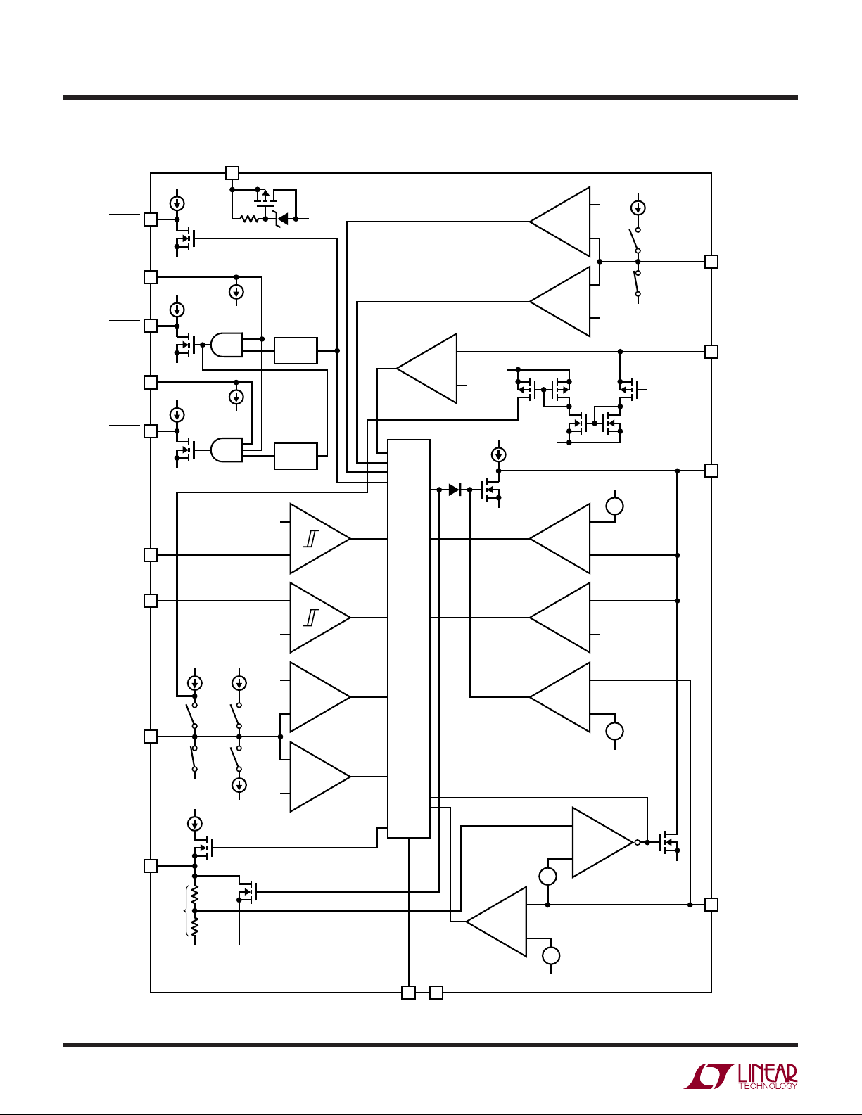
W
BLOCK DIAGRA
V
IN
50µA
50µA
50µA
120µA
120µA
4
V
EE
SQTIMER
DELAY
V
EE
SQTIMER
DELAY
6.15V
(5.09V)
PWRGD1
EN2
PWRGD2
EN3
PWRGD3
V
IN
3
V
EE
1
V
IN
2
V
EE
15
V
IN
16
V
EE
11
OV
V
IN
–
V
EE
4V
5µA
+
SQTIMER
14
–
V
EE
0.33V
+
DRAIN
–
V
IN
2.39V
+
–
+
8× 1×
V
IN
V
EE
V
50µA
6.15V
(5V)
1×
EE
–
1×
V
IN
+
2.8V
–
+
10
GATE
9
UV 12
(2.756V)
V
IN
200µA
V
IN
5µA
2.925V
–
+
–
4V
+
TIMER 13
–
V
EE
V
IN
22µA
(28µA)
SS 6
95k
(47.5k)
R
SS
5k
(2.5k)
V
EE
FOR COMPONENTS, CURRENTS AND VOLTAGES WITH TWO
VALUES, VALUES WITHOUT PARENTHESES REFER TO THE
LTC4253, VALUES WITH PARENTHESES REFER TO THE LTC4253A
5µA
1V
V
EE
V
EE
+
LOGIC
5
RESET
–
0.5V
+
+
FCL
–
+
200mV
–
V
EE
+
ACL
–
+
10mV
–
+
CB
V
EE
SENSE7
–
+
50mV
–
V
8
V
EE
EE
4253 BD
425353afc
10
 Loading...