

FEATURES
■
Controls –12V, 3.3V, 5V and 12V Supplies
■
±14.4V Absolute Maximum Rating for 12V
IN
and –12VIN Input Pins
■
Insensitive to Supply Voltage Transients
■
Adjustable Foldback Current Limit with Circuit Breaker
■
LOCAL_PCI_RST# Logic On-Chip
■
PRECHARGE Output Biases I/O Pins During Card
Insertion and Extraction
■
LTC4244-1 Designed for Applications without –12V
■
Available in 20-Lead Narrow SSOP Package
U
APPLICATIO S
■ Hot Board Insertion into CompactPCI Bus
, LTC and LT are registered trademarks of Linear Technology Corporation.
Hot Swap is a trademark of Linear Technology Corporation.
CompactPCI is a trademark of the PCI Industrial Computer Manufacturers Group.
LTC4244/LTC4244-1
Rugged, CompactPCI Bus
Hot Swap Controllers
U
DESCRIPTIO
The LTC®4244/LTC4244-1 are Hot SwapTM controllers that
allow a board to be safely inserted into and removed from
a CompactPCITM bus slot. External N-channel transistors
control the 5V and 3.3V supplies while on-chip switches
control the ±12V supplies. The 3.3V and 5V supplies can
be ramped up at an adjustable rate. Electronic circuit
breakers protect all four supplies against overcurrent
faults. After the power-up cycle is complete, the TIMER pin
capacitor serves as auxiliary VCC allowing the LTC4244/
LTC4244-1 to function without interruption in the presence of voltage spikes on the 12VIN supply. The PWRGD
output indicates when all four supplies are within tolerance. The OFF/ON pin is used to cycle board power or reset
the circuit breaker. The PRECHARGE output can be used
to bias the bus I/O pins during card insertion and extraction. PCI_RST# is combined on-chip with HEALTHY# in
order to generate LOCAL_PCI_RST#.
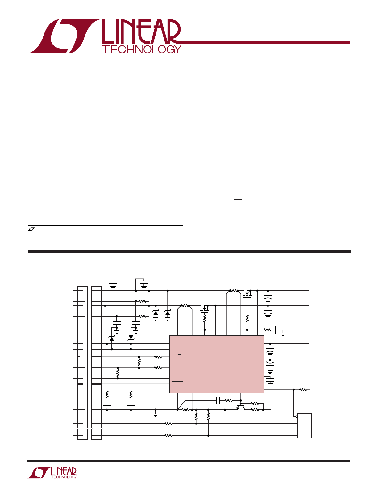
TYPICAL APPLICATIO
5V
LONG 5V
3.3V
LONG 3.3V
12V
–12V
BD_SEL#
LONG V(I/O)
HEALTHY#
PCI_RST#
R15
1Ω
C4
GROUND
I/O PIN 1
I/O PIN 128
•
•
•
0.01µF
I/O DATA LINE 1
I/O DATA LINE 128
Z1, Z2: SMAJ12A Z3, Z4: SMAJ5.0A
U
C8
0.01µF PER
POWER PIN
C6
0.01µF
R17
10k
Z2Z1
R16
1Ω
C5
0.01µF
R22
2.7Ω
R21
1.8Ω
C7
0.01µF
R20
1.2k
C9
0.01µF PER
POWER PIN
R19 1k
R18 10k
•
•
•
3.3V
Z3
5V
IN
IN
Z4
3.3V
12V
V
EEIN
OFF/ON
FAULT
PWRGD
RESETIN
GND PRECHARGE
R13
10Ω
R14
10Ω
0.005Ω
IN
IN
R10 18Ω
R1
Q1
IRF7457
R3
10Ω
3.3V
SENSE
3.3V
GATE 5V
LTC4244
C3 4.7nF
R12
R11
10k
10k
OUT
5V
IN5VSENSE
R9 24Ω
1V
±10%
R2
0.007Ω
DRIVE
MMBT2222A
IRF7457
Q3
Q2
R4
10Ω
12V
V
TIMER
RESETOUT
R8 1k
R7 12Ω
OUT
OUT
EEOUT
•
•
•
+
C
LOAD(5VOUT)
+
C
LOAD(3.3VOUT)
C1
R5
0.33µF
1k
+
C
LOAD(12VOUT)
C
LOAD(VEEOUT)
+
C2
0.082µF
LOCAL_PCI_RST#
V
IN
3.3V
I/O #1
I/O #128
R6
10k
RESET#
PCI
BRIDGE
CHIP
4244 F01
V
OUT
5V
5A
V
OUT
3.3V
7A
V
OUT
12V
500mA
V
EEOUT
–12V
100mA
V
OUT
3.3V
Figure 1. Typical Compact PCI Application
42441f
1
LTC4244/LTC4244-1
WWWU
ABSOLUTE AXI U RATI GS
(Notes 1, 2, 3)
Supply Voltages
12VIN................................................................ 14.4V
V
.............................................................. –14.4V
EEIN
Input Voltages (OFF/ON, RESETIN) ........–0.3V to 13.5V
Output Voltages (FAULT, PWRGD, RESETOUT)
...........................................................–0.3V to 13.5V
Analog Voltages and Currents
5V
, DRIVE, 5VIN, 3.3V
OUT
...........................................................–0.3V to 13.5V
PRECHARGE, GATE ....................................... ±20mA
V
TIMER, 12V
................................................–14.4V to 0.3V
EEOUT
...........................................
OUT
Operation Temperature Range
LTC4244C/LTC4244C-1........................... 0°C to 70°C
LTC4244I/LTC4244I-1 ........................ –40°C to 85°C
Storage Temperature Range ................. –65°C to 150°C
Lead Temperature (Soldering, 10 sec).................. 300°C
, 3.3VIN, 3.3V
SENSE
, 5V
OUT
SENSE
–0.3V to 14.4V
UU
W
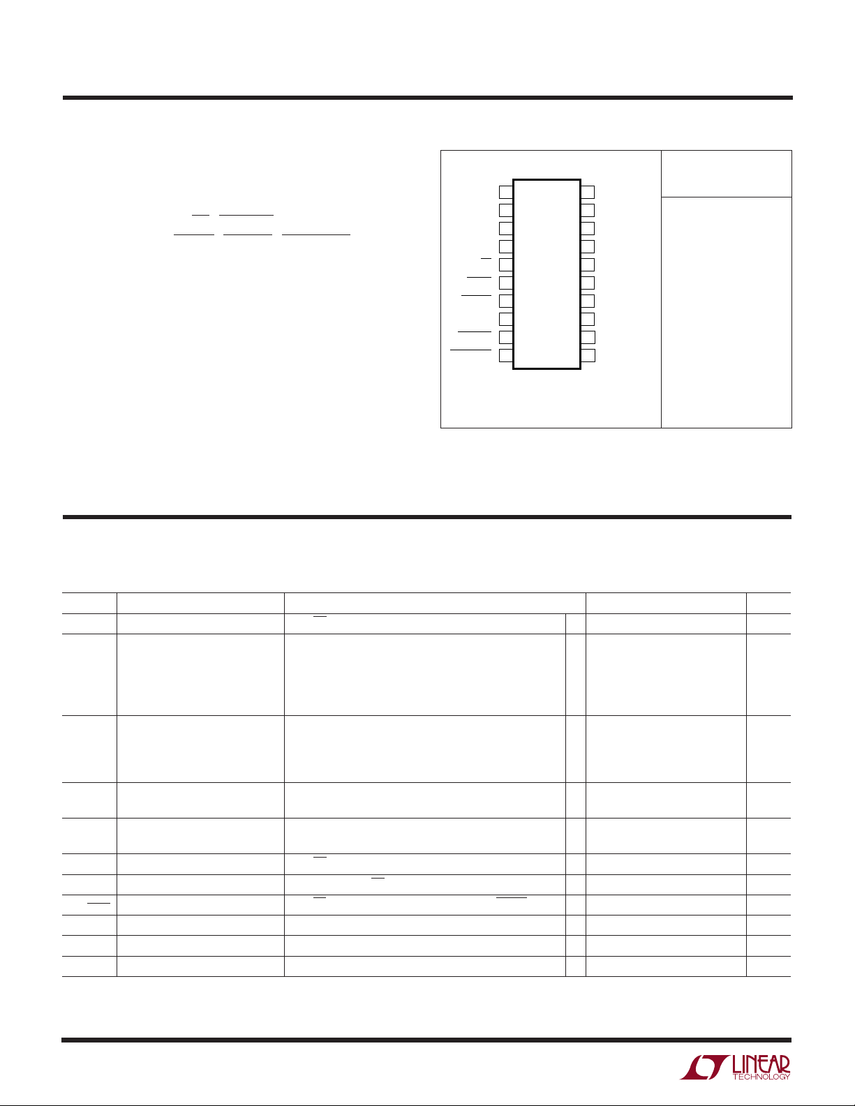
PACKAGE/ORDER I FOR ATIO
TOP VIEW
1
12V
V
EEIN
5V
OUT
TIMER
OFF/ON
FAULT
PWRGD
GND
RESETIN
RESETOUT
IN
2
3
4
5
6
7
8
9
10
GN PACKAGE
20-LEAD PLASTIC SSOP
T
= 140°C, θJA = 135°C/W
JMAX
12V
20
V
19
3.3V
18
3.3V
17
3.3V
16
GATE
15
5V
14
13
5V
12
PRECHARGE
11
DRIVE
OUT
EEOUT
OUT
IN
SENSE
SENSE
IN
Consult LTC Marketing for parts specified with wider operating temperature ranges.
ORDER PART
NUMBER
LTC4244CGN
LTC4244CGN-1
LTC4244IGN
LTC4244IGN-1
ELECTRICAL CHARACTERISTICS
temperature range, otherwise specifications are at TA = 25°C. V
The ● denotes the specifications which apply over the full operating
12VIN
= 12V, V
= –12V, V
EEIN
3.3VIN
= 3.3V, V
= 5V, unless
5VIN
otherwise noted.
SYMBOL PARAMETER CONDITIONS MIN TYP MAX UNITS
I
DD
V
LKO
V
FB
V
CB
t
OC
I
GATE(UP)
I
GATE(DN)
I
GATE(FAULT)
∆V
GATE
∆V
12V
∆V
VEE
V
Supply Current OFF/ON = 0V ● 410 mA
12VIN
Undervoltage Lockout 12VIN, Ramping Down ● 8 9 10 V
, Ramping Down ● 4 4.25 4.5 V
5V
IN
3.3V
, Ramping Down ● 2.25 2.5 2.75 V
IN
, Ramping Up (LTC4244 Only) ● –8.25 –9.25 –10.25 V
V
EEIN
TIMER, Ramping Down, V
Foldback Current Limit Voltage VFB = (V
V
FB
V
FB
V
FB
Circuit Breaker Trip Voltage VCB = (V
V
CB
Overcurrent Fault Response Time (V
(V
5VIN
3.3VIN
= (V
= (V
= (V
= (V
– V
– V
5VIN
5VIN
3.3VIN
3.3VIN
5VIN
3.3VIN
5VSENSE
3.3VSENSE
– V
– V
– V
– V
– V
– V
GATE Pin Output Current OFF/ON = 0V, V
V
= 5V, OFF/ON = 4V ● 20 60 100 µA
GATE
OFF/ON = 0V, V
External Gate Voltage ∆V
Internal Switch Voltage Drop ∆V
∆V
GATE
12V
VEE
= (V
= (V
= (V
12VIN
12VIN
EEOUT
5VSENSE
5VSENSE
3.3VSENSE
3.3VSENSE
5VSENSE
3.3VSENSE
) = 100mV, TIMER = FLOAT ● 17 25 35 µs
) = 100mV, TIMER = FLOAT ● 17 25 35 µs
= 2V, TIMER = 0V ● –20 –67 –100 µA
GATE
= 2V, TIMER = FLOAT, FAULT = 0V ● 4 8 16 mA
GATE
– V
GATE
– V
12VOUT
– V
EEIN
= 6V ● 8.25 9.25 10.25 V
12VIN
), V
), V
= 0V, TIMER = 0V ● 11 16 21 mV
5VOUT
= 3V, TIMER = 0V ● 46 51 56 mV
5VOUT
), V
), V
= 0V, TIMER = 0V ● 11 16 21 mV
3.3VOUT
= 2V, TIMER = 0V ● 46 51 56 mV
3.3VOUT
), TIMER = FLOAT ● 45 52 57 mV
), TIMER = FLOAT ● 45 52 57 mV
), I
= –1µA ● 0.6 1 V
GATE
), I = 500mA ● 225 600 mV
), IEE = 100mA ● 110 250 mV
2
42441f
LTC4244/LTC4244-1
ELECTRICAL CHARACTERISTICS
temperature range, otherwise specifications are at TA = 25°C. V
The ● denotes the specifications which apply over the full operating
12VIN
= 12V, V
= –12V, V
EEIN
3.3VIN
= 3.3V, V
= 5V, unless
5VIN
otherwise noted.
SYMBOL PARAMETER CONDITIONS MIN TYP MAX UNITS
I
CL
T
TS
V
TH
V
IL
V
IH
I
IN
I
TIMER
V
TIMER
∆V
R
DIS
V
OL
V
PXG
Note 1: Absolute Maximum Ratings are those values beyond which the life
of a device may be impaired.
Note 2: All currents into device pins are positive; all currents out of device
pins are negative. All voltages are referenced to ground unless otherwise
specified.
Current Foldback 12VIN = 12V, 12V
= 12V, 12V
12V
IN
V
= –12V, V
EEIN
= –12V, V
V
EEIN
= 0V, TIMER = 0V ● –100 –360 –1000 mA
OUT
= 10V, TIMER = 0V ● –550 –850 –1500 mA
OUT
= 0V, TIMER = 0V ● 50 225 350 mA
EEOUT
= –10V, TIMER = 0V ● 350 610 870 mA
EEOUT
Thermal Shutdown Temperature Junction Temperature, Ramping Up 150 °C
Power Good Threshold Voltage 12V
, Ramping Down ● 10.8 11.1 11.4 V
OUT
, Ramping Down ● 4.50 4.61 4.75 V
5V
OUT
3.3V
, Ramping Down ● 2.80 2.90 3.00 V
OUT
, Ramping Up, LTC4244 Only ● –10.8 –11.1 –11.4 V
V
EEOUT
Logic Input Low Voltage OFF/ON, RESETIN, FAULT ● 0.8 V
Logic Input High Voltage OFF/ON, RESETIN, FAULT ● 2V
OFF/ON, RESETIN Input Current OFF/ON, RESETIN = 0V ● ±10 µA
OFF/ON, RESETIN = 12V
● ±10 µA
RESETOUT, FAULT Leakage RESETOUT, FAULT = 5V, OFF/ON = 0V, RESETIN = 3.3V ● ±10 µA
Current
PWRGD Output Current PWRGD = 5V, OFF/ON = 4V ● ±10 µA
5V
Input Current 5V
SENSE
3.3V
Input Current 3.3V
SENSE
SENSE
SENSE
= 5V, 5V
OUT
= 3.3V, 3.3V
= 0V ● 57 100 µA
= 0V ● 56 100 µA
OUT
5VIN Input Current 5VIN = 5V, TIMER = 0V ● 0.8 1.5 mA
3.3VIN Input Current 3.3VIN = 3.3V, TIMER = FLOAT ● 510 700 µA
= 3.3V, TIMER = 0V ● 400 550 µA
3.3V
IN
5V
Input Current 5V
OUT
3.3V
Input Current 3.3V
OUT
PRECHARGE Input Current V
TIMER Pin Current OFF/ON = 0V, V
TIMER Threshold Voltage TIMER_HI, (V
External Timer Voltage ∆V
TIMER
12V
Discharge Resistance OFF/ON = 4V ● 440 1000 Ω
OUT
5V
Discharge Resistance OFF/ON = 4V ● 200 500 Ω
OUT
Discharge Resistance OFF/ON = 4V ● 200 500 Ω
3.3V
OUT
Discharge Resistance OFF/ON = 4V ● 390 1000 Ω
V
EEOUT
= 5V, OFF/ON = 0V, TIMER = 0V ● 107 200 µA
OUT
= 3.3V, OFF/ON = 0V, TIMER = 0V ● 170 300 µA
OUT
PRECHARGE
OFF/ON = 5V, V
TIMER_LO, V
= 1V ● 0.1 10 µA
= 0V ● 16 21 26 µA
TIMER
= 5V ● 25 45 70 mA
TIMER
TIMER
= (V
– V
12VIN
, Ramping Down ● 0.5 0.8 1.1 V
TIMER
– V
12VIN
), FAULT = 0V, Ramping Up ● 1.3 1.6 1.9 V
TIMER
), I
TIMER
= –1µA ● 1V
TIMER
Output Low Voltage PWRGD, RESETOUT, FAULT, I = 1mA ● 0.4 V
PRECHARGE Reference Voltage V
= 2V ● 0.95 1 1.05 V
DRIVE
Note 3: The 12VIN and V
pins will withstand transient surges up to
EEIN
±15V, respectively, upon hot insertion.
42441f
3
LTC4244/LTC4244-1
VOLTAGE (V)
0
CURRENT (A)
–2 –4 –6 –10–8
4244 G03
–12
–0.6
–0.5
–0.3
–0.4
–0.2
–0.1
0
TEMPERATURE (°C)
–50
VOLTAGE (V)
–25 0 25 7550
4244 G06
100
0.30
0.25
0.15
0.20
0.10
0.05
0
I
12VOUT
= 550mA
TEMPERATURE (°C)
–50
VOLTAGE (mV)
–25 0 25 7550
4244 G09
100
60
50
30
40
20
10
0
3.3V
OUT
= 2V
3.3V
OUT
= 0V
UW
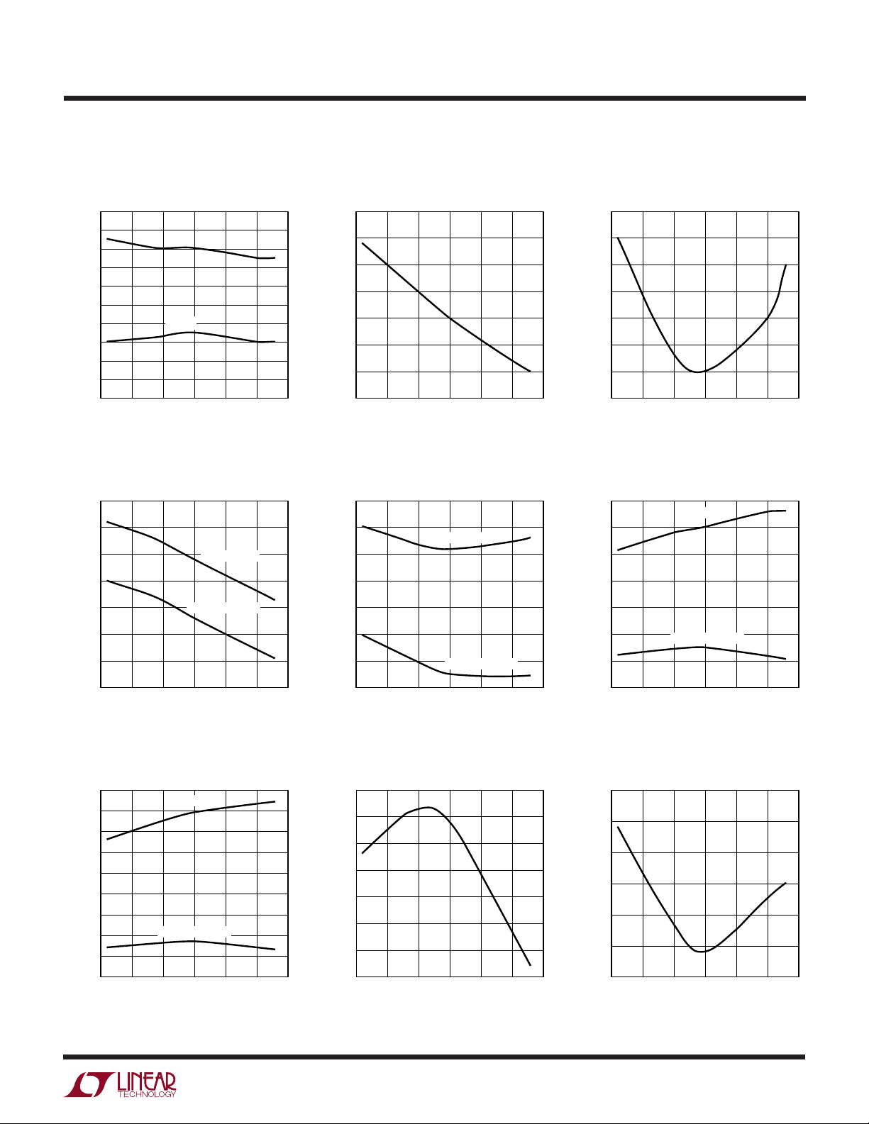
TYPICAL PERFOR A CE CHARACTERISTICS
3.3V and 5V Current Foldback
Profile
60
50
3.3V
40
30
VOLTAGE (mV)
20
10
0
0
5V
234
1
VOLTAGE (V)
12V Foldback Current Limit vs
Temperature
0.9
12V
0.8
0.7
0.6
0.5
0.4
CURRENT (A)
0.3
0.2
0.1
0
–50
= 10V
OUT
12V
= 0V
OUT
–25 0 25 7550
TEMPERATURE (°C)
4244 G01
4244 G04
100
12V
Current vs 12V
OUT
Voltage
1.0
0.9
0.8
0.7
0.6
0.5
0.4
CURRENT (A)
0.3
0.2
0.1
5
0
246 108
0
VOLTAGE (V)
VEE Foldback Current Limit vs
Temperature
0.6
0.5
0.4
0.3
CURRENT (A)
0.2
0.1
0
–50
V
EEOUT
V
EEOUT
–25 0 25 7550
TEMPERATURE (°C)
= 10V
= 0V
OUT
4244 G02
4244 G05
12
100
V
Current vs V
EEOUT
EEOUT
Voltage
12V Internal Switch Voltage Drop
vs Temperature
VEE Internal Switch Voltage Drop
vs Temperature
0.14
I
= 100mA
VEEIN
0.12
0.10
0.08
0.06
VOLTAGE (V)
0.04
0.02
4
0
–25 0 25 7550
–50
TEMPERATURE (°C)
4244 G07
100
5VIN Foldback Current Limit
Voltage vs Temperature
60
5V
= 3V
50
40
30
VOLTAGE (mV)
20
10
0
–50
–25 0 25 7550
OUT
5V
= 0V
OUT
TEMPERATURE (°C)
3.3VIN Foldback Current Limit
Voltage vs Temperature
100
4244 G08
42441f
UW
TEMPERATURE (°C)
–50
CURRENT (mA)
–25 0 25 7550
4244 G12
100
3.94
3.93
3.92
3.90
3.91
3.89
3.88
3.87
TEMPERATURE (°C)
–50
VOLTAGE (V)
–25 0 25 7550
4244 G15
100
4.34
4.32
4.30
4.26
4.28
4.24
4.22
4.20
RAMPING-UP
RAMPING-DOWN
TEMPERATURE (°C)
–50
VOLTAGE (V)
–25 0 25 7550
4244 G18
100
–11.050
–11.055
–11.060
–11.070
–11.065
–11.075
–11.080
TYPICAL PERFOR A CE CHARACTERISTICS
LTC4244/LTC4244-1
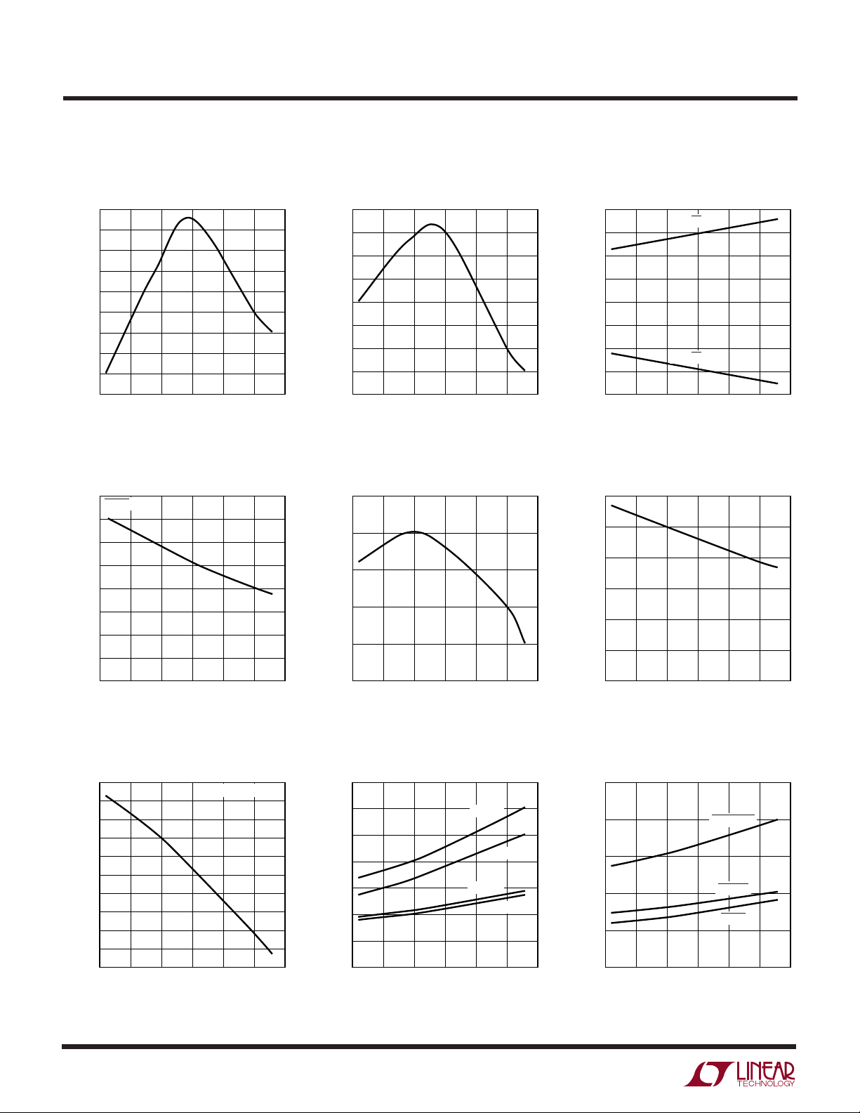
3.3VIN and 5VIN Circuit Breaker
Trip Voltage vs Temperature
52.0
51.8
51.6
51.4
51.2
51.0
50.8
VOLTAGE (mV)
50.6
50.4
50.2
50.0
–50
–25 0 25 7550
5V
IN
3.3V
IN
TEMPERATURE (°C)
12VIN Undervoltage Lockout vs
Temperature
9.30
9.25
9.20
9.15
RAMPING-UP
4244 G10
100
3.3VIN and 5VIN Circuit Breaker
Trip Filter Time vs Temperature
25.0
24.5
24.0
23.5
23.0
TIME (µs)
22.5
22.0
21.5
–25 0 25 7550
–50
V
EEIN
TEMPERATURE (°C)
Undervoltage Lockout vs
Temperature
–9.22
–9.24
–9.26
–9.28
RAMPING-UP
12VIN Supply Current vs
Temperature
100
4244 G11
5VIN Undervoltage Lockout vs
Temperature
9.10
VOLTAGE (V)
9.05
9.00
8.95
–50
–25 0 25 7550
RAMPING-DOWN
TEMPERATURE (°C)
3.3VIN Undervoltage Lockout vs
Temperature
2.54
2.53
2.52
2.51
2.50
2.49
VOLTAGE (V)
2.48
2.47
2.46
2.45
–50
RAMPING-UP
RAMPING-DOWN
–25 0 25 7550
TEMPERATURE (°C)
4244 G13
4244 G16
100
100
–9.30
VOLTAGE (V)
–9.32
–9.34
–9.36
–25 0 25 7550
–50
12V
TEMPERATURE (°C)
Powergood Threshold
OUT
Voltage vs Temperature
11.090
11.085
11.080
11.075
11.070
VOLTAGE (V)
11.065
11.060
11.055
–25 0 25 7550
–50
TEMPERATURE (°C)
RAMPING-DOWN
4244 G14
4244 G17
100
100
V
Powergood Threshold
EEIN
Voltage vs Temperature
42441f
5
LTC4244/LTC4244-1
TEMPERATURE (°C)
–50
CURRENT (µA)
–25 0 25 7550
4244 G21
100
80
60
40
0
20
–20
–40
–80
–60
OFF/ON = 0V
OFF/ON = 4V
TEMPERATURE (°C)
–50
CURRENT (mA)
–25 0 25 7550
4244 G24
100
60
50
40
20
30
10
0
UW
TYPICAL PERFOR A CE CHARACTERISTICS
5V
Powergood Threshold
OUT
Voltage vs Temperature
4.603
4.602
4.601
4.600
4.599
4.598
VOLTAGE (V)
4.597
4.596
4.595
4.594
–25 0 25 7550
–50
TEMPERATURE (°C)
100
4244 G19
3.3V
Powergood Threshold
OUT
Voltage vs Temperature
2.902
2.901
2.900
2.899
2.898
VOLTAGE (V)
2.897
2.896
2.895
2.894
–25 0 25 7550
–50
TEMPERATURE (°C)
Gate Pin Current vs Temperature
100
4244 G20
Gate Pin Fault Current vs
Temperature
16
FAULT = 0V
14
12
10
8
6
CURRENT (mA)
4
2
0
–25 0 25 7550
–50
TEMPERATURE (°C)
Timer Threshold Voltage vs
Temperature
1.66
1.64
1.62
1.60
1.58
1.56
1.54
VOLTAGE (V)
1.52
1.50
1.48
1.46
6
–25 0 25 7550
–50
TEMPERATURE (°C)
12VIN – V
4244 G22
TIMER
4244 G25
100
100
Timer Pin On Current vs
Temperature
20.30
20.25
20.20
20.15
CURRENT (µA)
20.10
20.05
–25 0 25 7550
–50
TEMPERATURE (°C)
100
4244 G23
Timer Pin Off Current vs
Temperature
Discharge Resistance vs
Temperature VOL vs Temperature
700
600
500
400
300
RESISTANCE (Ω)
200
100
0
–25 0 25 7550
–50
TEMPERATURE (°C)
12V
3.3V
OUT
OUT
V
EEOUT
5V
OUT
100
4244 G26
250
200
150
100
RESISTANCE (Ω)
50
0
–25 0 25 7550
–50
RESETOUT
PWRGD
FAULT
100
TEMPERATURE (°C)
4244 G27
42441f

LTC4244/LTC4244-1
U
UU
PI FU CTIO S
12VIN (Pin 1): 12V Supply Input. A 0.5Ω switch is con-
nected between 12VIN and 12V
limit. An undervoltage lockout circuit prevents the switches
from turning on while the 12VIN pin voltage is less than 9V.
12VIN also provides power to the LTC4244’s internal V
node.
V
(Pin 2): –12V Supply Input. A 1Ω switch is con-
EEIN
nected between V
limit. An undervoltage lockout circuit prevents the switches
from turning on while the V
–9.25V. The V
abled for the LTC4244-1.
5V
(Pin 3): 5V Output Sense. The PWRGD pin will not
OUT
pull low until the 5V
active pull-down discharges 5V
power switches are turned off.
TIMER (Pin 4): Current Fault Inhibit Timing Input and
Auxiliary VCC. Connect a capacitor from TIMER to GND.
When the LTC4244 is turned on, a 21µA pull-up current
source is connected to TIMER. Current limit faults will be
ignored until the voltage at the TIMER pin rises to within
1.6V of 12VIN. After the TIMER pin has completed ramping up, the TIMER capacitor serves as an auxiliary charge
reservoir for VCC in the event the 12VIN pin voltage
momentarily drops below the undervoltage lockout threshold voltage. When the LTC4244 is turned off (OFF/ON >
2V), the TIMER pin is pulled down to GND. After the TIMER
pin voltage drops to within 0.8V of GND, the TIMER latch
is reset and the part is ready for another power cycle.
EEIN
and V
EEIN
EEIN
undervoltage lockout function is dis-
pin voltage exceeds 4.61V. A 200Ω
OUT
with a foldback current
OUT
with a foldback current
EEOUT
pin voltage is greater than
to ground when the
OUT
CC
OFF/ON (Pin 5): Digital Input. Connect the CPCI BD_SEL#
signal to the OFF/ON pin. When the OFF/ON pin is pulled
low, the GATE pin is pulled high by a 67µ A current source
and the internal 12V and –12V switches are turned on.
When the OFF/ON pin is pulled high, the GATE pin will be
pulled to ground by a 60µ A current source and the 12V and
–12V switches turn off.
FAULT (Pin 6): Open-Drain Digital I/O. FAULT is pulled low
when a current limit fault is detected. Current limit faults
are ignored until the voltage at the TIMER pin is within 1.6V
of 12VIN. Once the TIMER cycle is complete, FAULT will
pull low and the LTC4244 latches off in the event of an
overcurrent fault. The part will remain in the latched off
state until the OFF/ON pin is cycled high then low. Forcing
the FAULT pin low with an external pull-down will cause
the part to latch into the off state after a 25µs deglitching
time.
PWRGD (Pin 7): Open-Drain Digital Power Good Output.
Connect the CPCI HEALTHY# signal to the PWRGD pin.
PWRGD remains low while V
2.9V, V
the supplies falls below its power good threshold voltage,
PWRGD will go high after a 14µs deglitching time.
GND (Pin 8): Device Ground.
RESETIN (Pin 9): Digital Input. Connect the CPCI PCI_RST#
signal to the RESETIN pin. Pulling the RESETIN pin low will
cause RESETOUT to pull low. RESETOUT will also pull low
when PWRGD is high.
≥ 4.61V, and V
5VOUT
12VOUT
EEOUT
≥ 11.1V, V
≤ –11.1V. When any of
3.3VOUT
≥
42441f
7

LTC4244/LTC4244-1
U
UU
PI FU CTIO S
RESETOUT (Pin 10): Open-Drain Digital Output. Connect
the CPCI_LOCAL_RST# signal to the RESETOUT pin.
RESETOUT is the logical combination of the RESETIN and
PWRGD.
DRIVE (Pin 11): Precharge Base Drive Output. Provides
base drive for an external NPN emitter-follower that in turn
biases the PRECHARGE node.
PRECHARGE (Pin 12): Precharge Monitor Input. An internal error amplifier servos the DRIVE pin voltage to keep the
PRECHARGE node at 1V. See Applications Information for
generating voltages other than 1V. If not used, tie the
PRECHARGE pin to ground.
5VIN (Pin 13): 5V Supply Sense Input. An undervoltage
lockout circuit prevents the switches from turning on
when the voltage at the 5VIN pin is less than 4.25V.
5V
resistor placed in the supply path between 5VIN and
5V
a constant 51mV across the sense resistor and a constant
current through the switch while the TIMER pin is low. A
foldback feature makes the current limit decrease as the
voltage at the 5V
TIMER pin is high, the circuit breaker function is enabled.
If the voltage across the sense resistor exceeds 52mV, the
circuit breaker is tripped after a 25µs time delay. In the
event of a short-circuit or large overcurrent transient
condition, the GATE pin voltage will be adjusted to maintain a constant 150mV across the sense resistor and a
constant current through the switch.
(Pin 14): 5V Current Limit Sense. With a sense
SENSE
, the GATE pin voltage will be adjusted to maintain
SENSE
pin approaches GND. When the
OUT
GATE (Pin 15): High Side Gate Drive for the External 3.3V
and 5V N-Channel Pass Transistors. An external series RC
network is required for current limit loop compensation
and setting the minimum ramp-up time. During power-up,
the slope of the voltage rise at the GATE is set by the 67µ A
current source connected through a Schottky diode to
12VIN and the external capacitor connected to GND (C1 in
Figure 1) or by the 3.3V or 5V current limit and the bulk
capacitance in the 3.3V
power down, the slew rate of the GATE voltage is set by the
60µ A current source connected to GND and the external
GATE capacitor (C1 in Figure 1).
The voltage at the GATE pin will be modulated to maintain
a constant current when either the 5V or 3.3V supplies go
into current limit. In the event of an overcurrent fault, the
GATE pin is immediately pulled to GND.
3.3V
sense resistor placed in the supply path between 3.3V
and 3.3V
maintain a constant 51mV across the sense resistor and a
constant current through the switch while the TIMER pin
is low. A foldback feature makes the current limit decrease
as the voltage at the 3.3V
the TIMER pin is high, the circuit breaker function is
enabled. If the voltage across the sense resistor exceeds
52mV, the circuit breaker is tripped after a 25µ s time delay.
In the event of a short-circuit or large overcurrent transient
condition, the GATE pin voltage will be adjusted to maintain a constant 150mV across the sense resistor and a
constant current through the switch.
(Pin 16): 3.3V Current Limit Sense. With a
SENSE
, the GATE pin voltage will be adjusted to
SENSE
or 5V
OUT
pin approaches GND. When
OUT
supply lines. During
OUT
IN
8
If no 3.3V input supply is available, short the 3.3V
to the 5VIN pin.
SENSE
pin
42441f

LTC4244/LTC4244-1
U
UU
PI FU CTIO S
3.3VIN (Pin 17): 3.3V Supply Sense Input. An undervoltage lockout circuit prevents the switches from turning on
when the voltage at the 3.3VIN pin is less than 2.5V. If no
3.3V input supply is available, short the 3.3VIN pin to the
5VIN pin.
3.3V
Output Supply Voltage. The PWRGD pin cannot pull low
until the 3.3V
supply is available, tie the 3.3V
200Ω active pull-down discharges 3.3V
when the power switches are turned off.
(Pin 18): Analog Input Used to Monitor the 3.3V
OUT
pin voltage exceeds 2.9V. If no 3.3V input
OUT
pin to the 5V
OUT
OUT
to ground
OUT
pin. A
V
connected between V
than –11.1V before the PWRGD pin pulls low. The V
power good comparator is disabled for the LTC4244-1. A
390Ω active pull-up discharges V
the power switches are turned off.
12V
connected between 12VIN and 12V
exceed 11.1V before the PWRGD pin can pull low. A 440Ω
active pull-down discharges 12V
power switches are turned off.
(Pin 19): -12V Supply Output. A 1Ω switch is
EEOUT
and V
EEIN
(Pin 20): 12V Supply Output. A 0.5Ω switch is
OUT
. V
EEOUT
EEOUT
to ground when the
OUT
must be less
EEOUT
to ground when
. 12V
OUT
OUT
EEOUT
must
42441f
9

LTC4244/LTC4244-1
W
BLOCK DIAGRA
3.3V
IN
17
3.3V
SENSE
16
GATE
15
5V
SENSE
14
5V
IN
13
–
5V
CURRENT
FAULT
UVL
MONITOR
V
EEIN
REF
8µs
RISING
EDGE
DELAY
+
50mV
+
–
TIMER_LO ≥ 50mV
TIMER_HI ≥ 150mV
5V
+
+
OUT
GND
8
V
CC
–
–
+
–
12V
IN
CP_OFF
V
67µA
60µA
CC
3.3V
OUT
–
+
+
–
+
–
TIMER_LO ≥ 50mV
TIMER_HI ≥ 150mV
50mV
+
–
3.3V
+
–
CURRENT FAULT
FAULT
6
OFF/ON
5
PWRGD
7
RESETOUT
10
RESETIN
9
CP_OFF
THERMAL FAULT
12V
IN
1
CP_OFF
V
CC
UVL
V
CC
RESET
12V SWITCH
CONTROL
CHARGE
PUMP
46µs
FALLING
EDGE
DELAY
12V CURRENT FAULT
CP_OFF
21µA
14µs
FALLING
EDGE
DELAY
REF
TIMER_HI
POWER GOOD
MONITOR
TIMER
4
3.3V CURRENT FAULT
5V CURRENT FAULT
CURRENT FAULT
V
EE
12V CURRENT FAULT
SQ
RQ
V
CC
THERMAL
SHUTDOWN
V
CC
REFERENCE
THERMAL
FAULT
TIMER_LO
THERMAL
FAULT
REF
TIMER_HI
25µs
RISING
EDGE
DELAY
5V
IN
4R
–
R
+
V
CC
SQ
R
CP_OFF
Q
DRIVE
PRECHARGE
12V
OUT
5V
OUT
3.3V
OUT
11
12
20
3
18
V
EEIN
2
THERMAL FAULT
10
CP_OFF
VEE SWITCH
CONTROL
CURRENT FAULT
V
EE
V
EEOUT
19
4244 BD
42441f

WUUU
APPLICATIO S I FOR ATIO
LTC4244/LTC4244-1
Hot Circuit Insertion
When a circuit board is inserted into a live CompactPCI
(CPCI) bus, the supply bypass capacitors can draw huge
inrush currents from the CPCI power bus as they charge
up. These transient currents can create glitches on the
power bus, causing other boards in the system to reset.
The LTC4244 is designed to turn a board’s back-end
supply voltages on and off in a controlled manner, allowing the board to be safely inserted or removed from a live
CPCI connector without glitching the system power supplies. It also protects the system supplies from shorts,
precharges the bus I/O connector pins during hot insertion
and extraction, and monitors the supply voltages.
The LTC4244 is specifically designed for CPCI applications where the Hot Swap controller resides on the plugin board.
LTC4244 Feature Summary
• Allows safe insertion and removal from a CPCI backplane.
• Controls all four CPCI supplies: -12V, 12V, 3.3V and 5V.
• Current limit during power up: the supplies are allowed
to power up in current limit. This allows the LTC4244 to
power up boards with widely varying capacitive loads
without tripping the circuit breaker. The maximum
allowable power-up time is adjustable using the TIMER
pin capacitor.
• Internal 12V and –12V power switches.
• PWRGD output: monitors the voltage status of the four
back-end supply voltages.
• PCI_RST# combined on chip with HEALTHY# to create
LOCAL_PCI_RST# output. Simply connect the
PCI_RST# signal to the RESETIN pin and the
LOCAL_PCI_RST# signal to the open-drain RESETOUT
pin.
• Precharge output: on-chip reference and error amplifier
provide 1V for biasing bus I/O connector pins during
CPCI card insertion and extraction.
• TIMER/AUX. VCC: After power-up, the TIMER pin capacitor serves as auxiliary VCC, thus enabling the
LTC4244 to ride out large voltage spikes on the 12V
supply without interruption.
IN
• Adjustable foldback current limit for the 5V and 3.3V
supplies: an adjustable analog current limit with a value
that depends on the output voltage. If the output is
shorted to ground the current limit drops to keep power
dissipation and supply glitches to a minimum.
• 12V and –12V circuit breakers: if either supply remains
in analog foldback current limit for more than 25µ s, the
circuit breakers will trip, the supplies are turned off and
the FAULT pin is pulled low.
• Adjustable 5V and 3.3V circuit breakers: if either supply
exceeds its current limit for more than 25µ s, the circuit
breaker will trip, the supplies will be turned off and the
FAULT pin is asserted low. In the event of a short circuit
on either supply, an analog current limit will prevent the
supply current from exceeding three times the circuit
breaker threshold current.
• Undervoltage lockout: All four input voltages are protected by undervoltage lockouts.
• Space saving 20-pin SSOP package.
LTC4244 vs LTC1644
The LTC4244 is pin-for-pin compatible with the LTC1644.
There are, however, some important differences between
the two parts:
• TIMER: The LTC4244’s TIMER pin threshold voltage is
1.6V below V
up, the LTC4244’s TIMER pin also doubles as auxiliary
VCC.
•V
UVL: The LTC4244 has a –9.5V UVL threshold
EEIN
protecting the V
UVL feature.
vs 1V for the LTC1644. After power-
12VIN
supply. The LTC1644 has no V
EEIN
EEIN
42441f
11

LTC4244/LTC4244-1
WUUU
APPLICATIO S I FOR ATIO
•5VIN UVL Threshold Voltage: The LTC4244’s 5VIN UVL
threshold voltage is 4.25V vs. 2.5V for the LTC1644.
•V
power good threshold voltage is –11.1V vs –10.5V for
the LTC1644.
• Absolute Maximum Ratings: The LTC4244’s absolute
maximum ratings for the 12VIN and V
±14.4V, respectively, vs ±13.2V for the LTC1644.
• 5V/3.3V Circuit Breakers: If a short-circuit occurs after
power-up, the LTC4244 actively limits the voltage
dropped across the external 5V and 3.3V sense resistors to 150mV for 25µs before tripping the circuit
breaker. In the event either the 5V or 3.3V sense resistor
voltage exceeds 150mV, the LTC1644 trips the circuit
breaker without delay.
• 5V/3.3V Circuit Breaker Threshold Voltage: The LTC4244
threshold voltage is 52mV ±5mV vs 55mV ±15mV for
the LTC1644.
• External Gate Voltage: After power-up, the voltage drop
from the 12VIN pin to the GATE pin is 0.6V for the
LTC4244 vs 50mV for the LTC1644.
Hot Plug Power-Up Sequence
The LTC4244 is specifically designed for hot plugging
CPCI boards. The typical application circuit is shown in
Figure 1.
CPCI Connector Pin Sequence
The staggered lengths of the CPCI male connector pins
ensure that all power supplies are physically connected to
the LTC4244 before back-end power is allowed to ramp up
(BD_SEL# asserted low). The long pins, which include 5V,
3.3.V, V(I/O) and GND, mate first. The short BD_SEL# pin
mates last. At least one long 5V power pin must be
connected to the LTC4244 in order for the PRECHARGE
voltage to be available during the insertion sequence.
PWRGD Threshold Voltage: The LTC4244 V
EEOUT
pins are
EEIN
EEOUT
The following is a typical hot insertion sequence:
1. ESD clips make contact.
2. Long power and ground pins make contact and Early
Power is established. The 1V precharge voltage becomes valid at this stage of insertion. Power is also
applied to the pull-up resistors connected to the FAULT,
PWRGD and OFF/ON pins. All power switches are held
off at this stage of insertion.
3. Medium length pins make contact. Both FAULT and
PWRGD continue to be pulled up high at this stage in the
hot plug sequence, and the power switches are still held
off. The 12V and –12V connector pins also make
contact at this stage. Zener clamps Z1 and Z2 plus shunt
RC snubbers R16-C5 and R15-C4 help protect the V
and 12VIN pins, respectively, from large voltage transients during hot insertion.
The signal pins also connect at this point. These include
the HEALTHY# signal (which is connected to the PWRGD
pin), the PCI_RST# signal (which is connected to the
RESETIN pin) and the I/O connector pins (which are
biased at 1V by the LTC4244’s precharge circuit).
4. Short pins make contact. The BD_SEL# signal is connected to the OFF/ON pin. If the BD_SEL# signal is
grounded on the backplane, the plug-in card power-up
cycle begins immediately. System backplanes that do
not ground the BD_SEL# signal will instead have circuitry that detects when BD_SEL# makes contact with
the plug-in board. The system logic can then control the
power up process by pulling BD_SEL# low.
Power-Up Sequence
The back-end 3.3V
lated from the 3.3VIN and 5VIN power planes by external
N-channel pass transistors Q1 and Q2, respectively. Internal pass transistors isolate the back-end 12V
V
planes.
power planes from the 12VIN and V
EEOUT
OUT
and 5V
power planes are iso-
OUT
EEIN
EEIN
and
OUT
power
12
42441f

WUUU
APPLICATIO S I FOR ATIO
LTC4244/LTC4244-1
Sense resistors R1 and R2 provide current fault detection
and R5 and C1 provide current control loop compensation
as well as ramp rate control for the GATE pin voltage.
Resistors R3 and R4 prevent high frequency oscillations
in MOSFET’s Q1 and Q2.
A power-up sequence begins when the OFF/ON pin is
pulled low (Figure 2). This enables the pass transistors to
turn on and an internal 21µ A current source is connected
to TIMER. Once the pass transistors begin to conduct
current, the supplies will start to power up. Current limit
faults are ignored while the TIMER pin voltage is ramping
up and is less than (12V
– 1.6V). When all four supply
IN
voltages are within tolerance, HEALTHY# will pull low and
LOCAL_PCI_RST# is free to follow PCI_RST#.
TIMER
10V/DIV
GATE
10V/DIV
12V
OUT
10V/DIV
5V
OUT
10V/DIV
3.3V
OUT
10V/DIV
V
EEOUT
10V/DIV
BD_SEL#
10V/DIV
HEALTHY#
10V/DIV
LCL_PCI_RST#
10V/DIV
Power-Down Sequence
When the BD_SEL# signal is pulled high, a power-down
sequence begins (Figure 3).
Internal switches are connected to each of the output
voltage supply pins to discharge the bypass capacitors to
ground. The TIMER pin is immediately pulled low. The
GATE pin is pulled down by a 60µA current source to
prevent the load currents on the 3.3V and 5V supplies from
going to zero instantaneously and glitching the power
supply voltages. When any of the output voltages dips
below its threshold, the HEALTHY# signal pulls high and
LOCAL_PCI_RST# will be asserted low.
TIMER
10V/DIV
GATE
10V/DIV
12V
OUT
10V/DIV
5V
OUT
10V/DIV
3.3V
OUT
10V/DIV
V
EEOUT
10V/DIV
BD_SEL#
10V/DIV
HEALTHY#
10V/DIV
LCL_PCI_RST#
10V/DIV
10ms/DIV
Figure 2. Normal Power-Up Sequence
4244 F02
20ms/DIV
Figure 3. Normal Power-Down Sequence
4244 F03
42441f
13

LTC4244/LTC4244-1
WUUU
APPLICATIO S I FOR ATIO
Once the power-down sequence is complete, the CPCI
card may be removed from the slot. During extraction, the
precharge circuit continues to bias the bus I/O connector
pins at 1V until the long 5V and 3.3V connector pin
connections are broken.
GATE Pin Capacitor Selection
Both the load capacitance and the LTC4244’s GATE pin
capacitor (C1 in Figure 1) affect the ramp rate of the 5V
and 3.3V
voltages. The precise relationship can be
OUT
OUT
expressed as:
dV
OUT
dt
I
GATE
=
C
1
I
LIMIT(3.3V)
=
I
LIMIT(5V)
or =
I
–
LOAD V
C
LOAD VOUT
33
(. )
C
I
–
LOAD V
LOAD VOUT
5
()
33
(. )
5
()
or
(1)
whichever is slowest. The power-up time for any of the
LTC4244’s outputs where the inrush current is constrained
by that supply’s foldback current limit can be approximated as:
t
on VOUT
()
n
Where nV
<
OUT
example, if C
I
LOAD(5VOUT)
= 5A, the 5V
••
LOAD OUT
II
LIMIT VOUT LOAD VOUT
() ()
nn
= 5V
LOAD
, 3.3V
OUT
=2000µF, I
OUT
n
–
, 12V
OUT
LIMIT(5VOUT)
OUT
or V
= 6A and
EEOUT
(2)
. For
turn-on time will be less than
CV
2
20ms.
If the value of C1 is large enough that it alone determines
the output voltage ramp rate, then the magnitude of the
inrush current initially charging the load capacitance is:
C
I
INRUSH
LOAD
=
I
•
C
GATE
1
(3)
The maximum power-up time for this condition can be
approximated by:
V V C MAX
()
t
<
ON
where V
+
OUT TH MOSFET MAX
TH,MOSFET(MAX)
,()
I
GATE MIN
()
is the maximum threshold voltage
•( )1
(4)
of the external 5V or 3.3V MOSFET.
In general, the edge rate (dI/dt) at which the back-end 5V
and 3.3V supply currents are turned on can be limited by
increasing the size of C1. Applications that are sensitive to
the edge rate should characterize how varying the size of
C1 reduces dI/dt for the external MOSFET selected for a
particular design.
In the event of a short-circuit or overcurrent condition, the
LTC4244’s GATE pin can be pulled down within 2µ s since
a 1kΩ (R5 in Figure 1) decouples C1 from the gates of the
external MOSFET’s (Q1 and Q2 in Figure 1).
TIMER Pin Capacitor Selection
During a power-up sequence, a 21µA current source is
connected to the TIMER pin and current limit faults are
ignored until the voltage ramps to within 1.6V of 12VIN.
This feature allows the part to power up large capacitive
loads using its foldback current limit. The TIMER inhibit
period can be expressed as:
t
TIMER
CVV
=
•–12
TIMER IN TIMER
()
I
TIMER
(5)
The timer period should be set longer than the duration of
any inrush current that exceeds the LTC4244’s foldback
current limit but yet be short enough not to exceed the
maximum, safe operating area of the external 5V and 3.3V
pass transistors in the event of a short circuit (see Design
Example). As a design aid, the TIMER period as a function
of the timing capacitor using standard values from 0.1µ F
to 0.82µF is shown in Table 1.
14
42441f

WUUU
APPLICATIO S I FOR ATIO
LTC4244/LTC4244-1
Table 1. t
C
TIMER
vs C
TIMER
(±10%) t
0.1µF 35ms 74ms
0.22µF 77ms 162ms
0.33µF 115ms 243ms
0.47µF 164ms 346ms
0.68µF 238ms 500ms
0.82µF 287ms 603ms
TIMER
TIMER(MIN)
t
TIMER(MAX)
The TIMER pin is immediately pulled low when the BD_SEL#
pin signal goes high.
Thermal Shutdown
The internal switches for the 12V and –12V supplies are
protected by a thermal shutdown circuit. When the junction temperature of the die reaches 150°C, all switches will
be latched off and the FAULT pin will be pulled low.
TIMER
10V/DIV
Short-Circuit Protection
During a normal power-up sequence, if the TIMER pin is
done ramping and any supply is still in current limit all of
the pass transistors will be immediately turned off and
FAULT will be pulled low as shown in Figure 4.
In order to prevent excessive power dissipation in the pass
transistors and prevent voltage spikes on the supplies
during short-circuit conditions, the current limit on each
supply is designed to be a function of the output voltage.
As the output voltage drops, the current limit decreases.
Unlike a traditional circuit breaker function where large
currents can flow before the breaker trips, the current
foldback feature guarantees that the supply current will be
kept at a safe level.
If either the 12V or –12V supply exceeds current limit
after power-up, the shorted supply’s current will drop
GATE
10V/DIV
3.3V
OUT
10V/DIV
BD_SEL#
10V/DIV
HEALTHY#
10V/DIV
LCL_PCI_RST#
10V/DIV
FAULT
10V/DIV
12V
OUT
5V
OUT
10V/DIV
10V/DIV
V
EEOUT
10V/DIV
20ms/DIV
4244 F04
Figure 4. Power-Up Into a Short on a 3.3V Output
42441f
15

LTC4244/LTC4244-1
WUUU
APPLICATIO S I FOR ATIO
immediately to its I
value. If that supply remains in
LIMIT
current limit for more than 25µ s, all of the supplies will be
latched off. The 25µ s prevents quick current spikes—for
example, from a fan turning on—from causing false trips
of the circuit breaker.
After power-up, the 5V and 3.3V supplies are protected
from short circuits by dual-level circuit breakers. In the
event that either supply’s current exceeds the nominal
current limit, an internal timer is started. If the supply is
still overcurrent after 25µ s, the circuit breaker trips and all
the supplies are turned off (Figure 5). An analog current
limit loop prevents the supply current from exceeding 3×
the nominal current limit in the event of a short circuit
(Figure 6). The LTC4244 will stay in the latched off state
until the OFF/ON pin is cycled high then low or the 12V
IN
power supply is cycled low then high.
The current limit and the foldback current level for the 5V
and 3.3V outputs are both a function of the external sense
resistor. As shown in Figure 1, a sense resistor is connected between 5VIN and 5V
for the 5V supply. For
SENSE
the 3.3V supply, a sense resistor is connected between
3.3VIN and 3.3V
. The typical current limit and the
SENSE
foldback current levels are given by Equations 6 and 7:
mV
I
LIMIT VOUT
()
n
I
FOLDBACK VOUT
where nV
OUT
()
n
= 5V
51
=
R
SENSE VOUT
=
R
or 3.3V
OUT
()
n
mV
16
SENSE VOUT
()
n
.
OUT
(6)
(7)
The current limit for the internal 12V switch is set at
850mA folding back to 360mA and the –12V switch at
610mA folding back to 225mA.
5V
IN
100mV/DIV
20V/DIV
10V/DIV
20V/DIV
– 5V
GATE
5V
OUT
FAULT
5V/DIV
TIMER
SENSE
10µs/DIV
Figure 5. Overcurrent Fault on 5V Output
4244 F05
3V
IN
500mV/DIV
GATE
20V/DIV
3.3V
OUT
5V/DIV
FAULT
5V/DIV
TIMER
20V/DIV
– 3V
SENSE
10µs/DIV
Figure 6. Short-Circuit Fault on 3.3V Output
4244 F06
16
42441f

WUUU
APPLICATIO S I FOR ATIO
LTC4244/LTC4244-1
Calculating R
SENSE
Determining the most appropriate value for the sense
resistor first requires knowing the maximum current needed
by the load under worst-case conditions. Two other parameters affect the value of the sense resistor. First is the
tolerance of the LTC4244’s circuit breaker threshold voltage. The LTC4244’s nominal circuit breaker threshold
voltage is V
CB(NOM)
= 52mV; however it exhibits ±5mV
tolerance over process and temperature. Second is the
tolerance (RTOL) of the sense resistor. Sense resistors are
available in RTOL’s of ±1%, ±2% and ±5% and exhibit
temperature coefficients of resistance (TCR’s) between
±75ppm/°C and ±100ppm/°C. How the sense resistor
changes as a function of temperature depends on the
I2 • R power being dissipated by it. The power rating of the
sense resistor should accommodate steady-state fault
current levels so that the component is not damaged
before the circuit breaker trips.
Table 2 lists I
TRIP(MIN)
gested values of R
and I
TRIP(MAX)
. Table 7 lists manufacturers and
SENSE
versus some sug-
part numbers for these resistor values.
Table 2. I
R
SENSE
vs R
TRIP
(1% RTOL) I
0.005Ω 9.31A 11.5A
0.007Ω 6.6A 8.2A
0.011Ω 4.2A 5.2A
SENSE
TRIP(MIN)
I
TRIP(MAX)
Output Voltage Monitor
The status of all four output voltages is monitored by the
power good function. In addition, the PCI_RST# signal is
logically combined on-chip with the HEALTHY# signal to
create LOCAL_PCI_RST# (see Table 3). As a result,
LOCAL_PCI_RST# will be pulled low whenever HEALTHY#
is pulled high independent of the state of the PCI_RST#
signal.
If any of the output voltages drop below the power good
threshold for more than 14µs, the PWRGD pin will be
pulled high and the LOCAL_PCI_RST# signal will be
asserted low.
Table 3. LOCAL_PCI_RST# Truth Table
PCI_RST# HEALTHY# LOCAL_PCI_RST#
LO LO LO
LO HI LO
HI LO HI
HI HI LO
Precharge
The PRECHARGE input and DRIVE output pins are intended for use in generating the 1V precharge voltage that
is used to bias the bus I/O connector pins during board
insertion and extraction. The LTC4244 is also capable of
generating precharge voltages other than 1V. Figure 7
shows a circuit that can be used in applications requiring
a precharge voltage of less than 1V. The circuit in Figure␣ 8
can be used for applications that need precharge voltages
greater than 1V.
Precharge resistors are used to connect the 1V bias voltage to the I/O lines with minimal disturbance. Figure 1
shows the precharge application circuit for 5V signaling.
The precharge resistor requirements are more stringent
for 3.3V and Universal Hot Swap boards. If the total leakage current on the I/O line is less 2µ A, then a 50k resistor
can be connected directly from the 1V bias voltage to the
I/O line. However, many ICs connected to the I/O lines can
have leakage currents up to 10µ A. For these applications,
a 10k resistor is used but must be disconnected when the
board is seated as determined by the state of the BD_SEL#
signal. Figure 9 shows a precharge circuit that uses a bus
switch to connect the individual 10k precharge resistors to
the LTC4244’s 1V PRECHARGE pin. The electrical connection is made (bus switches closed) when the voltage on the
BD_SEL# pin of the plug-in card is pulled-up to 5VIN,
which occurs just after the long pins have made contact.
The bus switches are electrically disconnected when the
short, BD_SEL# connector pin makes contact and the
42441f
17

LTC4244/LTC4244-1
WUUU
APPLICATIO S I FOR ATIO
LTC4244*
128
R10A
DRIVEPRECHARGE
11
Q3
MMBT2222A
• 1V
1k
5%
12Ω
5%
3.3V
GND
18Ω
4.7nF
5%
R10BR10A
PRECHARGE OUT
V
PRECHARGE
*ADDITIONAL DETAILS OMITTED FOR CLARITY
=
R10A + R10B
Figure 7. Precharge Voltage <1V Application Circuit
5V
LONG 5V
BD_SEL#
GROUND
I/O PIN 1
• • •
I/O PIN 128
BACKPLANE
CONNECTOR
PCB EDGE
BACKPLANE
CONNECTOR
Z4: SMAJ5.0A
*ADDITIONAL DETAILS OMITTED FOR CLARITY
R22
2.7Ω
C7
0.01µF
DATA BUS
C9
0.01µF PER
POWER PIN
Z4
5V
IN
4244 F07
IN
R23
51.1k 5%
R20
1.2k
5%
R24
75k
5%
R19
1k 5%
100Ω
Q2
MMBT3906
LTC4244*
18Ω
5%
R10A
DRIVEPRECHARGE
11
Q3
MMBT2222A
• 1V
1k
5%
12Ω
5%
GND
128
4.7nF
R10BR10A
PRECHARGE OUT
V
PRECHARGE
*ADDITIONAL DETAILS OMITTED FOR CLARITY
R10A + R10B
=
Figure 8. Precharge Voltage >1V Application Circuit
13
5V
IN
LTC4244*
5
OFF/ON
GND
PRECHARGE DRIVE
• • •
R8
1k 5%
R7
12Ω 5%
I/O
I/O
0.1µF
R13
10Ω
5%
R14
10Ω
5%
8
R10
18Ω 5%
12 11
R9
24Ω
IN
V
DD
BUS SWITCH
OE
OUT OUT
R11
R12
10k
10k
5%
5%
• • •
UP TO 128 I/O LINES
C3 4.7nF
MMBT2222A
PRECHARGE OUT
I
OUT
Q3
1V ±10%
= ±55mA
3.3V
4244 F08
PCI
BRIDGE
CHIP
IN
3V
4244 F09
IN
18
Figure 9. Precharge Bus Switch Application Circuit for 3.3V and Universal Hot Swap Boards
42441f

WUUU
APPLICATIO S I FOR ATIO
LTC4244/LTC4244-1
BD_SEL# voltage drops below 4.4V thus causing the bus
switch OE to be pulled high by Q2.
The CompactPCI specification assumes that there is a
diode to 3.3V on the circuit that is driving the BD_SEL# pin.
The 1.2k resistor pull-up to 5VIN on the plug-in card will be
clamped by the diode to 3.3V. If the BD_SEL# pin is being
driven high, the actual voltage on the pin will be approximately 3.9V. This is still above the high TTL threshold of
the LTC4244 OFF/ON pin, but low enough for Q2 to disable
the bus switches and thus disconnect the 10k precharge
resistors from the I/O lines. Since the power to the bus
switch is derived from a front-end power plane, a 100Ω
resistor should be placed in series with the power supply
of the bus switch.
When the plug-in card is removed from the connector, the
BD_SEL# connection is broken first, and the BD_SEL#
voltage pulls up to 5VIN. This causes Q2 to turn off, which
re-enables the bus switch, and the precharge resistors are
again connected to the LTC4244 PRECHARGE pin for the
remainder of the extraction process.
TIMER/Auxiliary V
CC
Once the TIMER pin voltage has ramped to within 1.6V of
12VIN, the auxiliary VCC function is enabled. In the event
the 12VIN supply voltage collapses, the LTC4244 will
continue to draw power from the charge stored on the
TIMER pin capacitor until the internal VCC node drops
below its undervoltage lockout threshold or the 12V
IN
supply voltage recovers, whichever happens first.
Other CompactPCI Applications
The LTC4244-1 is designed for CompactPCI designs
where the –12V supply is not being used on the plug-in
board. The V
and VEE circuit breaker functions are disabled. The V
pin should be connected to GND and the V
power good comparator, V
EEOUT
EEIN
EEOUT
UVL,
EEIN
pin left
floating if a –12V output is not needed.
If no 3.3V supply input is required, Figure 10 illustrates
how the LTC4244 should be configured: 3.3V
3.3VIN are connected to 5VIN and 3.3V
5V
.
OUT
is connected to
OUT
SENSE
and
For applications where the BD_SEL# connector pin is
typically connected to ground on the backplane, the circuit
in Figure 11 allows the LTC4244 to be reset simply by
pressing a pushbutton switch on the CPCI plug in board.
This arrangement eliminates the requirement to extract
and reinsert the CPCI board in order to reset the LTC4244’s
circuit breaker.
V(I/O)
PCB EDGE
BACKPLANE
CONNECTOR
BD_SEL#
GROUND
*ADDITIONAL PINS OMITTED FOR CLARITY
Figure 11. BD_SEL# Pushbutton Toggle Switch
BACKPLANE
CONNECTOR
PUSHBUTTON
SWITICH
100Ω
0.25W
1.2k
1k
5
8
OFF/ON
LTC4244*
GND
4244 F11
5V
LONG 5V
GROUND
BACKPLANE
CONNECTOR
Z4: SMAJ5.0A
*ADDITIONAL PINS OMITTED FOR CLARITY
PCB EDGE
BACKPLANE
CONNECTOR
5V
IN
Z4
3.3V
8
GND
Figure 10. No 3.3V Supply Application Circuit
R2
0.007Ω
1317 16 18 31514
3.3V
IN
SENSE
5V
5V
IN
LTC4244*
SENSE
Q2
IRF7457
GATE
R4
10Ω
3.3V
OUT
5V
OUT
C1
R5
0.33µF
1k
5V
OUT
4244 F10
42441f
19

LTC4244/LTC4244-1
WUUU
APPLICATIO S I FOR ATIO
Power MOSFET Selection Criteria
The LTC4244 uses external MOSFETs to limit the 5V and
3.3V supply currents. The following criteria should be
used when selecting these MOSFET’s:
1. The on resistance should be low enough to prevent an
excessive voltage drop across the sense resistor and
the series MOSFET at rated load current given the
amount of gate to source voltage provided by the
LTC4244.
2. The drain-to-source breakdown voltage should be high
enough for the device to survive overvoltage transients
that may occur during fault conditions (the 5V and 3.3V
transient voltage limiters shown in Figure 1 will limit the
maximum drain-source voltage seen by these MOSFET’s
during fault conditions).
3. The MOSFET package must be able to handle the
maximum, steady state power dissipation for the ON
state without exceeding the device’s rated maximum
junction temperature. The MOSFET’s steady-state, dissipated power can be expressed as:
PON = I
MAX
2
• R
DS(ON)
(8)
The increase in steady-state junction-to-ambient temperature is given by:
TJ – TA = PON • R
θJA
(9)
4. The MOSFET package must be able to dissipate the heat
resulting from the power pulse during the transition
from off to on. A worst-case approximation for the
magnitude of the power pulse is:
P
OFF-ON
where nV
VI I
n
<
= 5V
OUT
•
()
OUT INRUSH LOAD
or 3.3V
OUT
+
2
, I
OUT
INRUSH
(10)
is the transient current initially charging the load capacitance and
I
is the steady-state load current. The duration, tON,
LOAD
of the power pulse can be expressed as:
CV
t
=
ON
•
LOAD OUT
I
INRUSH
(11)
5. The MOSFET package must be able to sustain the
maximum pulse power that occurs in the event the
LTC4244 attempts to power-up either the 5V or 3.3V
back-end supply into a short circuit (see Design Example for a sample calculation).
Table 8 lists some power MOSFET’s that can be used with
the LTC4244.
Input Overvoltage Transient Protection
Hot plugging a board into a backplane generates inrush
currents from the backplane power supplies due to the
charging of the plug-in board capacitance. To reduce this
transient current to a safe level, the CPCI Hot Swap
specification restricts the amount of unswitched capacitance used on the input side of the plug-in board. Each
medium or long power pin connected to the CPCI female
connector on the plug-in board is required to have a 10nF
ceramic bypass capacitor to ground. Bulk capacitors are
only allowed on the switched output side of the LTC4244
(5V
OUT
, 3.3V
OUT
, 12V
OUT
, V
). Some bulk capaci-
EEOUT
tance is allowed on the 5VIN and 3.3VIN Early Power
planes, but only because a current limiting resistor is
assumed to decouple the connector pin from the bulk
capacitance. Circuits normally placed on the unswitched
side Early Power plane (PCI Bridge, for example) need to
to be decoupled by a current limiting resistor.
Disallowing bulk capacitors on the input power pins mitigates the inrush current during Hot Swap. However, it also
tends to create a resonant circuit formed by the inductance
of the backplane power supply trace in series with the
inductance of the connector pin and the parasitic capacitance of the plug-in board (mainly due to the large power
FET). Upon board insertion, the ringing of this circuit can
exhibit a peak overshoot of 2.5 times the steady-state
voltage (>30V for 12VIN).
There are two methods for abating the effects of these high
voltage transients: using voltage limiters to clip the transient to a safe level and snubber networks. Snubber
networks are series RC networks whose time constants
20
42441f

WUUU
APPLICATIO S I FOR ATIO
LTC4244/LTC4244-1
are experimentally determined based on the board’s parasitic resonance circuits. As a starting point, the capacitors
in these networks are chosen to be 10× to 100× the power
MOSFET’s C
under bias. The series resistor is a value
OSS
determined experimentally that ranges from 1Ω to 50Ω,
depending on the parasitic resonance circuit. Note that in
all LTC4244 circuit schematics,
both
transient voltage
limiters and snubber networks have been added to the
12VIN and V
supply rails and should always be used.
EEIN
Snubber networks are not necessary on the 3.3VIN or the
5V
IN
5V
3V
IN
3.3V
Z3 Z4
3.3V
0.005Ω
17
IN
R1
3.3V
SENSE
Q1
IRF7457
15
GATE
R3
10Ω
3.3V
LTC4244*
18
OUT
GND
5VIN supply lines since their absolute maximum voltage
ratings are 13.5V. Transient voltage limiters, however, are
recommended as these devices provide large-scale transient protection for the LTC4244 in the event of abrupt
changes in supply current. All protection networks should
be mounted very close to the LTC4244’s supply pins using
short lead lengths to minimize trace resistance and inductance. This is shown schematically in Figures 12 and 13
and a recommended layout of the transient protection
devices around the LTC4244 is shown in Figure 14.
R2
0.007Ω
13
5V
IN
5V
1416
SENSE
Q2
IRF7457
R4
10Ω
5V
OUT
5V
3V
OUT
3.3V
C1
R5
0.047µF
1k
3
5V
OUT
Z3, Z4: SMAJ5.0A
*ADDITIONAL DETAILS OMITTED FOR CLARITY
Figure 12. Place Transient Protection Devices Close to LTC4244’s 5VIN and 3.3VIN Pins
12VIN–12V
R13
Z1 Z2
10Ω
C4
0.1µF
Z1, Z2: SMAJ12CA
*ADDITIONAL DETAILS OMITTED FOR CLARITY
12V
LTC4244*
1
IN
GND
IN
2
V
EEIN
8
R14
10Ω
C5
0.1µF
4244 F16
Figure 13. Place Transient Protection Devices
Close to LTC4244’s 12VIN and V
EEIN
Pins
8
VIAS TO
GND PLANE
Z3
Z1
C5
R14
C4
R13
Z1
12V
*ADDITIONAL DETAILS OMITTED FOR CLARITY
DRAWING IS NOT TO SCALE!
IN
4244 F12
3.3V
IN
20
19
18
17
16
LTC4244*
1
2
3
4
5
V
EEIN
5V
15
14
6
7
GND
Figure 14. Recommended Layout for Transient Protection
Components
IN
13
12
11
Z4
8
9
10
4244 F14
42441f
21

LTC4244/LTC4244-1
WUUU
APPLICATIO S I FOR ATIO
PCB Layout Considerations
For proper operation of the LTC4244’s circuit breaker,
4-wire Kelvin sense connections between the sense resistor and the LTC4244’s 5VIN and 5V
and 3.3V
pins are strongly recommended. The PCB
SENSE
pins and 3.3V
SENSE
IN
layout should be balanced and symmetrical to minimize
wiring errors. In addition, the PCB layout for the sense
resistors and the power MOSFETs should include good
thermal management techniques for optimal device power
dissipation. A recommended PCB layout for the sense
resistor, the power MOSFET and the GATE drive components around the LTC4244 is illustrated in Figure 15. In Hot
CURRENT FLOW
3.3V
3.3V
TO LOAD
IN
SENSE
RESISTOR
Swap applications where load currents can be 10A, narrow PCB tracks exhibit more resistance than wider tracks
and operate at more elevated temperatures. Since the
sheet resistance of 1 ounce copper foil is approximately
0.45mΩ/o, track resistance and voltage drops add up
quickly in high current applications. Thus, to keep PCB
track resistance, voltage drop and temperature to a minimum, the suggested trace width in these applications for
1 ounce copper foil is 0.03” for each ampere of DC current.
In the majority of applications, it will be necessary to use
plated-through vias to make circuit connections from
component layers to power and ground layers internal to
CURRENT FLOW
SO-8
D
D
D
D
TO LOAD
G
S
S
S
WW
3.3V
3.3V
OUT
TRACK WIDTH W:
0.03" PER AMPERE
ON 1 OZ Cu FOIL
20
19
18
17
16
LTC4244*
1
2
3
4
5
C
TIMER
W
*ADDITIONAL DETAILS OMITTED FOR CLARITY
DRAWING IS NOT TO SCALE!
GATE
15
14
6
7
R3
R5
13
12
11
8
9
10
CURRENT FLOW
TO SOURCE
C1
VIA/PATH
TO GND
VIA TO
GND PLANE
GNDGND
4244 F15
Figure 15. Recommended Layout for Power MOSFET, Sense Resistor and GATE Components for the 3.3V Rail
22
42441f

WUUU
APPLICATIO S I FOR ATIO
LTC4244/LTC4244-1
the PC board. For 1 ounce copper foil plating, a general rule
is 1 ampere of DC current per via making sure the via is
properly dimensioned so that solder completely fills the
void. For other plating thicknesses, check with your PCB
fabrication facility.
Design Example
As a design example, consider a CPCI Hot Swap application with the following power supply requirements:
Table 4. Design Example Power Supply Requirements
VOLTAGE MAXIMUM DC LOAD
SUPPLY SUPPLY CURRENT CAPACITANCE
12V 450mA 100µF
5V 5A 2200µF
3.3V 7A 2200µF
–12V 100mA 100µF
The first step is to select the appropriate values of R
SENSE
for the 5V and 3.3V supplies. Calculating the value of
R
is based on I
SENSE
LOAD(MAX)
and the lower limit for the
circuit breaker threshold voltage (47mV for both the 5V
and 3.3V circuit breakers). If a 1% tolerance is assumed
for the sense resistors, then 5mΩ and 7mΩ resistor
values yield the following minimum and maximum I
TRIP
values:
perature curve, the device’s on-resistance can be expected
to increase by about 20% over its room temperature value.
Recalculation of the steady-state values of RON and junction temperature yields approximately 12.6mΩ and 81°C,
respectively. The I • R drop across the 3.3V sense resistor
and series MOSFET at maximum load current under these
conditions will be less than 124mV.
The next step is to select appropriate values for C1 and
C
. Assuming that the total current for the 5V supply
TIMER
is constrained to less than 6A during power-up (6 × 5V
medium length connector pins at 1A per pin), then the
inrush current shouldn’t exceed:
I
INRUSH
< 6A – I
LOAD(5VOUT)
= 6A – 5A = 1A (12)
This yields:
IF
GATE MAX
>
C
1
⇒>
1
C
()
I
INRUSH MAX
µµ
100 2200
AF
•
()
•
1
A
2200
µ
=
220
nF
(13)
Hence a C1 value of 330nF ±10% should suffice. The value
of C
for this design example will be constrained by
TIMER
the duration of the 12V supply inrush current, which
according to Equation 2 is:
Table 5. I
R
SENSE
vs R
TRIP
(1% RTOL) I
5mΩ 9.3A 11.5A
7mΩ 6.6A 8.2A
SENSE
TRIP(MIN)
I
TRIP(MAX)
So sense resistor values of 7mΩ and 5mΩ should suffice
for the 5V and 3.3V supplies, respectively.
The second step is to select MOSFETs for the 5V and 3.3V
supplies. The IRF7457’s on resistance is less than 10.5mΩ
for V
> 4.5V and a junction temperature of 25°C. Since
GS
the maximum load current requirement for the 3.3V supply is 7A, the steady-state power the device may be
required to dissipate is 514mW. The IRF7457 has a
junction-to-ambient thermal resistance of 50°C/Watt. If a
maximum ambient temperature of 50°C is assumed, this
yields a junction temperature of 75.7°C. According to the
IRF7457’s Normalized On-Resistance vs Junction Tem-
CV
••
212
t
()
ON VOUT
12
t
⇒<
()
ON VOUT
12
<
II
LIMIT MIN LOAD MAX
2 100 12
550 450
LOAD
–
() ( )
••
FV
µ
mA mA
–
=
24
(14)
ms
In order to guarantee that the LTC4244’s TIMER fault
inhibit period is greater than 24ms, the value of C
TIMER
should be:
ms I
24
•
TIMER MAX
C
C
⇒>
TIMER
TIMER
>
VV
12
–
ms A
24 26
VV
12 1 9
–.
•
()
TIMER MAX
()
µ
=
61 8
.
(15)
nF
So a value of 82nF (±10%) should suffice.
42441f
23

LTC4244/LTC4244-1
WUUU
APPLICATIO S I FOR ATIO
The next step is to verify that the thermal ratings of the
external 5V and 3.3V MOSFETs aren’t being exceeded
during power-up cycles into the designed loads or into a
short circuit.
The amount of heating in the 5V and 3.3V MOSFETs during
a normal power cycle depends on the LTC4244’s GATE pin
current (refer to Gate Current vs Temperature plot in the
Typical Performance Characteristics section). The magnitude of the off-on power pulse that results in maximum
heating of the MOSFETs is given by Equation 10 as:
P
OFF-ON
n
=
•
VI I
()
OUT INRUSH MIN LOAD VOUT
+
() ( )
n
2
(16)
where
C
I
INRUSH MIN
LOAD
C MAX
()
1
I
•=
GATE MIN() ()
(17)
The duration of the power-pulse is given by Equation 11
as:
The duration and magnitude of the power pulse that
results during a short-circuit condition on either the 5V or
3.3V outputs are a function of the TIMER capacitor and the
LTC4244’s foldback current limit. Figure 16 shows the
worst-case power dissipated in the 5V and 3.3V external
FETs vs V
5VOUT
and V
3.3VOUT
, respectively. In the case of
the 3.3V external MOSFET, the maximum dissipated power
is 24 Watts (V
3.3VOUT
the maximum dissipated power is 22 Watts (V
= 0.9V). For the 5V external MOSFET,
=
5VOUT
1.75V). The maximum duration of the short-circuit powerpulse is given by Equation 19 as:
12
VV
–
TIMER MIN
tC
t
⇒<
tms
⇒<
<
PULSE TIMER MAX
()()
PULSE
PULSE
60 3
()
82 8 2 12 1 3
nF nF V V
+
.
.• –.
•
I
TIMER MIN
16
A
µ
()
()
(19)
t
INRUSH
CV
<
•
LOAD OUT
I
n
INRUSH MIN
()
(18)
Solving these equations for the 5V and 3.3V supplies
yields:
Table 6
P
OFF-ON
5V MOSFET 12.8W 90ms
3.3V MOSFET 11.8W 60ms
t
INRUSH(MAX)
Under these conditions, the IRF7457 datasheet’s Thermal
Response vs Pulse Duration curve indicates that the
junction-to-ambient temperature will increase by 60°C for
the 5V MOSFET and 46°C for the 3.3V MOSFET.
25
20
15
10
DISSIPATED POWER (W)
5
0
0
Figure 16. Worst-Case 5V and 3.3V MOSFET
Dissipated Power vs Output Voltage
3.3V MOSFET
1
OUTPUT VOLTAGE (V)
5V R
3.3V R
2
SENSE
SENSE
5V MOSFET
3
= 0.007Ω
= 0.005Ω
4
5
4244 F16
24
42441f

WUUU
APPLICATIO S I FOR ATIO
LTC4244/LTC4244-1
The IRF7457’s Thermal Response vs Pulse Duration curve
indicates that the worst-case increase in junction-toambient temperature during a power-cycle for the 3.3V
MOSFET is less than 96°C while the worst-case increase
in junction-to-ambient temperature for the 5V MOSFET is
less than 88°C.
Power MOSFET and Sense Resistor Selection
Tables 7 and 8 list current sense resistors and power
MOSFET transistors, respectively, that can be used with
the LTC4244’s circuit breakers. Table 9 lists supplier web
site addresses for discrete components mentioned
throughout the LTC4244 data sheet.
Obtaining Information on Specific Parts
For more information or to request a copy of the
CompactPCI specification, contact the PCI Industrial Computer Manufacturers Group at:
PCI Industrial Computer Manufacturers Group
Wakefield, MA 01880 USA
Phone: 01 (718) 224-1239
Web Site: http://www.picmg.com
Transient Voltage Suppressors SMAJ12A and SMAJ5.0A
are supplied by:
Diodes, Incorporated
Westlake Village, CA 91362 USA
Phone: 01 (805) 446-4800
Web Site: http://www.vishay.com or
http://www.diodes.com
Transistors MMBT2222A and MMBT3906 are supplied
by:
ON Semiconductor
Phoenix, AZ 85008 USA
Phone: 01 (602) 244-6600
Web Site: http://www.onsemi.com
42441f
25

LTC4244/LTC4244-1
WUUU
APPLICATIO S I FOR ATIO
Table 7. Sense Resistor Selection Guide
CURRENT LIMIT VALUE PART NUMBER DESCRIPTION MANUFACTURER
1A LR120601R055F 0.055Ω, 0.5W, 1% Resistor IRC-TT
WSL1206R055 Vishay Dale
2A LR120601R028F 0.028Ω, 0.5W, 1% Resistor IRC-TT
WSL1206R028 Vishay Dale
5A LR120601R011F 0.011Ω, 0.5W, 1% Resistor IRC-TT
WSL2010R011 Vishay Dale
7.6A WSL2512R007 0.007Ω, 1W, 1% Resistor Vishay Dale
10A WSL2512R005 0.005Ω, 1W, 1% Resistor Vishay Dale
Table 8. N-Channel Power MOSFET Selection Guide
CURRENT LIMIT VALUE PART NUMBER DESCRIPTION MANUFACTURER
0A to 2A MMDF3N02HD Dual N-Channel SO-8, R
2A to 5A MMSF5N02HD Single N-Channel SO-8, R
5A to 10A MTB50N06V Single N-Channel DD-Pak, R
5A to 10A IRF7457 Single N-Channel SO-8, R
5A to 10A Si7880DP Single N-Channel PowerPAKTM, R
PowerPAK is a trademark of Vishay Siliconix
= 0.1Ω ON Semiconductor
DS(ON)
= 0.025Ω ON Semiconductor
DS(ON)
= 0.028Ω ON Semiconductor
DS(ON)
= 0.007Ω International Rectifier
DS(ON)
= 0.003 Ω Vishay Siliconix
DS(ON)
Table 9. Manufacturers’ Web Site
MANUFACTURER WEB SITE
International Rectifier www.irf.com
ON Semiconductor www.onsemi.com
IRC-TT www.irctt.com
Vishay Dale www.vishay.com
Vishay Siliconix www.vishay.com
Diodes, Inc. www.diodes.com
26
42441f

PACKAGE DESCRIPTIO
U
GN Package
20-Lead Plastic SSOP (Narrow .150 Inch)
(Reference LTC DWG # 05-08-1641)
.045 ±.005
LTC4244/LTC4244-1
.337 – .344*
(8.560 – 8.738)
1617181920
15
141312 11
.058
(1.473)
REF
.254 MIN
RECOMMENDED SOLDER PAD LAYOUT
.0075 – .0098
(0.19 – 0.25)
.016 – .050
(0.406 – 1.270)
NOTE:
1. CONTROLLING DIMENSION: INCHES
2. DIMENSIONS ARE IN
3. DRAWING NOT TO SCALE
*DIMENSION DOES NOT INCLUDE MOLD FLASH. MOLD FLASH
SHALL NOT EXCEED 0.006" (0.152mm) PER SIDE
**DIMENSION DOES NOT INCLUDE INTERLEAD FLASH. INTERLEAD
FLASH SHALL NOT EXCEED 0.010" (0.254mm) PER SIDE
INCHES
(MILLIMETERS)
.150 – .165
.0250 BSC.0165 ±.0015
.015 ± .004
(0.38 ± 0.10)
0° – 8° TYP
× 45°
.229 – .244
(5.817 – 6.198)
.0532 – .0688
(1.35 – 1.75)
.008 – .012
(0.203 – 0.305)
TYP
12
3
5
4
678910
.150 – .157**
(3.810 – 3.988)
.004 – .0098
(0.102 – 0.249)
.0250
(0.635)
BSC
GN20 (SSOP) 0204
Information furnished by Linear Technology Corporation is believed to be accurate and reliable.
However, no responsibility is assumed for its use. Linear Technology Corporation makes no representation that the interconnection of its circuits as described herein will not infringe on existing patent rights.
42441f
27

LTC4244/LTC4244-1
TYPICAL APPLICATIO
U
LONG 5V
3.3V
LONG 3.3V
12V
BD_SEL#
LONG V(I/O)
HEALTHY#
PCI_RST#
GROUND
I/O PIN 1
I/O PIN 128
Z2
R20
1.2k
R22
2.7Ω
R21
1.8Ω
C7
0.01µF
C9
0.01µF PER
POWER PIN
R19 1k
R18 10k
•
•
•
3.3V
IN
Z3
R13
10Ω
R14
10Ω
5V
IN
R1
0.005Ω
Z4
3.3V
3.3V
IN
12V
IN
V
EEIN
OFF/ON
FAULT
PWRGD
RESETIN
GND PRECHARGE
R10 18Ω
R2
0.007Ω
Q1
IRF7457
R3
10Ω
GATE 5V
SENSE
C3 4.7nF
R11
10k
3.3V
OUT
LTC4244-1
R12
10k
5V
IN5VSENSE
R9 24Ω
1V
±10%
MMBT2222A
DRIVE
Q3
Q2
IRF7457
RESETOUT
R4
10Ω
12V
V
EEOUT
TIMER
R8 1k
R7 12Ω
+
+
R5
1k
OUT
OUT
+
LOCAL_PCI_RST#
•
•
•
C
LOAD(5VOUT)
C
LOAD(3.3VOUT)
C1
0.33µF
C
LOAD(12VOUT)
C2
0.082µF
V
IN
3.3V
I/O #1
I/O #128
R6
10k
RESET#
PCI
BRIDGE
CHIP
4244 F17
V
OUT
5V
5A
V
OUT
3.3V
7A
V
OUT
12V
500mA
V
OUT
3.3V
C8
0.01µF PER
5V
•
•
•
POWER PIN
R17
10k
R15
1Ω
C4
0.01µF
I/O DATA LINE 1
I/O DATA LINE 128
Z1, Z2: SMAJ12A Z3, Z4: SMAJ5.0A
Figure 17. Typical LTC4244-1 Application
RELATED PARTS
PART NUMBER DESCRIPTION COMMENTS
LTC1421 Hot Swap Controller Dual Supplies from 3V to 12V, Additional –12V
LTC1422 Hot Swap Controller Single Supply Hot Swap in SO-8 from 3V to 12V
LT1640AL/LT1640AH Negative Voltage Hot Swap Controllers in SO-8 Negative High Voltage Supplies from –10V to –80V
LT1641-1/LT1641-2 Positive Voltage Hot Swap Controllers in SO-8 Supplies from 9V to 80V, Latch Off/Autoretry
LTC1642 Fault Protected Hot Swap Controller 3V to 15V, Overvoltage Protection Up to 33V
LTC1643AL/LTC1643AL-1 PCI Bus Hot Swap Controllers 3.3V, 5V, 12V, –12V Supplies for PCI Bus
LTC1643AH
LTC1644 Compact PCI Bus Hot Swap Controller 3.3V, 5V, ±12V, Local Reset Logic and Precharge
LTC1645 2-Channel Hot Swap Controller Operates from 1.2V to 12V, Power Sequencing
LTC1646 Dual CompactPCI Hot Swap Controller 3.3V, 5V Supplies Only
LTC1647 Dual Hot Swap Controller Dual ON Pins for Supplies from 3V to 15V
LTC4211 Hot Swap Controller with Multifunction Current Control Single Supply, 2.5V to 16.5V, MSOP
LTC4240 CompactPCI Hot Swap Controller I2C Interface Allows Control and Readback of Device Functions
LT4250 –48V Hot Swap Controller in SO-8 –20V to –80V, Active Current Limiting
LTC4251 –48V Hot Swap Controller in SOT-23 Floating Supply, Active Current Limiting and Fast Circuit Breaker
42441f
LT/TP 0204 1K • PRINTED IN USA
28
Linear Technology Corporation
1630 McCarthy Blvd., Milpitas, CA 95035-7417
(408) 432-1900 ● FAX: (408) 434-0507
●
www.linear.com
LINEAR TE CHNO LOGY CORP O R ATIO N 2003
 Loading...