

FEATURES
■
Allows Safe Board Insertion and Removal from a
Live PCI Slot
■
Controls 3.3V, 5V, –12V, 12V and 3.3V Auxiliary
Supplies
■
Independent 3.3V Auxiliary Supply Hot Swap
Controller
■
Adjustable Foldback Current Limit with Circuit
Breaker
■
Adjustable Supply Voltage Power-Up Rate
■
High Side Drive for External N-Channel FETs
■
–12V and 12V On-Chip Switches
■
Fault and Power Good Outputs
U
APPLICATIO S
■
PCI-Based Servers
■
Computer Systems
, LTC and LT are registered trademarks of Linear Technology Corporation.
Hot Swap is a trademark of Linear Technology Corporation.
TM
LTC4241
PCI-Bus with 3.3V Auxiliary
Hot Swap Controller
U
DESCRIPTIO
The LTC®4241 is a Hot Swap controller that allows a board
to be safely inserted and removed from a live PCI-bus slot.
It has a primary controller that controls the four PCI
supplies and an independent auxiliary controller to control
the 3.3V auxiliary supply. External N-channel transistors
are used to control the 3.3V, 5V and 3.3V auxiliary supplies
while on-chip switches control the –12V and 12V supplies.
The 3.3V, 5V and 3.3V auxiliary supplies can be ramped up
at an adjustable rate. Electronic circuit breakers protect all
five supplies against overcurrent faults. The foldback
current limit feature reduces current spikes and power
dissipation when shorts occur. The PWRGD output of the
primary controller indicates when all four PCI supplies are
within tolerance. The FAULT output indicates an overcurrent
condition for any of the five supplies.
The LTC4241 is available in the 20-pin narrow SSOP
package.
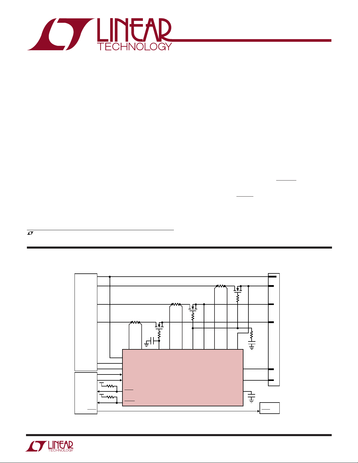
TYPICAL APPLICATIO
SYSTEM
POWER
SUPPLY
R8 10k
PCI
POWER
SYSTEM
CONTROLLER
RESET
R9 10k
U
R1
0.007Ω
R2
0.005Ω
R3
0.07Ω
11 10 9 13 14 15 3 17 16 18
AUXIN AUXSENSE AUXGATE 3VIN3V
8
GND
1
12V
IN
2
V
EEIN
12
AUXON
5
ON
6
FAULT
7
PWRGD
Si2306DS
C3
10nF
Q3
R6
10Ω
SENSE
LTC4241
Q2
IRF7413
R5
10Ω
GATE 3V
OUT5VIN5VSENSE5VOUT
Q1
IRF7413
12V
OUT
V
EEOUT
TIMER
R4
10Ω
GND
5V
5A
3.3V
7.6A
3.3V
AUX
500mA
R7
100Ω
C1
0.047µF
12V
20
500mA
–12V
19
100mA
4
C2
0.1µF
BACKPLANE
CONNECTOR
LOGIC
RESET
4241 F01
Figure 1. Hot Swappable PCI and 3.3V Auxiliary Supplies
sn4241 4241f
1
LTC4241
WW
W
U
ABSOLUTE AXI U RATI GS
(Note 1)
Supply Voltages
12VIN................................................................... 14V
V
.................................................................. –14V
EEIN
AUXIN ................................................................... 7V
Input Voltage
ON .........................................................–0.3V to 14V
AUXON ..................................................–0.3V to 14V
Output Voltages
(FAULT, PWRGD) ..................................–0.3V to 14V
Analog Voltages
TIMER, 3VIN, 3V
5V
3V
SENSE
, 5V
OUT
, 5V
.............................
IN
........................................–0.3V to 14V
OUT
AUXSENSE ..........................–0.3V to (AUXIN + 0.3V)
V
12V
................................................ –14V to + 0.3V
EEOUT
..................................................–0.3V to 14V
OUT
AUXGATE ......................... Internally Limited (Note 3)
Operating Temperature Range
LTC4241CGN........................................... 0°C to 70°C
LTC4241IGN........................................–40°C to 85°C
Storage Temperature Range ..................–65°C to 150°C
Lead Temperature (Soldering,10sec).................... 300°C
SENSE
, GATE,
–0.3V to (12VIN + 0.3V)
UUW
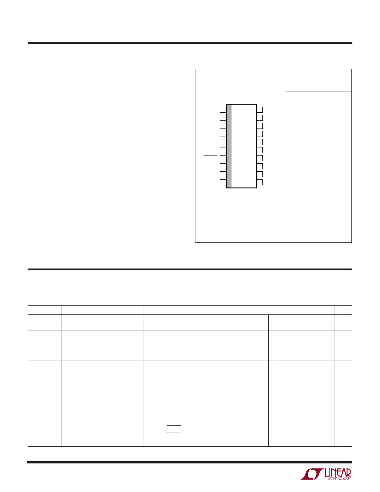
PACKAGE/ORDER I FOR ATIO
ORDER PART
NUMBER
TOP VIEW
1
12V
IN
2
V
EEIN
3
3V
OUT
4
TIMER
5
ON
6
FAULT
PWRGD
AUXGATE
AUXSENSE
Consult LTC Marketing for parts specified with wider operating temperature ranges.
7
8
GND
9
10
GN PACKAGE
20-LEAD NARROW PLASTIC SSOP
T
= 150°C, θJA = 135°C/W
JMAX
12V
20
OUT
V
19
EEOUT
5V
18
OUT
5V
17
IN
5V
16
SENSE
GATE
15
3V
14
SENSE
3V
13
IN
AUXON
12
AUXIN
11
LTC4241CGN
LTC4241IGN
DC ELECTRICAL CHARACTERISTICS
temperature range, otherwise specifications are at TA = 25°C. V
V
= 3.3V. (Note 2)
AUXIN
SYMBOL PARAMETER CONDITIONS MIN TYP MAX UNITS
I
DD
V
LKO
V
LKH
V
SENSE5(TH)
V
SENSE3(TH)
t
CB
I
GATE
V
Supply Current ON = V
12VIN
V
Supply Current AUXON = V
AUXIN
Undervoltage Lockout, 12V
Low-to-High Transition 3V
Undervoltage Lockout Hysteresis 3VIN, 5V
Current Limit Sense Voltage V
Threshold (V
Current Limit Sense Voltage V
Threshold (V
Circuit Breaker Trip Filter Time (V
GATE Pin Output Current ON High, FAULT High, V
5VIN
3VIN
– V
– V
)V
5VSENSE
)V
3VSENSE
12VIN
IN
IN
5V
IN
AUXIN
IN
AUXIN 120 mV
= 0V ● 5.5 9 14.5 mV
5VOUT
> 4V ● 40 55 70 mV
5VOUT
= 0V ● 5.5 9 14.5 mV
3VOUT
> 2V ● 40 55 70 mV
3VOUT
– V
5VIN
(V
– V
AUXIN
ON Low, FAULT High, V
ON High, FAULT Low, V
The ● denotes the specifications which apply over the full operating
= 12V, V
12VIN
AUXIN
) = Step 0 to 100mV 17 µs
5VSENSE
AUXSENSE
) = Step 0 to 100mV 8 µs
= GND ● –20 –60 –100 µA
GATE
= 5V 200 µA
GATE
= 5V 5 25 35 mA
GATE
VEEIN
= –12V, V
= 3.3V, V
3VIN
= 5V,
5VIN
● 2.5 8 mA
● 0.5 1.5 mA
● 6.5 9 10.8 V
● 2.25 2.50 2.75 V
● 3.65 3.90 4.15 V
● 2.35 2.60 2.85 V
20 mV
sn4241 4241f
2
LTC4241
DC ELECTRICAL CHARACTERISTICS
temperature range, otherwise specifications are at TA = 25°C. V
V
= 3.3V. (Note 2)
AUXIN
The ● denotes the specifications which apply over the full operating
12VIN
= 12V, V
VEEIN
= –12V, V
= 3.3V, V
3VIN
5VIN
= 5V,
SYMBOL PARAMETER CONDITIONS MIN TYP MAX UNITS
∆V
GATE
V
DROP
I
CL(12)
I
CL(VEE)
T
TS
V
PG(TH)
V
PGH
V
IL
V
IH
V
OL
I
IN
External Gate Voltage (V
Internal Switch Voltage Drop (V
Current Limit 12VIN = 12V, 12V
Current Limit V
(V
12V
EEIN
V
EEIN
12VIN
12VIN
EEOUT
– V
GATE
– V
12VOUT
– V
= 12V, 12V
IN
= –12V, V
= –12V, V
) ● 100 200 mV
VEEIN
), I
), I
OUT
OUT
EEOUT
EEOUT
= 500mA ● 200 600 mV
12VOUT
= 100mA ● 120 250 mV
VEEIN
= 0V, TIMER = GND ● –50 –300 –575 mA
= 11V, TIMER = GND ● –525 –850 –1500 mA
= 0V, TIMER = GND ● 50 200 425 mA
= –11V, TIMER = GND ● 250 450 750 mA
Thermal Shutdown Temperature 150 °C
Power Good Threshold Voltage V
Power Good Hysteresis 3V
Rising ● 10.8 11.1 11.4 V
12VOUT
V
Falling ● –10.2 –10.5 –10.8 V
VEEOUT
Rising ● 2.8 2.9 3.0 V
V
3VOUT
Rising ● 4.5 4.65 4.78 V
V
5VOUT
5V
12V
OUT
OUT
OUT
, V
EEOUT
20 mV
30 mV
50 mV
Input Low Voltage ON, AUXON ● 0.8 V
Input High Voltage ON, AUXON ● 2V
Output Low Voltage FAULT, PWRGD , IOL = 3mA ● 0.4 V
AUXON Pin Input Current AUXON = GND ● ±0.08 ±10 µA
AUXON = V
AUXIN
● ±0.08 ±10 µA
ON Pin Input Current ON = GND ● ±0.08 ±10 µA
● ±0.08 ±10 µA
5V
Input Current 5V
SENSE
3V
Input Current 3V
SENSE
ON = V
12VIN
= 5V ● 50 100 µA
SENSE
= 3V ● 50 100 µA
SENSE
5VIN Input Current 5VIN = 5V ● 580 900 µA
3VIN Input Current 3VIN = 3V ● 310 550 µA
5V
R
DIS
I
TIMER
V
TIMER
V
AUXCB
I
AUXGATE
∆V
AUXGATE
Input Current 5V
OUT
3V
Input Current 3V
OUT
5V
Discharge Impedance ON = GND 60 Ω
OUT
3V
Discharge Impedance ON = GND 50 Ω
OUT
Discharge Impedance ON = GND 450 Ω
12V
OUT
Discharge Impedance ON = GND 1600 Ω
V
EEOUT
TIMER Pin Current Timer On, V
TIMER Threshold Voltage
(V
12VIN
– V
) ● 0.5 0.9 1.3 V
TIMER
Circuit Breaker Trip Voltage
(V
AUXIN
– V
AUXSENSE
) ● 40 50 60 mV
AUXGATE Gate Output Current AUXON High, FAULT High, V
External AUXGATE Gate Voltage (V
= 5V, ON = V
OUT
= 3V, ON = V
OUT
Timer Off, V
12VIN
12VIN
= GND, ● –15 –22 –27 µA
TIMER
= 5V, 45 mA
TIMER
AUXON Low, FAULT High, V
AUXON High, FAULT Low, V
AUXGATE
– V
AUXIN
), V
AUXIN
● 260 500 µA
● 150 350 µA
= GND ● –6 –10 –14 µA
AUXGATE
= 5V 200 µA
AUXGATE
= 10V 50 mA
AUXGATE
= 3.3V ● 5811 V
Note 1: Absolute Maximum Ratings are those values beyond which the life
of a device may be impaired.
Note 2 : All currents into device pins are positive; all currents out of device
pins are negative. All voltages are referenced to ground unless otherwise
specified.
Note 3 : An internal zener on the AUXGATE pin clamps the charge pump
voltage to a typical maximum operating voltage of 12V. External overdrive
of the AUXGATE pin beyond the internal zener voltage may damage the
device.
sn4241 4241f
3
LTC4241
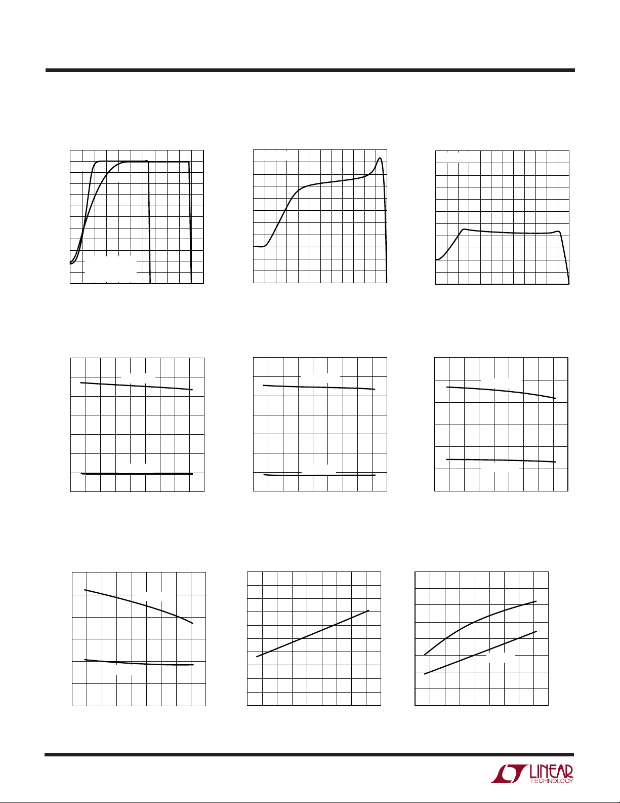
TEMPERATURE (°C)
–75 –50 –25
CURRENT LIMIT (mA)
25 500
1200
1000
800
600
400
200
0
4241 • G06
125 15075 100
12V
OUT
= 11V
12V
OUT
= 0V
UW
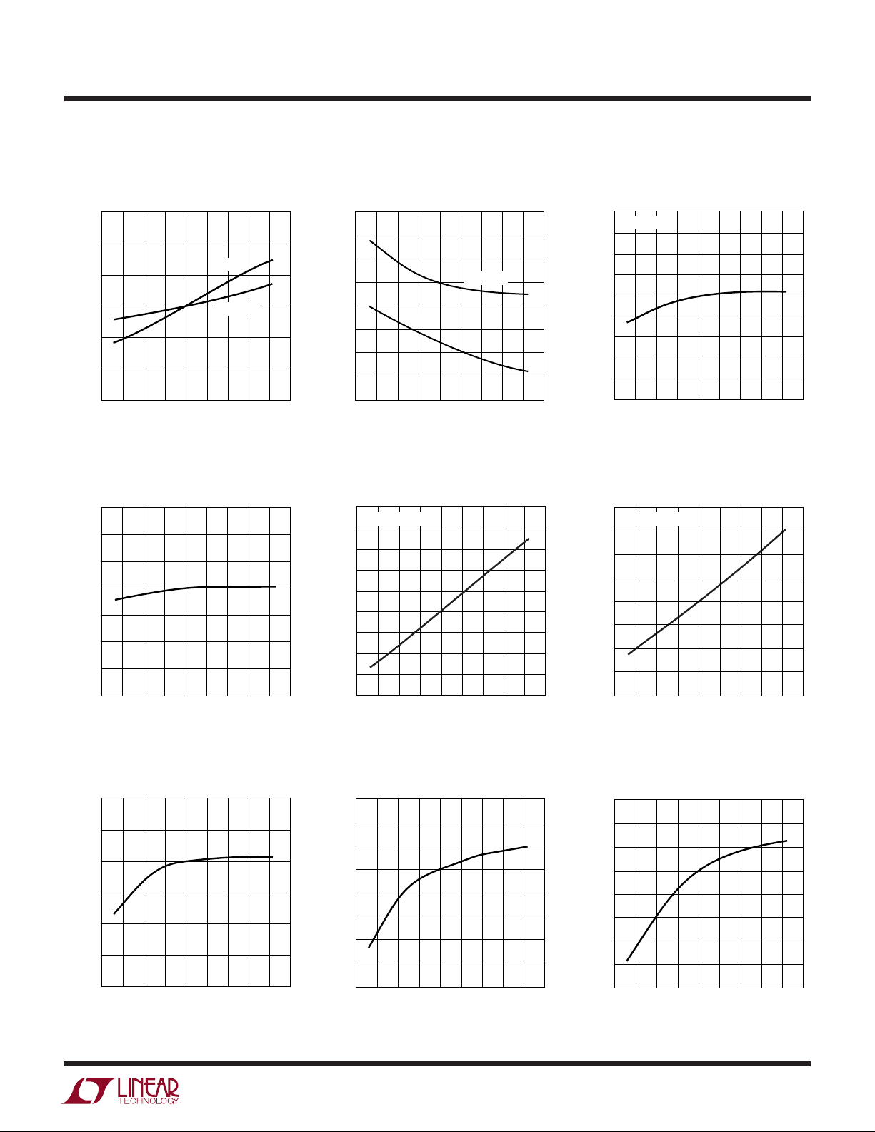
TYPICAL PERFOR A CE CHARACTERISTICS
3.3V and 5V Current
Foldback Profile
12
3V
OUT
10
8
6
4
OUTPUT CURRENT (A)
3VIN = 3.3V
2
0
= 5V
5V
IN
R
= 0.005Ω
SENSE
0.5
OUTPUT VOLTAGE (V)
5V
OUT
2.51.5 3.5 4.5
5.5
4241 • G01
12V Current Foldback Profile
1100
12VIN = 12V
1000
900
800
700
600
500
400
300
OUTPUT CURRENT (mA)
200
100
0
0 1 2 3 4 5 6 7 8 9 10 11 12
OUTPUT VOLTAGE (V)
4241 • G02
–12V Current Foldback Profile
1100
V
= –12V
EEIN
1000
900
800
700
600
500
400
300
OUTPUT CURRENT (mA)
200
100
0
0 –1 –2 –3 –4 –5 –6 –7 –8 –9 –10 –11–12
OUTPUT VOLTAGE (V)
4241 • G03
70
60
50
40
30
20
CURRENT LIMIT VOLTAGE (mV)
10
600
500
400
300
200
CURRENT LIMIT (mA)
100
5VIN Current Limit Voltage
vs Temperature
5V
= 5V
OUT
5V
= 0V
OUT
0
–75 –50 –25
V
Current Limit
EEIN
25 500
TEMPERATURE (°C)
vs Temperature
V
= –11V
EEOUT
V
= 0V
EEOUT
0
–75 –50 –25
25 500
TEMPERATURE (°C)
125 15075 100
4241 • G04
125 15075 100
4241 • G07
3VIN Current Limit Voltage
vs Temperature
70
60
50
40
30
20
CURRENT LIMIT VOLTAGE (mV)
10
0
–75 –50 –25
(V
AUXIN
3V
3V
TEMPERATURE (°C)
– V
AUXSENSE
OUT
OUT
25 500
= 3.3V
= 0V
)
Circuit Breaker Trip Voltage
vs Temperature
55
54
53
52
51
50
49
48
47
46
CIRCUIT BREAKER TRIP VOLTAGE (mV)
45
–75 –50 –25
25 500
TEMPERATURE (°C)
125 15075 100
4241 • G05
125 15075 100
4241 • G08
12VIN Current Limit
vs Temperature
GATE, AUXGATE Output Source
Current vs Temperature
90
80
70
60
50
40
30
20
GATE OUTPUT SOURCE CURRENT (µA)
10
–75 –50 –25
GATE
AUXGATE
25 500
TEMPERATURE (°C)
125 15075 100
4241 • G09
sn4241 4241f
12.5
12.0
11.5
11.0
10.5
10.0
9.5
9.0
8.5
AUXGATE OUTPUT SOURCE CURRENT (µA)
4
UW
TYPICAL PERFOR A CE CHARACTERISTICS
LTC4241
GATE, AUXGATE Output Sink
Current vs Temperature
350
300
250
200
150
OUTPUT SINK CURRENT (µA)
100
50
–75 –50 –25
TEMPERATURE (°C)
GATE
AUXGATE
25 500
AUXGATE Voltage vs Temperature
11.75
11.60
11.45
11.30
11.15
11.00
AUXGATE VOLTAGE (V)
10.85
10.70
–75 –50 –25
25 500
TEMPERATURE (°C)
125 15075 100
4241 • G10
125 15075 100
4241 • G13
GATE, AUXGATE Fast Pull-Down
Current vs Temperature
80
70
60
50
40
30
20
FAST PULL-DOWN CURRENT (mA)
10
0
–75 –50 –25
GATE
TEMPERATURE (°C)
AUXGATE
25 500
12V Internal Switch Voltage Drop
vs Temperature
325
I
= 500mA
12VOUT
300
275
250
225
200
175
150
125
INTERNAL SWITCH VOLTAGE DROP (mV)
100
–75 –50 –25
25 500
TEMPERATURE (°C)
125 15075 100
4241 • G11
125 15075 100
4241 • G14
(V
AUXGATE
– V
AUXIN
)
vs Temperature
8.20
AUXIN = 3.3V
8.15
8.10
) (V)
8.05
AUXIN
8.00
– V
7.95
7.90
AUXGATE
(V
7.85
7.80
7.75
–75 –50 –25
25 500
TEMPERATURE (°C)
VEE Internal Switch Voltage Drop
vs Temperature
200
I
= 100mA
VEEIN
180
160
140
120
100
80
60
INTERNAL SWITCH VOLTAGE DROP (mV)
40
–75 –50 –25
25 500
TEMPERATURE (°C)
125 15075 100
4241 • G12
125 15075 100
4241 • G15
Power Good Threshold Voltage
vs Temperature (12V
11.20
11.15
11.10
11.05
11.00
10.95
POWER GOOD THRESHOLD VOLTAGE (V)
10.90
–75 –50 –25
TEMPERATURE (°C)
OUT
25 500
Power Good Threshold Voltage
)
125 15075 100
4241 • G16
vs Temperature (5V
4.68
4.67
4.66
4.65
4.64
4.63
4.62
4.61
POWER GOOD THRESHOLD VOLTAGE (V)
4.60
–75 –50 –25
TEMPERATURE (°C)
OUT
25 500
)
125 15075 100
4241 • G17
Power Good Threshold Voltage
vs Temperature (3V
2.915
2.910
2.905
2.900
2.895
2.890
2.885
2.880
POWER GOOD THRESHOLD VOLTAGE (V)
2.875
–75 –50 –25
TEMPERATURE (°C)
OUT
25 500
)
125 15075 100
4241 • G18
sn4241 4241f
5

LTC4241
TEMPERATURE (°C)
–75 –50 –25
TIMER CURRENT (µA)
25 500
23.00
22.75
22.50
22.25
22.00
21.75
21.50
21.25
21.00
4241 • G21
125 15075 100
TEMPERATURE (°C)
–75 –50 –25
(V
5VIN
– V
5VSENSE
) CIRCUIT BREAKER TRIP
FILTER TIME (µs)
(V
AUXIN
– V
AUXSENSE
) CIRCUIT BREAKER TRIP
FILTER TIME (µs)
25 500
18.50
18.25
18.00
17.75
17.50
17.25
17.00
16.75
16.50
8.3
8.2
8.1
8.0
7.9
7.8
7.7
7.6
7.5
4241 • G27
125 15075 100
V
AUXIN
– V
AUXSENSE
V
5VIN
– V
5VSENSE
UW
TYPICAL PERFOR A CE CHARACTERISTICS
Power Good Threshold Voltage
vs Temperature (V
–10.60
–10.55
–10.50
–10.45
–10.40
–10.35
POWER GOOD THRESHOLD VOLTAGE (V)
–10.30
–75 –50 –25
TEMPERATURE (°C)
EEOUT
25 500
12VIN Supply Current
vs Temperature
2.9
2.8
2.7
2.6
2.5
2.4
SUPPLY CURRENT (mA)
2.3
2.2
–75 –50 –25
25 500
TEMPERATURE (°C)
Timer Threshold Voltage
)
125 15075 100
4241 • G19
vs Temperature
0.950
V
– V
12VIN
0.925
0.900
0.875
0.850
0.825
0.800
TIMER THRESHOLD VOLTAGE (V)
0.775
0.750
–75 –50 –25
V
TIMER
25 500
TEMPERATURE (°C)
, 5VIN, 3VIN, AUXIN Supply
EEIN
125 15075 100
4241 • G20
Current vs Temperature
700
125 15075 100
4241 • G22
650
600
550
500
450
400
350
SUPPLY CURRENT (µA)
300
250
200
3V
–75 –50 –25
AUXIN
V
EEIN
IN
25 500
TEMPERATURE (°C)
5V
IN
125 15075 100
4241 • G23
Timer Current vs Temperature
12VIN Undervoltage Lockout
Threshold vs Temperature
9.20
9.15
9.10
9.05
9.00
8.95
8.90
8.85
UNDERVOLTAGE LOCKOUT THRESHOLD (V)
8.80
–75 –50 –25
25 500
TEMPERATURE (°C)
125 15075 100
4241 • G24
5VIN Undervoltage Lockout
Threshold vs Temperature
3.950
3.925
3.900
3.875
3.850
3.825
UNDERVOLTAGE LOCKOUT THRESHOLD (V)
3.800
–75 –50 –25
6
TEMPERATURE (°C)
(V
– V
3VIN, AUXIN Undervoltage Lockout
Threshold vs Temperature
2.650
2.625
2.600
2.575
2.550
2.525
25 500
125 15075 100
4241 • G25
2.500
2.475
UNDERVOLTAGE LOCKOUT THRESHOLD (V)
2.450
–75 –50 –25
AUXIN
3V
IN
25 500
TEMPERATURE (°C)
125 15075 100
4241 • G26
5VIN
V
AUXSENSE
Filter Time vs Temperature
5VSENSE
), (V
AUXIN
–
) Circuit Breaker Trip
sn4241 4241f

LTC4241
U
UU
PI FU CTIO S
12VIN (Pin 1): 12V Supply Input. This pin powers the
primary controller internal circuitry. A 0.5Ω switch is
connected between 12V
current limit. An undervoltage lockout circuit prevents the
switches from turning on while the 12VIN pin voltage is
less than 9V.
V
(Pin 2): –12V Supply Input. A 1.2Ω switch is
EEIN
connected between V
current limit.
3V
(Pin 3): 3.3V Output Monitor. Used to monitor the
OUT
3.3V output supply voltage. The PWRGD signal cannot go
low until the 3V
TIMER (Pin 4): Current Limit Fault Timer Input. Connect a
capacitor from TIMER to ground. With the primary controller turned off (ON = GND) or the internal circuit breaker
tripped due to a PCI supply fault (FAULT = low), the TIMER
pin is internally held at ground. When the primary controller is turned on, a 22µA pull-up current source is con-
nected to TIMER. Current limit faults from the PCI supplies
will be ignored until the voltage at the TIMER pin rises to
within 0.9V of 12VIN.
pin exceeds 2.9V.
OUT
EEIN
and 12V
IN
and V
with a foldback
OUT
with a foldback
EEOUT
power good threshold voltage, PWRGD will go high after
a 15µs deglitching time. The switches will not be turned off
when PWRGD goes high.
GND (Pin 8): Chip Ground
AUXGATE (Pin 9): High Side Gate Drive for the 3.3V
Auxiliary External N-channel MOSFET. An internal charge
pump generates at least 8V of gate drive from a 3.3V
auxiliary supply. A zener clamps AUXGATE approximately
12V above the supply voltage at AUXIN. The rise time at
AUXGATE is set by an external AUXGATE capacitor connected to ground and an internal 10µA current source
provided by the charge pump. If the circuit breaker trips or
the auxiliary supply voltage hits the undervoltage lockout
threshold, a 50mA current sink rapidly pulls AUXGATE
low.
AUXSENSE (Pin 10): 3.3V Auxiliary Circuit Breaker Current Sense Input. The load current is monitored by a sense
resistor connected between AUXIN and AUXSENSE. The
circuit breaker trips if the voltage across the sense resistor
exceeds 50mV and the AUXGATE pin voltage will be turned
off.
ON (Pin 5): On Control Input. A rising edge turns on the
external N-channel FETs for 3.3V and 5V PCI supplies, the
internal 12V and –12V switches and a falling edge turns it
off. If the ON pin is cycled low then high following the trip
of the circuit breaker due to a PCI supply fault, the circuit
breaker is reset.
FAULT (Pin 6): Fault Output. Open drain logic output used
by both the primary and auxiliary controller to indicate an
overcurrent fault condition. When any of the PCI and 3.3V
auxiliary supplies are in current limit fault, the controller
detecting the fault (primary or auxiliary) will be latched off
and the FAULT pin will be pulled low. Current limit faults
from the PCI supplies are ignored while the voltage at the
TIMER pin is less than (12VIN – 0.9V). The current limit
fault detected by the primary controller will not cause the
auxiliary controller to latch off and vice versa.
PWRGD (Pin 7): Power Good Output. Open drain logic
output used by the primary controller to indicate the
voltage status of the PCI supplies. PWRGD remains low
while V
V
VEEOUT
≥ 11.1V, V
12VOUT
≤ –10.5V. When one of the supplies falls below its
3VOUT
≥ 2.9V, V
5VOUT
≥ 4.65V,
AUXIN (Pin 11): 3.3V Auxiliary Supply Input. This pin
powers the auxiliary controller internal circuitry. An
undervoltage lockout circuit disables the AUXGATE pin
until the supply voltage at AUXIN is greater than 2.6V.
AUXGATE is held at ground potential until the undervoltage
lockout deactivates. If no 3.3V auxiliary supply is available,
tie AUXIN to ground.
AUXON (Pin 12): ON Control Input for Auxiliary Supply. A
rising edge turns on the external N-channel FET for 3.3V
auxiliary supply and a falling edge turns it off. If the AUXON
pin is cycled low then high following the trip of the circuit
breaker due to a 3.3V auxiliary supply fault, the circuit
breaker is reset.
3VIN (Pin 13): 3.3V Supply Sense Input. An undervoltage
lockout circuit prevents the switches from turning on
when the voltage at the 3VIN pin is less than 2.5V. If no 3.3V
input supply is available, tie 3VIN to the 5VIN pin.
3V
resistor placed in the supply path between 3VIN and
3V
(Pin 14): 3.3V Current Limit Set Pin. With a sense
SENSE
, the GATE pin voltage will be adjusted to maintain
SENSE
sn4241 4241f
7

LTC4241
U
UU
PI FU CTIO S
a constant voltage across the sense resistor and a
constant current through the switch. A foldback feature
makes the current limit decrease as the voltage at the
3V
pin approaches ground. To disable the current limit,
OUT
3V
GATE (Pin 15): High Side Gate Drive for the 3.3V and 5V
PCI Supplies External N-channel MOSFETs. Requires an
external series RC network for the current limit loop
compensation and setting the minimum ramp-up rate.
During power-up, the slope of the voltage rise at the GATE
is set by the internal 60µA pull up current source and the
external GATE capacitor connected to ground. During
power-down, the slope of the falling voltage is set by the
200µA current source connected to ground and the exter-
nal GATE capacitor.
5V
resistor placed in the supply path between 5VIN and
5V
a constant voltage across the sense resistor and a constant current through the switch. A foldback feature makes
and 3VIN can be shorted together.
SENSE
(Pin 16): 5V Current Limit Set Pin. With a sense
SENSE
, the GATE pin voltage will be adjusted to maintain
SENSE
the current limit decrease as the voltage at the 5V
approaches ground. To disable the current limit, 5V
and 5VIN can be shorted together.
5VIN (Pin 17): 5V Supply Sense Input. Used to monitor the
5V input supply voltage. An undervoltage lockout circuit
prevents the switches from turning on when the voltage at
the 5VIN pin is less than 3.9V.
5V
(Pin 18): 5V Output Monitor. Used to monitor the
OUT
5V output supply voltage. The PWRGD signal cannot go
low until the 5V
V
connected between V
fall below –10.5V before the PWRGD signal can go low on
the LTC4241.
12V
connected between 12VIN and 12V
exceed 11.1V before the PWRGD signal can go low on the
LTC4241
(Pin 19): –12V Supply Output. A 1.2Ω switch is
EEOUT
(Pin 20): 12V Supply Output. A 0.5Ω switch is
OUT
pin exceeds 4.65V.
OUT
and V
EEIN
EEOUT
OUT
. V
EEOUT
. 12V
OUT
pin
OUT
SENSE
must
must
8
sn4241 4241f

BLOCK DIAGRA
LTC4241
W
PWRGD
FAULT
5VIN5V
SENSE
17 16 15 14 13 183
+
5V
OUT
–
+
55mV
+
5
ON
3.9V
UVL
A1
–
–
GATE 3V
12V
IN
60µA
Q5
200µA
+
A2
–
SENSE
55mV
–
3V
IN
+
3V
OUT
–
+
2.5V
UVL
C
P1
3V
OUT5VOUT
Q8
Q7
+
7
Q3
6
Q4
PRIMARY CONTROL LOGIC
–
REF
CP2
+
–
9V
UVL
Q1
1 20
12V
IN
12V
OUT
REF
12V
Q9
CP4 CP3
+
IN
22µA
Q6
–
4 2 19
TIMER V
EEIN
REF
Q2
Q10
REF
+
V
EEOUT
–
8
GND
PCI-BUS HOT SWAP
CONTROLLER
AUXIN
AUXSENSE
AUXON
Q12
11
+
50mV
–
10
12
+
A3
8µs
FILTER
–
2.6V
UVL
AUXILIARY
CONTROL
LOGIC
CHARGE
PUMP
Q11
10µA
Z1
200µA
12V
AUXIN
3.3V AUXILIARY SUPPLY
HOT SWAP CONTROLLER
Z2
20V
9
4241 BD
AUXGATE
sn4241 4241f
9

LTC4241
WUUU
APPLICATIO S I FOR ATIO
Hot Circuit Insertion
When a circuit board is inserted into a live PCI slot, the
supply bypass capacitors on the board can draw huge
transient currents from the PCI power bus as they charge
up. The transient currents can cause permanent damage
to the connector pins and glitches the power bus, causing
other boards in the system to reset.
The LTC4241 is designed to turn a board’s supply voltages
on and off in a controlled manner, allowing the board to be
safely inserted or removed from a live PCI slot without
glitching the system power supplies. The chip also protects the PCI supplies from shorts and monitors the
supply voltages.
The LTC4241 is designed for motherboard applications
and includes an additional independent controller for the
3.3V auxiliary supply.
LTC4241 Feature Summary
1. Allows safe board insertion and removal from a
motherboard.
2. Primary controller to control the four PCI supplies:
3.3V, 5V, –12V, 12V and an independent auxiliary controller to control the 3.3V auxiliary supply.
3. Adjustable foldback current limit for PCI supplies: an
adjustable analog current limit with a value that depends
on the output voltage. If the output is shorted to ground,
the current limit drops to keep power dissipation and
supply glitches to a minimum.
4. Electronic circuit breaker for all supplies: if a supply
remains in current limit for too long, the circuit breaker will
trip, the supplies will be turned off and the FAULT pin
pulled low.
5. Current limit power-up: the four PCI supplies are
allowed to power up in current limit. This allows the chip
to power up boards with a wide range of capacitive loads
without tripping the circuit breaker. The maximum allowable power-up time is programmable using the TIMER pin.
6. On-Chip –12V and 12V power switches
7. Power good output: monitors the voltage status of the
four PCI supply voltages. The 3.3V auxiliary supply is not
monitored.
8. Fault control: the current limit fault detected by either
the primary or auxiliary controller will not cause the other
controller to latch off. Both controllers use the FAULT
output to indicate a fault condition.
9. Space saving 20-pin narrow SSOP package.
PCI Power Requirements
PCI systems usually require four power rails: 5V, 3.3V,
–12V and 12V. Systems implementing the 3.3V signaling
environment are usually required to provide all four rails in
every system.
A 3.3V auxiliary supply is added in the PCI system to power
PCI logic functions that need to remain active when the
rest of the system is unpowered.
The tolerance of the supplies as measured at the components is summarized in Table 1.
Table 1. PCI Power Supply Requirements
CAPACITIVE
SUPPLY TOLERANCE LOAD
5V 5V ± 5% <3000µF
3.3V 3.3V ± 0.3V <3000µF
12V 12V ± 5% <500µF
–12V –12V ± 10% <120µF
3.3V
AUX
3.3V ± 0.3V <500µF
Power-Up Sequence for PCI Power Supplies
The PCI power supplies are controlled by placing external
N-channel pass transistors in the 3.3V and 5V power
paths, and internal pass transistors for the 12V and –12V
power paths (Figure 1).
Resistors R1 and R2 provide a current signal for fault
detection and R7 and C1 provide current control loop
compensation. Resistors R4 and R5 prevent high frequency oscillations in Q1 and Q2.
When the ON pin is pulled high, the GATE pin is pulled high
by an internal 60µA current source and the pass transis-
tors are allowed to turn on. The internal 12V and –12V
switches are also turned on and a 22µA current source is
connected to the TIMER pin (Figure 2).
sn4241 4241f
10

t
CV
II
ON
LOAD OUT
LIMIT LOAD
≅
2•
•
–
WUUU
APPLICATIO S I FOR ATIO
LTC4241
ON
10V/DIV
TIMER
10V/DIV
GATE
10V/DIV
12V
OUT
5V/DIV
5V/DIV
5V
OUT
3V
5V/DIV
OUT
V
EEOUT
5V/DIV
FAULT
10V/DIV
PWRGD
10V/DIV
10ms/DIV
Figure 2. Normal Power-Up Sequence
4241 F02
The current in each pass transistor increases until it
reaches the current limit for each supply. Each supply is
allowed to power up at the rate dV/dt = 60µA/C1 or as
determined by the current limit and the load capacitance
on the supply line, whichever is slower. Current limit faults
are ignored while the TIMER pin voltage is ramping up and
is less than 0.9V below 12VIN. Once all four PCI supply
voltages are within tolerance, the PWRGD pin will pull low.
ON
10V/DIV
TIMER
10V/DIV
GATE
10V/DIV
12V
OUT
5V/DIV
5V/DIV
5V
OUT
3V
5V/DIV
OUT
V
EEOUT
5V/DIV
FAULT
10V/DIV
PWRGD
10V/DIV
10ms/DIV
Figure 3. Normal Power-Down Sequence
4241 F03
Timer
During a power-up sequence for the PCI power supplies,
a 22µA current source is connected to the TIMER pin and
current limit faults are ignored until the voltage ramps to
within 0.9V of 12VIN. This feature allows the chip to power
up a PCI slot that can accommodate boards with a wide
range of capacitive loads on the supplies. The power-up
time for any one of the four outputs will be:
Power-Down Sequence for PCI Power Supplies
When the ON pin is pulled low, a power-down sequence
begins for all the PCI power supplies (Figure 3).
Internal switches are connected to each of the output
supply voltage pins to discharge the load capacitors to
ground. The TIMER pin is immediately pulled low and the
internal 12V and –12V switches are turned off. The GATE
pin is pulled to ground by an internal 200µA current
source. This turns off the external pass transistors in a
controlled manner and prevents the load current on the
3.3V and 5V supplies from going to zero instantaneously
and glitching the power supply voltages. When any of the
output voltages dips below its threshold, the PWRGD pin
pulls high.
For example, for C
I
= 5A, the 5V
LOAD
= 2000µF, V
LOAD
turn-on time will be ~10ms. By
OUT
OUT
= 5V, I
LIMIT
= 7A,
substituting the variables in the above equation with the
appropriate values, the turn-on time for the other three
outputs can be calculated. The timer period should be set
longer than the maximum supply turn-on time but short
enough to not exceed the maximum safe operating area of
the pass transistor during a short-circuit. The timer period
is given by:
t
TIMER
CV
=
TIMER
22
•.11 1
A
µ
sn4241 4241f
11

LTC4241
WUUU
APPLICATIO S I FOR ATIO
For C
= 0.1µF, the timer period will be ~50ms. The
TIMER
TIMER pin is immediately pulled low when ON goes low.
Thermal Shutdown
The internal switches for the 12V and –12V supplies are
protected by an internal current limit and thermal shutdown circuit. When the temperature of the chip reaches
150°C, only the switches controlling the PCI supplies will
be latched off and the FAULT pin will be pulled low.
Short-Circuit Protection for PCI Power Supplies
During a normal power-up sequence for the PCI power
supplies, if the TIMER is done ramping and any supply is
still in current limit, all of the pass transistors will be
immediately turned off, the TIMER and FAULT pin will be
pulled low as shown in Figure 4.
ON
10V/DIV
TIMER
10V/DIV
spikes — for example, from a fan turning on — from
causing false trips of the circuit breaker. The chip will stay
in the latched-off state until the ON pin is cycled low then
high, or the 12VIN supply is cycled.
To prevent excessive power dissipation in the pass transistors and to prevent voltage spikes on the supplies
during short-circuit conditions, the current limit on each
PCI supply, except the 3.3V auxiliary supply, is designed
to be a function of the output voltage. As the output voltage
drops, the current limit decreases. Unlike a traditional
circuit breaker function where huge currents can flow
before the breaker trips, the current foldback feature
assures that the supply current will be kept at a safe level
and prevent voltage glitches when powering up into a
short.
ON
10V/DIV
TIMER
10V/DIV
GATE
10V/DIV
12V
OUT
5V/DIV
5V/DIV
5V
OUT
3V
5V/DIV
OUT
V
EEOUT
5V/DIV
FAULT
10V/DIV
PWRGD
10V/DIV
20ms/DIV
4241 F04
Figure 4. Power-Up into a Short on 3.3V Output
If a short-circuit occurs after the PCI supplies are powered
up, the shorted supply’s current will drop immediately to
the limit value (Figure 5).
If the supply remains in current limit for more than 17µs,
all of the PCI supplies except the 3.3V auxiliary supply will
be latched off. The 17µs delay prevents quick current
GATE
10V/DIV
12V
OUT
5V/DIV
5V/DIV
5V
OUT
3V
5V/DIV
OUT
V
EEOUT
5V/DIV
FAULT
10V/DIV
PWRGD
10V/DIV
20ms/DIV
4241 F05
Figure 5. Short-Circuit on 5V Followed by Circuit Breaker Reset
The current limit and the foldback current level for the 5V
and 3.3V outputs are both a function of the external sense
resistor (R1 for 5V
and R2 for 3V
OUT
, see Figure 1). As
OUT
shown in Figure 1, a sense resistor is connected between
5VIN and 5V
sense resistor is connected between 3VIN and 3V
for the 5V supply. For the 3V supply, a
SENSE
SENSE
sn4241 4241f
.
12

WUUU
APPLICATIO S I FOR ATIO
LTC4241
The current limit and the foldback current level (at the
V
= 0V) are given by:
OUT
I
= 55mV/R
LIMIT
I
FOLDBACK
SENSE
= 9mV/R
SENSE
As a design aid, the current limit and foldback level for
commonly used values for R
Table 2. I
R
and I
LIMIT
SENSE
0.005 11A 1.8A
0.006 9.2A 1.5A
0.007 7.9A 1.3A
0.008 6.9A 1.1A
0.009 6.1A 1.0A
0.01 5.5A 0.9A
FOLDBACK
(Ω)I
vs R
LIMIT
are given in Table 2.
SENSE
SENSE
I
FOLDBACK
The current limit for the internal 12V switch is set at
850mA folding back to 300mA and the –12V switch at
450mA folding back to 200mA.
In systems where it is possible to exceed the current limit
for a short amount of time, it might be necessary to
prevent the analog current loop from responding quickly
so the output voltage does not droop. This can be accomplished by adding an RC filter across the sense resistor as
shown in Figure 6. RF should be 20Ω or less to prevent
offset errors. A capacitor, CF, of 0.1µF gives a delay of
about 1.5µs and a 1µF capacitor gives a delay of about
15µs.
21
43
R
20Ω
IRF7413
F
Q1
5V
OUT
5A
R4
10Ω
R1
5V
0.007Ω
IN
C
F
1µF
power path (Figure 1). The resistor R3 provides load
current fault detection and R6 prevents high frequency
oscillation in Q3.
When power is first applied to V
, the AUXGATE pin
AUXIN
pulls low. A low-to-high transition at the AUXON pin
initiates the AUXGATE ramp up (Figure 7). The AUXGATE
is pulled high by an internal 10µA current source and the
pass transistor is allowed to turn on. As the auxiliary
controller does not have the foldback current limit feature
and timer control, the inrush supply current during powerup is limited by ramping the gate of the pass transistor at
a controlled rate (dV/dt = 10µA/C3) where C3 is the total
external capacitance between AUXGATE and ground.
With proper selection of the C3 capacitance value, the
inrush current (I = C
• dV/dt = 10µA • C
LOAD
LOAD
/C3) is
limited to a value less than the current limit set by the sense
resistor R3. This prevents the circuit breaker from tripping
during power-up. C
is the total load capacitance on
LOAD
the 3.3V auxiliary supply line. For example, for C3 = 10nF,
C
= 470µF, R3 = 0.07Ω, I
LOAD
current will be 0.47A < I
3.3V
t = (V
output to reach its final value is equal to
AUX
• C3)/10µA.
AUXIN
LIMIT
= 0.7A, the inrush
LIMIT
. The ramp-up time for
A high-to-low transition at the AUXON pin initiates a
AUXGATE ramp-down at a slope of –200µA/C3 as the
AUXGATE is pulled to ground by an internal 200µA current
source. This will allow the load capacitance on the supply
line to discharge while the AUXGATE pulls low to turn off
the external N-channel pass transistor.
AUXON
2V/DIV
R7
OUT
100Ω
C1
0.047µF
17 16 15 18
5V
*ADDITIONAL PINS
OMITTED FOR
CLARITY
Figure 6. Delay in the Current Limit Loop
IN5VSENSE
GATE 5V
LTC4241*
Power-Up/Down Sequence for 3.3V Auxiliary Supply
The 3.3V auxiliary supply is controlled by placing an
external N-channel pass transistor Q3 in the 3.3V
AUX
AUXGATE
5V/DIV
3.3V
AUX
2V/DIV
5ms/DIV
Figure 7. Power-Up/Down Sequence for 3.3V Auxiliary Supply
4241 F07
sn4241 4241f
13

LTC4241
WUUU
APPLICATIO S I FOR ATIO
Electronic Circuit Breaker for 3.3V Auxiliary Supply
An electronic circuit breaker is used to protect against
excessive load current and short-circuits on the 3.3V
auxiliary supply. The load current is monitored by placing
a sense resistor R3 between AUXIN and AUXSENSE as
shown in Figure 1. The circuit breaker trip threshold is
50mV and exhibits a response time of 8µs. Unlike the PCI
supplies which use the current foldback limit with circuit
breaker during short-circuits, here the circuit breaker will
trip and immediately pull AUXGATE to ground if the
voltage between AUXIN and AUXSENSE exceeds 50mV for
Supply Bypass Capacitors
In motherboard applications, large bypass capacitors are
recommended at each of the system power supplies to
minimize supply glitches as a result of board insertion. A
supply bypass capacitor of ≥100µF at 12VIN connection is
recommended.
CURRENT FLOW
FROM SUPPLY
TRACK WIDTH W:
0.03" PER AMPERE
ON 1 OZ COPPER FOIL
SENSE RESISTOR
W
CURRENT FLOW
TO LOAD
more than 8µs. The external N-channel transistor is turned
off and FAULT is pulled low. The circuit breaker is reset
when AUXON is cycled low then high, or the AUXIN supply
is cycled. If the circuit breaker feature is not required, the
AUXSENSE pin can be shorted to AUXIN.
5V
IN
Figure 8. Making PCB Connections to
the Sense Resistor for the 5V Rail
5V
SENSE
The trip current of the circuit breaker is set by:
PCB Layout Considerations for the Sense Resistor
I
= 50mV/R3
TRIP
As a design aid, the trip current for commonly used values
for R3 is given in Table 3.
Table 3. I
vs R3
TRIP
R3 (Ω)I
0.05 1A
0.06 833mA
0.07 714mA
0.08 625mA
0.09 556mA
0.1 500mA
TRIP
For proper circuit breaker operation, 4-wire Kelvin-sense
connections between the sense resistor and the LTC4241’s
5VIN and 5V
pins, 3VIN and 3V
SENSE
pins and AUXIN
SENSE
and AUXSENSE pins are strongly recommended. The
drawing in Figure 8 illustrates the correct way of making
connections between the LTC4241 and the sense resistor.
PCB layout should be balanced and symmetrical to minimize wiring errors. In addition, the PCB layout for the
sense resistors and the power MOSFETs should include
good thermal management techniques for optimal sense
resistor power dissipation.
Power MOSFET and Sense Resistor Selection
If more than 8µs of response time is needed to reject
supply current ripple noise, an external resistor, RF, of
20Ω and capacitor, CF, of 1µF (Figure 6) can be added to
the AUXSENSE circuit. This will give a delay of 15µs.
Table 4 lists some available N-channel power MOSFETs .
Table 5 lists some current sense resistors that can be used
with the LTC4241’s circuit breakers. Table 6 lists the
supplier web site addresses for discrete components
mentioned throughout this datasheet.
Table 4. N-Channel Power MOSFET Selection Guide
CURRENT PART NUMBER PACKAGE VDS MAX VGSMAX R
RATING
8.0A Si4412ADY SO-8 30V ±20V 0.024Ω Vishay-Siliconix
3.5A Si2306DS SOT-23 30V ±20V 0.057Ω Vishay-Siliconix
10A Si4410DY SO-8 30V ±20V 0.013Ω Vishay-Siliconix
13A IRF7413 SO-8 30V ±20V 0.011Ω International Rectifier
2.7A FDN 359AN SOT-23 30V ±20V 0.046Ω Fairchild Semiconductor
DS(on)
MANUFACTURER
4241 F08
sn4241 4241f
14

WUUU
APPLICATIO S I FOR ATIO
Table 5. Sense Resistor Selection Guide
CURRENT LIMIT VALUE PART NUMBER DESCRIPTION MANUFACTURER
0.7A WSL2010R07 0.07Ω, 0.5W, 1% Resistor Vishay-Dale
1A LR120601R055F 0.055Ω, 0.5W, 1% Resistor IRC-TT
WSL2010R055 Vishay-Dale
2A LR120601R028F 0.028Ω, 0.5W, 1% Resistor IRC-TT
WSL2010R028 Vishay-Dale
5A LR120601R011F 0.011Ω, 0.5W, 1% Resistor IRC-TT
WSL2010R011 Vishay-Dale
7.9A WSL2512R007 0.007Ω, 1W, 1% Resistor Vishay-Dale
11A WSL2512R005 0.005Ω, 1W, 1% Resistor Vishay-Dale
Table 6. Manufacturers’ Web Site
MANUFACTURER WEB SITE
International Rectifier www.irf.com
Fairchild Semiconductor www.fairchildsemi.com
IRC-TT www.irctt.com
Vishay-Dale www.vishay.com
Vishay-Siliconix www.vishay.com
Diodes, Inc. www.diodes.com
LTC4241
PACKAGE DESCRIPTIO
.254 MIN
RECOMMENDED SOLDER PAD LAYOUT
.007 – .0098
(0.178 – 0.249)
.016 – .050
NOTE:
1. CONTROLLING DIMENSION: INCHES
2. DIMENSIONS ARE IN
3. DRAWING NOT TO SCALE
*DIMENSION DOES NOT INCLUDE MOLD FLASH. MOLD FLASH
SHALL NOT EXCEED 0.006" (0.152mm) PER SIDE
**DIMENSION DOES NOT INCLUDE INTERLEAD FLASH. INTERLEAD
FLASH SHALL NOT EXCEED 0.010" (0.254mm) PER SIDE
(0.406 – 1.270)
(MILLIMETERS)
U
GN Package
20-Lead Plastic SSOP (Narrow .150 Inch)
(Reference LTC DWG # 05-08-1641)
.045 ±.005
INCHES
.150 – .165
.0250 TYP.0165 ±.0015
.015
(0.38 ± 0.10)
0° – 8° TYP
± .004
× 45°
.229 – .244
(5.817 – 6.198)
.053 – .068
(1.351 – 1.727)
.008 – .012
(0.203 – 0.305)
12
.337 – .344*
(8.560 – 8.737)
1617181920
5
4
3
15
141312 11
678910
.0250
(0.635)
BSC
.058
(1.473)
REF
.150 – .157**
(3.810 – 3.988)
.004 – .0098
(0.102 – 0.249)
GN20 (SSOP) 0502
sn4241 4241f
Information furnished by Linear Technology Corporation is believed to be accurate and reliable.
However, no responsibility is assumed for its use. Linear Technology Corporation makes no representation that the interconnection of its circuits as described herein will not infringe on existing patent rights.
15

LTC4241
TYPICAL APPLICATIO
U
GND
SYSTEM
POWER
SUPPLY
PCI
POWER
SYSTEM
CONTROLLER
R8 10k
R9 10k
RELATED PARTS
R1
0.007Ω
21
3
R3
0.07Ω
21
3
AUXIN AUXSENSE AUXGATE 3VIN5VIN3V
8
GND
1
12V
2
V
EEIN
12
AUXON
5
ON
6
FAULT
7
PWRGD
4
11 10 9 13 17 14 16 15 3 18
IN
Si4412ADY
C3
10nF
Q3
R6
10Ω
LTC4241
4
SENSE5VSENSE
Q1
IRF7413
GATE 3V
Figure 9. System Without 3.3V Supply
R4
10Ω
OUT5VOUT
12V
OUT
V
EEOUT
TIMER
5V
5A
3.3V
AUX
500mA
R7
100Ω
C1
0.047µF
500mA
–12V
100mA
C2
0.1µF
12V
BACKPLANE
CONNECTOR
4241 F09
20
19
4
PART NUMBER DESCRIPTION COMMENTS
LTC1421 2-Channel Hot Swap Controller Operates from 3V to 12V and Supports –12V
LTC1422 Hot Swap Controller in SO-8 System Reset Output with Programmable Delay
LT1641-1/LT1641-2 High Voltage Hot Swap Controller Operates from 9V to 80V, SO-8 Package, Latch Off/Auto Retry
LTC1642 Fault Protected Hot Swap Controller Operates Up to 16.5V, Protected to 33V
LTC1643AL/LTC1643AL-1/LTC1643AH PCI-Bus Hot Swap Controller 3.3V, 5V and ±12V in Narrow 16-Pin SSOP Package
LTC1644 CompactPCI Bus Hot Swap Controller 3.3V, 5V and ±12V, 1V Precharge, Local PCI Logic
LTC1645 2-Channel Hot Swap Controller Operates from 1.2V to 12V, Power Sequencing
LTC1646 CompactPCI Dual Hot Swap Controller 3.3V and/or 5V Supplies, 1V Precharge, Local PCI Reset Logic
LTC1647-1/LTC1647-2/LTC1647-3 Dual Hot Swap Controllers Operates from 2.7V to 16.5V
LTC4211 Single Channel, Hot Swap Controller 2.5V to 16.5V Operation, Multilevel Current Control,
MSOP Package
LTC4230 Triple Channel, Hot Swap Controller 1.7V to 16.5V Operation, Multilevel Current Control
LT4250L/LT4250H – 48V Hot Swap Controller in S0-8 Operates from –20V to –80V, Active Current Limiting
LTC4251 –48V Hot Swap Controller in S0T-23 –48V Hot Swap Controller, Active Current Limiting
LTC4252 –48V Hot Swap Controller in MSOP Active Current Limiting With Drain Acceleration
LTC4253 –48V Hot Swap Controller and Sequencer Active Current Limiting With Drain Acceleration and Three
Sequenced Power Good Outputs
LTC4350 Hot Swappable Load Share Controller Output Voltages from 1.5V to 12V
CompactPCI is a trademark of the PCI Industrial Computer Manufactures Group
ThinSOT is a trademark of Linear Technology Corporation
sn4241 4241f
LT/TP 0303 2K • PRINTED IN USA
16
Linear Technology Corporation
1630 McCarthy Blvd., Milpitas, CA 95035-7417
(408) 432-1900 ● FAX: (408) 434-0507
●
www.linear.com
LINEAR TECHNOLOGY CORPORATION 2002
 Loading...