

DESIGN FEATURES L
CHARGE
PUMP
0.8V
0.8V
2.4V
V
CC
–+–+–
+
–
+
–
+
+
–
+
–
CHARGE
PUMP
–
+
GATE
PULLDOWN
LOGIC
CONTROL
GATE
PULLDOWN
0.8V
–
+
0.8V
V
CC1
V
CC2
10µA
10µA
GATE1
GATE2
ON1
FAULT
ON2
SENSE2
SENSE1
GND
ACL1
ACL2
10µA
10µA
5.5V
5.5V
ON2
ON1
ECB1
ECB2
V
CC1
UV
V
CC2
UV
25mV
25mV
V
CC
V
CC
V
CC
V
CC
Dual Hot Swap Controller in
3mm × 2mm DFN is Perfect for
Backplane or Card Resident
1V–6V Applications
by CY Lai
Introduction
High availability electronics, such
as those used in telecom, real-time
transaction processing, hospitals and
air traffic control systems, cannot afford any down time. These systems
must continue to operate even as
components are added or removed
(hot swapped) for expansion, upgrades
or maintenance. The Hot Swap™
systems must be carefully designed
to avoid burned PCB traces and
power brownouts, which can result
in system resets and data loss. The
LTC4224 ensures dependable Hot
Swap design while simplifying and
Linear Technology Magazine • September 2008
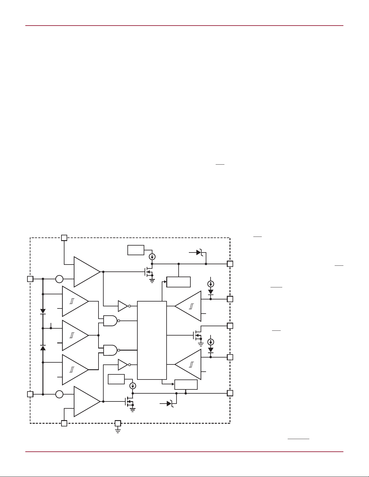
Figure 1. Functional block diagram of the LTC4224
shrinking total solution size. It does
this by combining two feature-rich and
independent Hot Swap controllers for
1V–6V applications in a 3mm × 2mm
DFN package.
Figure 1 shows a functional block
diagram of the LTC4224. The ON pin
is used to turn an external N-channel
MOSFET on or off via the GATE pin.
When commanded on, an internal
charge pump pulls the GATE above
the supply rail to fully enhance the
MOSFET, reducing its series resistance to several mΩ. The LTC4224’s
ability to derive power from the higher
of its two supplies allows it to control
load voltages as low as 1V. Active current limiting (ACL) acts on the GATE
when the load current causes more
than 25mV of voltage drop across the
sense resistor. An electronic circuit
breaker (ECB) performs the role of a
timekeeper, latching off the MOSFET
in the event of a prolonged current
overload.
Operation
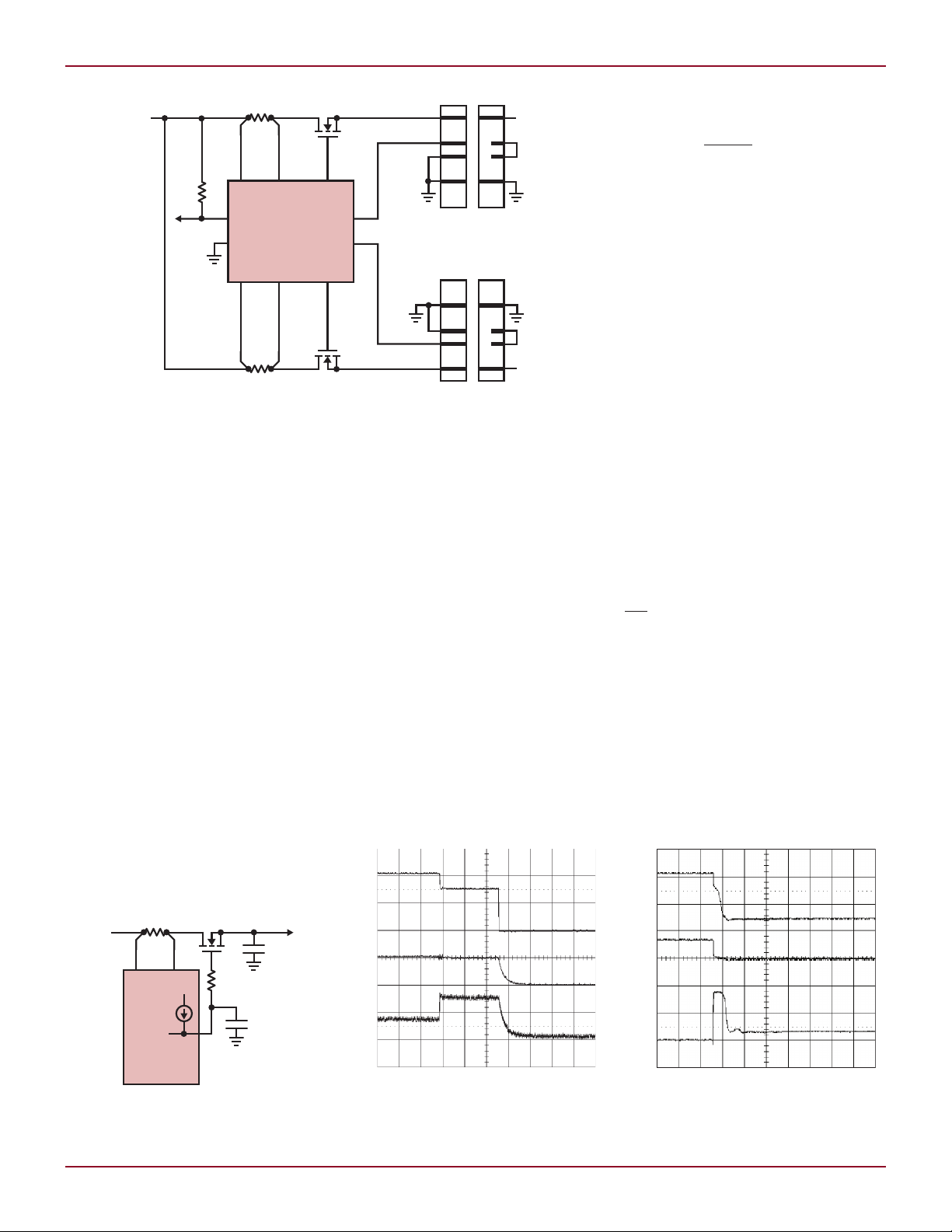
Figure 2 shows the LTC4224 together
with two N-channel MOSFETs and two
sense resistors in a 5V backplane resident Hot Swap application. Initially,
the ON pin is pulled high in the absence of an add-in card and the GATE
is held low, shutting off the MOSFET.
When an add-in card is fully inserted
into the backplane connector, the ON
pin is pulled low through the ground
connections on the card connector.
Spurious ON transitions can occur
as the connectors mate. To prevent
the MOSFET from turning on prema
turely, the LTC4224 waits out these
short term transitions with an internal
10ms debounce delay that restarts
every time ON transitions high.
To turn on the MOSFET, an internal charge pump sources 10µA to
soft-start the GATE with a slew rate
of 10µA/C
, where C
ISS
is the exter-
ISS
nal MOSFET’s gate capacitance. The
start-up inrush current flowing into
the load capacitor C
(C
OUT/CISS
) • 10µA. However, if the
is limited to
OUT
sense resistor voltage drop becomes
too large, the inrush current is limited
at 25mV/R
by the ACL. The ECB
SENSE
monitors the ACL, and if it detects that
the current limit is still active 5ms after
the GATE began ramping, the MOSFET
latches off and FAULT pulls low. If
-
21
L DESIGN FEATURES
LTC4224
V
CC1
SENSE1
SENSE2
GATE1
GATE2
GND
ON1
ON2
FAULT
V
CC2
R1
0.004Ω
R2
0.004Ω
5V
5A
5V
5A
5V
R3
10k
Q1
Si7336ADP
Q2
Si7336ADP
BACKPLANE
CONNECTOR1
CARD
CONNECTOR1
PRSNT1
PRSNT2
BACKPLANE
CONNECTOR2
CARD
CONNECTOR2
0.5µs/DIV
I
OUT2
8A/DIV
V
OUT2
5V/DIV
GATE2
5V/DIV
2ms/DIV
I
OUT1
1A/DIV
V
OUT1
5V/DIV
GATE1
5V/DIV
LTC4224
V
CC1
SENSE1
GATE1
R1
0.015Ω
5V
I
GATE
C
GATE
R
G
10Ω
C
LOAD
Q1
Figure 2. Hot Swap application for two add-in cards
C
cannot be sufficiently charged
OUT
within this period, connect a capacitor from GATE to ground to lower the
inrush current, as shown in Figure 3.
With C
duced to (C
Adjusting C
current stays below the ECB threshold
prevents ECB faults with large load
capacitors.
Overcurrent Protection
An important feature of the LTC4224
is its 25mV electronic circuit breaker
(ECB) threshold with a 10% tolerance.
This low ECB threshold allows the use
of sense resistors with lower power ratings and hence smaller packages. In
addition, the ECB threshold must not
cut excessively into the supply voltage
, the inrush current is re-
GATE
OUT
GATE
/(C
+ C
GATE
ISS
so that the inrush
)) • 10µA.
tolerance of downstream circuits. For
instance, if the downstream circuits
can tolerate at most a 5% variation on
the 1V supply, the ECB threshold of an
upstream Hot Swap controller must be
significantly lower than 50mV.
To guard against damage to the
external MOSFET from excessive
power dissipation, active current
limiting (ACL) regulates the gate to
limit the sense resistor’s voltage drop
to about 25mV. To minimize external
components, the current limit loop
is compensated by the parasitic gate
capacitance C
remains stable for C
of the MOSFET and
ISS
values as low
ISS
as 600pF. During ACL, the ECB activates and initiates an internal time-out
period of 5ms. The waveform in Figure
4 shows the LTC4224 limiting the
current and subsequently latching
off the MOSFET due to a mild current
overload at the output lasting longer
than 5ms. FAULT is pulled low; this
could either instruct the microprocessor to take actions or light an LED to
attract operator’s attention.
In the event of a severe short-circuit,
the current typically overshoots the
current limit level significantly as the
gate overdrive of the external MOSFET
is large initially. The LTC4224 responds in less than 0.1µs to swiftly
discharge the gate with a 100mA current sink. Figure 5 shows the LTC4224
bringing the current under control in
less than 0.5µs when a 3.3V rail is
shorted into a 10mΩ load without any
load capacitance. Also due to the fast
ACL is the absence of gate undershoot,
despite the speed at which the gate is
discharged. The potential peak current
is dictated by DC resistances along the
power path (trace resistance + R
the MOSFET + R
+ 10mΩ), while
SENSE
DSON
of
the path’s parasitic inductance limits
the current slew rate.
After the MOSFET latches off, the
ON pin must be pulled above 0.8V
to reset the internal fault latch. Alternatively, recycle the supply below
its UV level. The LTC4224-1 latches
off after a fault, while the LTC4224-2
automatically tries to apply power four
seconds after latching off.
Optical Transceiver
Hot Swap Application
Optical transceivers such as those
specified for the popular XENPAK/X2
Figure 3. A method to adjust inrush current
by gate capacitor. RG prevents parasitic selfoscillation in Q1
22
Figure 4. Active current limiting latches
off the external MOSFET following a mild
overcurrent
Figure 5. Fast current limit isolates severe
short circuit fault in less than 0.5µs
Linear Technology Magazine • September 2008
DESIGN FEATURES L
LTC4224
V
CC1
SENSE1 SENSE2 GATE1 GATE2
GNDGND
ON1PWREN
ON2
FAULTPWRFLT
V
CC2
R2
0.004Ω
R1
0.004Ω
5V
5A
3.3V
5A
R3
10k
Z2
R
SNUB2
10Ω
C
SNUB2
100nF
Z1
R
SNUB1
10Ω
C
SNUB1
100nF
Q2
Si7336ADP
Q1
Si7336ADP
BACKPLANE
CONNECTOR
CARD
CONNECTOR
Z1: SMAJ6.5A
Z2: SMAJ5.0A
5V
3.3V
TOP SIDE
FDS6911
BOTTOM SIDE
LTC4224
11
6
8
7
9
10
5
4
2
3
1
5
6
4
3
7
8
2
1
5V3.3V
R2 R1
LTC4224
V
CC1
SENSE1 SENSE2 GATE1
GATE2
GND
ON1
ON2FAULT
V
CC2
Q1
Q2
FDS6911
R2
0.010Ω
R1
0.015Ω
R3
390
D1
5V
BULK SUPPLY
BYPASS CAPACITOR
BULK SUPPLY
BYPASS CAPACITOR
3.3V
R
MOD_DET
1k
GND
5V
1A
3.3V
2A
CONNECTOR PLUG-IN CARD
MOD DETECT
Multi- Source Agreements (MSA) are
employed in high speed networking
routers as an interface between optical and electrical signals. The MSA
mandates hot plug capability for
transceiver modules, which are supplied with 5V, 3.3V and 1.xV.
A Hot Swap application based on
the LTC4224 for the 5V and 3.3V rails
is shown in Figure 6. Typically, a dedicated DC/DC converter controls the
1.xV rail and limits the inrush current
for each module. As the optical module
consumes relatively little power, a dual
FET such as the FDS6911 is a good
candidate for the power switches,
saving cost and minimizing area. For
the tiniest solution, sense resistors in
a 0603 case size are selected. Figure 7
shows the full solution, which fits in
the footprint of an SO8 package. In an
application where all the three supply
rails need to be hot swapped, three
LTC4224s can be used to control the
power to two modules, all in a solution
no larger than the footprint of three
SO8 packages.
3mm × 2mm DFN package. Fast
current limiting ensures that system
disturbances are minimized during
a severe overload and that faults are
Figure 6. XENPAK/X2 optical module Hot Swap application
quickly isolated. The LTC4224 offers
a complete and robust Hot Swap solution for XENPAK/X2 optical modules
that can be implemented in an SO8
footprint.
L
5V/5A, 3.3V/5A
Hot Swap Application
The LTC4224 can also reside on an
add-in card as shown in Figure 8.
There are no bulk capacitors on the
inputs as these could draw large inrush current. In their place are the
Transient Voltage Suppressors (Z1
and Z2) and RC Snubber networks.
During current transients, inductive
kickback can cause the input supply to
swing beyond the absolute maximum
(ABSMAX) rating of LTC4224’s input
pins without the TVS. By clamping the
voltage, the TVS protects the LTC4224
from damage and an ABSMAX rating
of 9V provides margin for the selection of the TVS. Snubbers damp the
parasitic LC tanks to eliminate ringing
on the input supplies. The Si7336ADP
has been chosen for its SOA, 20V
Gate-Source breakdown voltage and
low R
Conclusion
The LTC4224 simplifies the design of
low voltage Hot Swap applications by
integrating two Hot Swap controller
and timing delay circuits in a tiny
Linear Technology Magazine • September 2008
DSON
.
Figure 7. A compact PCB layout of the sense resistors, MOSFET and the LTC4224
Figure 8. A 5V and 3.3V card resident Hot Swap application
23
 Loading...