

LTC4223-1/LTC4223-2
Dual Supply Hot Swap
Controller for Advanced
Mezzanine Card
FEATURES
■
Allows Safe Insertion into Live AMC or MicroTCA
Backplane
■
Controls 12V Main and 3.3V Auxiliary Supplies
■
Limits Peak Fault Current in ≤1μs
■
Adjustable Current Limit with Circuit Breaker
■
Integrated 0.3Ω AUX Switch
■
High Side Current Sense
■
Gate Drive for External N-Channel MOSFET
■
Adjustable Response Time for Overcurrent Protection
■
Adjustable Supply Voltage Power-Up Rate
■
Thermal Shutdown Protection
■
LTC4223-1: Latch Off After Fault
■
LTC4223-2: Automatic Retry After Fault
■
16-Lead SSOP and 5mm × 4mm DFN Packages
APPLICATIONS
■
Advanced Mezzanine Card, MicroTCA Systems
■
Workstations and Server I/O
■
Telecom Networks
DESCRIPTION
The LTC®4223 positive voltage Hot SwapTM controller
allows a board to be safely inserted and removed from
a live AMC or MicroTCA backplane. It controls the main
12V supply with an external N-channel MOSFET and the
3.3V auxiliary supply with an integrated switch. The 12V
output ramp rate is adjustable and includes inrush current
limiting. The 12V output is also protected against short
circuit faults with a fast acting current limit and a 5%
accurate timed circuit breaker. The 3.3V output includes
both soft start and overcurrent protection.
The LTC4223 features a current monitor output for the
12V supply, and reports fault and power-good status for
both supplies. It also detects card presence and allows
independent control of the 12V and auxiliary 3.3V supply outputs. The LTC4223-1 features a latch-off circuit
breaker, while the LTC4223-2 provides automatic retry
after a fault.
, LT, LTC and LTM are registered trademarks of Linear Technology Corporation.
All other trademarks are the property of their respective owners.
TYPICAL APPLICATION
Advanced Mezzanine Card Application
6mΩ Si7336ADP
12V
12V
SENSE
IN
AUXIN
V
CC
AUXON
12ON
AUXPGOOD
12PGOOD
FAULT
12IMON
GND
10Ω
47Ω
12V
GATE
LTC4223-1/LTC4223-2
TIMER
0.1μF
IPMC
12V
3.3V
51Ω
330nF
ADC
15nF
12V
OUT
AUXOUT
422312 TA01a
EN
CARRIER
CONNECTOR
12V
7.4A
3.3V
150mA
MODULE
CONNECTOR
EN
5V/DIV
AUXOUT
5V/DIV
12V
OUT
5V/DIV
AUXPGOOD
5V/DIV
12PGOOD
5V/DIV
Normal Power-Up Waveform
20ms/DIV
422312 TA01b
422312f
1
LTC4223-1/LTC4223-2
ABSOLUTE MAXIMUM RATINGS
(Note 1)
Supply Voltages
12V
..................................................... –0.3V to 20V
IN
AUXIN .................................................... –0.3V to 10V
........................................................... –0.3V to 7V
V
CC
Input Voltages
⎯E⎯
12ON, AUXON,
TIMER ..........................................–0.3V to V
12V
............................................... –0.3V to 20V
SENSE
N ................................... –0.3V to 7V
+ 0.3V
CC
Output Voltages
⎯F⎯A⎯U⎯L⎯
T, ⎯1⎯2⎯P⎯G⎯O⎯O⎯D, ⎯A⎯U⎯X⎯P⎯G⎯O⎯O⎯D,
12IMON ................................................... –0.3V to 7V
PIN CONFIGURATION
12V
12V
................................................. –0.3V to 25V
GATE
OUT
- 12V
(Note 3) ................... –4.5V to 0.3V
GATE
AUXOUT ................................................. –0.3V to 10V
Operating Temperature Range
LTC4223-1C/ LTC4223-2C ....................... 0°C to 70°C
LTC4223-1I/ LTC4223-2I ..................... –40°C to 85°C
Storage Temperature Range
GN Package .......................................–65°C to 150°C
DHD Package ..................................... –65°C to 125°C
Lead Temperature (Soldering, 10sec)
GN Package ......................................................300°C
12V
12IMON
AUXON
SENSE
12V
12ON
AUXIN
V
GND
IN
CC
T
JMAX
TOP VIEW
1
2
3
4
5
6
7
8
GN PACKAGE
16-LEAD PLASTIC SSOP
= 125°C, θJA = 110°C/W
16
15
14
13
12
11
10
9
12V
GATE
12V
OUT
12PGOOD
FAULT
AUXOUT
AUXPGOOD
EN
TIMER
12V
SENSE
12V
12IMON
12ON
AUXIN
AUXON
GND
16-LEAD (5mm × 4mm) PLASTIC DFN
EXPOSED PAD (PIN 17) PCB GND CONNECTION OPTIONAL
MUST BE SOLDERED TO PCB TO OBTAIN
= 43°C/W, OTHERWISE θJA = 140°C/W, T
θ
JA
IN
V
CC
TOP VIEW
1
2
3
4
5
6
7
8
DHD PACKAGE
16
12V
GATE
15
12V
OUT
14
12PGOOD
13
12
11
10
9
FAULT
AUXOUT
AUXPGOOD
EN
TIMER
JMAX
= 125°C
17
ORDER INFORMATION
LEAD FREE FINISH TAPE AND REEL PART MARKING* PACKAGE DESCRIPTION TEMPERATURE RANGE
LTC4223CDHD-1#PBF LTC4223CDHD-1#TRPBF 42231 16-Lead (5mm × 4mm) Plastic DFN 0°C to 70°C
LTC4223CDHD-2#PBF LTC4223CDHD-2#TRPBF 42232 16-Lead (5mm × 4mm) Plastic DFN 0°C to 70°C
LTC4223IDHD-1#PBF LTC4223IDHD-1#TRPBF 42231 16-Lead (5mm × 4mm) Plastic DFN –40°C to 85°C
LTC4223IDHD-2#PBF LTC4223IDHD-2#TRPBF 42232 16-Lead (5mm × 4mm) Plastic DFN –40°C to 85°C
LTC4223CGN-1#PBF LTC4223CGN-1#TRPBF 42231 16-Lead Plastic SSOP 0°C to 70°C
LTC4223CGN-2#PBF LTC4223CGN-2#TRPBF 42232 16-Lead Plastic SSOP 0°C to 70°C
LTC4223IGN-1#PBF LTC4223IGN-1#TRPBF 4223I1 16-Lead Plastic SSOP –40°C to 85°C
LTC4223IGN-2#PBF LTC4223IGN-2#TRPBF 4223I2 16-Lead Plastic SSOP –40°C to 85°C
Consult LTC Marketing for parts specifi ed with wider operating temperature ranges. *The temperature grade is identifi ed by a label on the shipping container.
Consult LTC Marketing for information on non-standard lead based fi nish parts.
For more information on lead free part marking, go to: http://www.linear.com/leadfree/
For more information on tape and reel specifi cations, go to: http://www.linear.com/tapeandreel/
2
422312f
LTC4223-1/LTC4223-2
ELECTRICAL CHARACTERISTICS
The ● denotes the specifi cations which apply over the full operating
temperature range, otherwise specifi cations are T
= 25°C, VCC = 3.3V, V
A
SYMBOL PARAMETER CONDITIONS MIN TYP MAX UNITS
Supplies
V
DD
Input Supply Range V
CC
AUXIN
12V
IN
I
DD
Input Supply Current V
CC
AUXIN
12V
IN
V
DD(UVLO)
ΔV
DD(UVLO,
HYST)
Input Supply Undervoltage Lockout VCC Rising
V
Rising
AUXIN
V
Rising
12VIN
Input Supply Undervoltage Lockout
Hysteresis
V
CC
AUXIN
12V
IN
Current Limit
ΔV
SENSE(CB)
ΔV
SENSE(ACL)
I
AUX(ACL)
Circuit Breaker Trip Sense Voltage,
(V
12VIN
– V
12VSENSE
)
Active Current Limit Sense Voltage,
(V
12VIN
– V
12VSENSE
)
AUXOUT Active Current Limit V
AUXOUT
= 0V
Integrated Switch
R
DS(ON)
Switch Resistance
(V
– V
AUXIN
AUXOUT
)/I
AUXOUT
I
= 150mA (Note 4)
AUXOUT
Gate Drive
ΔV
GATE
I
GATE(UP)
I
GATE(DN)
I
GATE(FPD)
External N-Channel Gate Drive
(V
12VGATE
– V
12VOUT
)
(Note 3)
External N-Channel Gate Pull-Up Current Gate Drive On, V
External N-Channel Gate Pull-Down Current Gate Drive Off
V
= 17V, V
12VGATE
External N-Channel Gate Fast Pull-Down
Current
Fast Turn Off
V
= 17V, V
12VGATE
Current Sense
G
12IMON
V
12IMON
ΔV
SENSE(MAX)
V
12IMON(CLP)
R
12IMON
V
12IMON(MIN)
12IMON Pin Gain Ratio
ΔV
12IMON
/Δ(V
12VIN
– V
12VSENSE
)
(V
12IMON Pin Output Voltage (V
12IMON Pin Maximum Input Sense Voltage
12IMON Pin Clamp Voltage (V
12IMON Pin Output Resistance (V
12IMON Pin Minimum Output Voltage (V
12VIN
12VIN
12VIN
12VIN
12VIN
– V
– V
– V
– V
– V
12VSENSE
12VSENSE
12VSENSE
12VSENSE
12VSENSE
Comparator Inputs
V
PG(TH)
V
PG(HYST)
V
TMR(TH)
Power Good Threshold Voltage V
Power Good Hysteresis V
TIMER Pin Threshold Voltage V
12VOUT
V
AUXOUT
12VOUT
V
AUXOUT
TIMER
V
TIMER
Falling
Falling
Rising
Falling
= 3.3V, V
AUXIN
= 0V
12VGATE
= 12V
12VOUT
= 12V
12VOUT
) = (75mV, 25mV)
) = 75mV, VCC = 2.7V
) = 150mV, VCC = 2.7V
) = 0V
) = 0V
=12V, unless otherwise specifi ed. (Note 2)
12VIN
●
2.7
●
2.7
●
10
●
●
●
●
2.3
●
2.4
●
9.4
●
40
●
70
●
70
●
47.5 50 52.5 mV
●
54 60 66 mV
●
165 240 330 mA
●
●
4.5 6.2 7.9 V
●
–7 –10 –14 μA
●
0.5 1 2 mA
●
90 160 250 mA
●
30 33 36 V/V
●
2.25 2.475 2.7 V
●
82.5 mV
●
2.9 3.2 3.5 V
●
115 165 215 kΩ
●
●
10
●
2.8
●
20
●
5
●
1.198
●
0.15
0.8
0.4
0.6
2.45
2.5
9.7
110
110
110
0.3 0.5
0 130 mV
10.3
2.885
60
16
1.235
0.2
6
6
14
2
1
1
2.6
2.6
10
180
150
150
10.6
2.97
110
30
1.272
0.25
mA
mA
mA
mV
mV
mV
mV
mV
V
V
V
V
V
V
Ω
V
V
V
V
422312f
3

LTC4223-1/LTC4223-2
ELECTRICAL CHARACTERISTICS
The ● denotes the specifi cations which apply over the full operating
temperature range, otherwise specifi cations are TA = 25°C, VCC = 3.3V, V
SYMBOL PARAMETER CONDITIONS MIN TYP MAX UNITS
I
TMR(UP)
I
TMR(DN)
TIMER Pull-Up Current V
TIMER Pull-Down Current V
Open Drain Outputs
V
OL
V
OH
I
PU
Output Low Voltage (⎯F⎯A⎯U⎯L⎯T, ⎯1⎯2⎯P⎯G⎯O⎯O⎯D,
⎯A⎯U⎯X⎯P⎯G⎯O⎯O⎯
D)
Output High Voltage (⎯F⎯A⎯U⎯L⎯T, ⎯1⎯2⎯P⎯G⎯O⎯O⎯D,
⎯A⎯U⎯X⎯P⎯G⎯O⎯O⎯
D)
Output Pin Pull-Up Current (⎯F⎯A⎯U⎯L⎯T,
⎯1⎯2⎯P⎯G⎯O⎯O⎯
D, ⎯A⎯U⎯X⎯P⎯G⎯O⎯O⎯D)
Logic Inputs
V
IN(TH)
I
IN(LEAK)
R
PU
Logic Input Threshold (12ON, AUXON, ⎯E⎯N)
Input Leakage Current (12ON, AUXON) VIN = V
⎯E⎯
N Pin Pull-Up Resistance
Other Pin Functions
I
12VSENSE
I
12VOUT
R
OUT(DIS)
12V
12V
OUT Pin Discharge Resistance
12V
Pin Input Current V
SENSE
Pin Input Current Gate Drive On, V
OUT
OUT
AUXOUT
Propagation Delays
t
CB
t
PHL(SENSE)
t
PHH(AUXON)
t
PHH(12ON)
t
RST(ON)
t
RST(VCC)
t
PLL(UVLO)
t
PHL(GATE)
t
PLH(PG)
t
P(12IMON)
AUX Circuit Breaker Trip Delay After Power Up
Sense Voltage, (12VIN – 12V
High to 12V
GATE
Low
SENSE
)
AUXON High to AUXOUT High
12ON High to 12V
GATE
High
Input Low (12ON, AUXON) to ⎯F⎯A⎯U⎯L⎯T High
VCC Low to ⎯F⎯A⎯U⎯L⎯T High
12VIN Low to 12V
AUXIN Low to
⎯E⎯
N High to 12V
12V
Low to ⎯1⎯2⎯P⎯G⎯O⎯O⎯D High
OUT
AUXOUT Low to
Low
GATE
⎯A⎯U⎯X⎯P⎯G⎯O⎯O⎯
Low
GATE
⎯A⎯U⎯X⎯P⎯G⎯O⎯O⎯
D High
D High
Input Sense Voltage Step to 12IMON
Propagation Delay
Note 1: Stresses beyond those listed under Absolute Maximum Ratings
may cause permanent damage to the device. Exposure to any Absolute
Maximum Rating condition for extended periods may affect device
reliability and lifetime.
Note 2: All currents into device pins are positive; all currents out of
the device pins are negative. All voltages are referenced to GND unless
otherwise specifi ed.
= 1V, Initial Timing Cycle
TIMER
V
= 0V, In AUX Fault Mode
TIMER
V
= 0V, In 12V Fault Mode
TIMER
= 2V, No Faults
TIMER
V
= 2V, In Reset Mode
TIMER
= 3mA
I
OL
(Note 5)
= 1.5V
V
PU
CC
= 12V
12VSENSE
Gate Drive Off
= 6V
V
12VOUT
V
ΔV
ΔV
ΔV
AUXVOUT
SENSE
SENSE
SENSE
= 2V
= 300mV, C
= 100mV, C
= 100mV
= 3.3V, V
AUXIN
= 12V
12VOUT
= 10nF
12VGATE
= 10nF
12VGATE
Note 3: An internal clamp limits the 12V
above 12V
. Driving this pin to voltages beyond the clamp may damage
OUT
=12V, unless otherwise specifi ed. (Note 2)
12VIN
●
–7
●
–7
●
–140
●
1.3
●
2
●
●
VCC – 1 V
●
–6 –10 –14 μA
●
0.8 2 V
●
●
60 100 140 kΩ
●
10 50 100 μA
●
20 50 100 μA
●
400
●
375
●
12 25 50 μs
●
●
●
●
●
●
●
61218 μs
●
61218 μs
●
●
●
●
–10
–10
–200
2
8
–13
–13
–260
2.6
16
0.15 0.4 V
±1 μA
800
750
0.5
1600
1500
1
5
12
15 30 μs
30 60 μs
20 40 μs
80 150 μs
20 40 μs
20 40 μs
20 40 μs
26 μs
pin to a minimum of 4.5V
GATE
the device.
Note 4: For the DFN package, the AUX switch on resistance, R
DS(ON)
is guaranteed by correlation to wafer test measurements.
Note 5: The output pins
pull-up to V
of 10μA. However, an external pull-up resistor may be used
CC
when faster rise time is required or for V
⎯F⎯A⎯U⎯L⎯
T, ⎯1⎯2⎯P⎯G⎯O⎯O⎯D and ⎯A⎯U⎯X⎯P⎯G⎯O⎯O⎯D have an internal
voltages greater than VCC.
OH
μA
μA
μA
μA
mA
limit
422312f
Ω
Ω
μs
μs
4
LTC4223-1/LTC4223-2
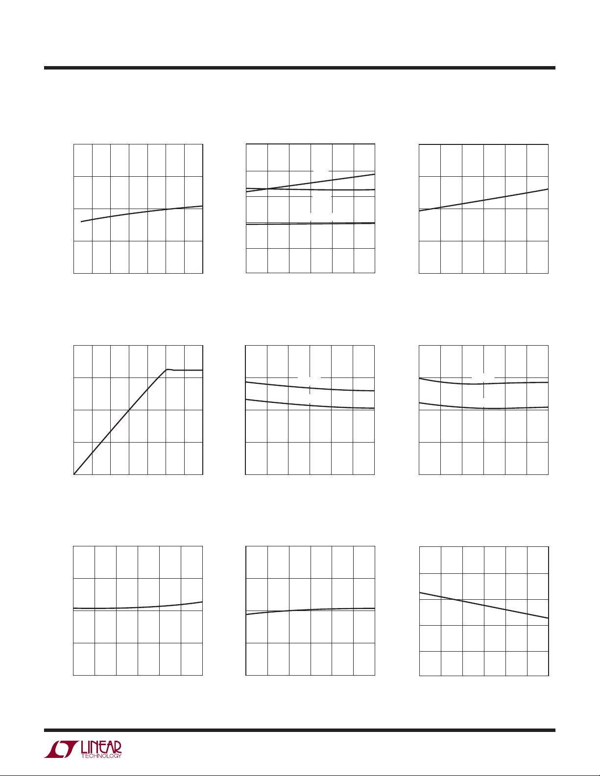
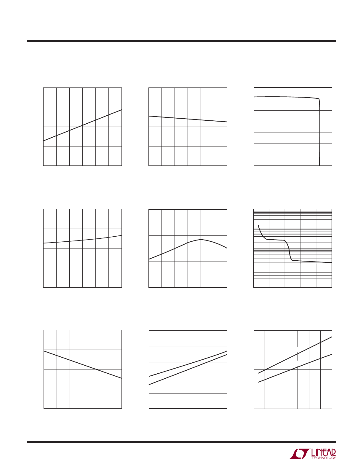
TYPICAL PERFORMANCE CHARACTERISTICS
Specifi cations are T
3.3V, V
=12V, unless otherwise specifi ed.
12VIN
ICC vs V
1.6
CC
Supply Current vs Temperature
1.0
12IMON Gain Ratio vs
Temperature
35
= 25°C, VCC = 3.3V, V
A
AUXIN
=
1.2
0.8
(mA)
CC
I
0.4
0
3.0 3.5 4.0 4.5
2.5
VCC (V)
5.0 5.5 6.0
12IMON Output Voltage vs Sense
Voltage
4
3
2
1
12IMON OUTPUT VOLTAGE (V)
0
20 40 60 80
0
SENSE VOLTAGE (mV)
100 120 140
422312 G01
422312 G04
0.8
0.6
0.4
SUPPLY CURRENT (mA)
0.2
0
–50
–25
TEMPERATURE (°C)
Power-Good Threshold vs
12V
OUT
Temperature
10.4
10.3
10.2
10.1
POWER-GOOD THRESHOLD (V)
OUT
12V
10.0
–50
–25 0 25 50 75 100
TEMPERATURE (°C)
V
CC
12V
IN
AUXIN
02550
RISING
FALLING
75 100
422312 G02
422312 G05
34
33
32
12IMON GAIN RATIO (V/V)
31
–50
–25 0 25 50 70 100
TEMPERATURE (°C)
AUXOUT Power-Good Threshold
vs Temperature
2.92
2.90
2.88
2.86
AUXOUT POWER-GOOD THRESHOLD (V)
2.84
–50
–25 0 25 50 75 100
RISING
FALLING
TEMPERATURE (°C)
422312 G03
422312 G06
Circuit Breaker Trip Voltage vs
Temperature
52
51
50
49
CIRCUIT BREAKER TRIP VOLTAGE (mV)
48
–50
–25 0 25 50 75 100
TEMPERATURE (°C)
422312 G07
Active Current Limit Sense
Voltage vs Temperature
62
61
60
59
ACTIVE CURRENT LIMIT SENSE VOLTAGE (mV)
58
–50
–25 0 25 50 75 100
TEMPERATURE (°C)
422312 G08
AUX Active Current Limit vs
Temperature
250
240
230
220
210
AUX ACTIVE CURRENT LIMIT (mA)
200
–50
02550
–25
TEMPERATURE (°C)
75 100
422312 G09
422312f
5
LTC4223-1/LTC4223-2
TYPICAL PERFORMANCE CHARACTERISTICS
Specifi cations are TA = 25°C, VCC = 3.3V, V
3.3V, V
0.5
0.4
0.3
=12V, unless otherwise specifi ed.
12VIN
AUX Switch On Resistance vs
Temperature Gate Drive vs Temperature Gate Drive vs I
) (V)
GATE
6.3
6.2
6.1
) (V)
GATE
7
6
5
4
3
GATE
AUXIN
=
0.2
AUX SWITCH-ON RESISTANCE (Ω)
0.1
–50
–25 0 25 50 75 100
TEMPERATURE (°C)
Gate Pull-Up Current vs
Temperature
–11.0
–10.5
–10.0
–9.5
GATE PULL-UP CURRENT (µA)
–9.0
–50
–25 0 25 50 75 100
TEMPERATURE (°C)
422312 G10
422312 G13
6.0
GATE DRIVE (ΔV
5.9
–50
–25 0 25 50 75 100
TEMPERATURE (°C)
AUX Circuit Breaker Trip Delay vs
Temperature
30
25
20
AUX CIRCUIT BREAKER TRIP DELAY (µs)
15
–50
02550
–25
TEMPERATURE (°C)
422312 G11
75 100
422312 G14
2
GATE DRIVE (ΔV
1
0
0
–2 –4
–6 –10
I
(μA)
GATE
Active Current Limit Delay vs
Sense Voltage
100
10
1
0.1
ACTIVE CURRENT LIMIT DELAY (µs)
0.01
50 150 200 250
100
SENSE VOLTAGE (mV)
–8 –12
422312 G12
300
422312 G15
Gate Fast Pull-Down Current vs
Temperature
250
200
150
100
GATE FAST PULL-DOWN CURRENT (mA)
50
–50
–25 0 25 50 75 100
TEMPERATURE (°C)
6
422312 G16
Output Discharge Resistance vs
Temperature Logic Input Threshold vs V
OUTPUT DISCHARGE RESISTANCE (Ω)
1200
1000
800
600
400
200
–50
02550
–25
TEMPERATURE (°C)
12V
OUT
AUXOUT
75 100
422312 G17
3.0
2.5
2.0
1.5
1.0
LOGIC INPUT THRESHOLD (V)
0.5
0
2.5
3.0 3.5
4.0 5.0
VCC (V)
CC
HIGH
LOW
4.5 5.5 6.0
422312 G18
422312f

PIN FUNCTIONS
LTC4223-1/LTC4223-2
12V
(Pin 1): 12V Current Sense Input. Connect this
SENSE
pin to the output of the current sense resistor. The electronic
circuit breaker trips if the voltage across the sense resistor
exceeds 50mV for more than a fault fi lter delay.
(Pin 2): 12V Supply Input. Undervoltage lockout
12V
IN
disables the 12V supply until the input at 12V
exceeds
IN
9.7V.
12IMON (Pin 3): 12V Current Sense Monitoring Output.
This pin monitors the sense voltage between 12V
12V
. The gain ratio between this pin’s voltage and
SENSE
IN
and
the sense voltage is 33.
12ON (Pin 4): 12V Supply On Control Digital Input. A ris-
⎯E⎯
ing edge turns on the external N-channel MOSFET if
N
is pulled low and a falling edge turns it off. A high-to-low
transition on this pin will clear the 12V supply faults.
AUXIN (Pin 5): Auxiliary Supply Input. An internal 0.3Ω
switch is connected between AUXIN and AUXOUT pins.
Undervoltage lockout holds the switch off until the input
at AUXIN exceeds 2.5V.
(Pin 6): Bias Supply Input. This pin provides power
V
CC
to the device’s internal circuitry and operates from 2.7V to
6V. Undervoltage lockout circuit disables the device until
the input at V
exceeds 2.45V. Bypass with 330nF.
CC
AUXON (Pin 7): Auxiliary Supply On Control Digital Input.
⎯E⎯
A rising edge turns on the internal switch if
N is pulled
low and a falling edge turns it off. A high-to-low transition on both this pin and 12ON pin will clear the auxiliary
supply faults.
GND (Pin 8): Device Ground.
TIMER (Pin 9): Timer Capacitor Terminal. Connect a
capacitor between this pin and ground to set a 741ms/μF
duration for initial timing cycle, 123ms/μF for AUX current
limit during power-up and 6ms/μF duration for 12V current
limit before the external MOSFET is turned off.
⎯E⎯
N (Pin 10): Enable Input Intended for Card Presence
Detect. Ground this pin to enable the external N-channel
MOSFET and internal switch to turn on. If this pin is pulled
high, the switches are not allowed to turn on. An internal
100k resistor pulls up this pin. A high-to-low transition
will clear faults.
⎯A⎯U⎯X⎯P⎯G⎯O⎯O⎯
D (Pin 11): Auxiliary Supply Power Status
Output. Open drain output that is normally pulled high
by an internal 10μA current source or an external pull-up
resistor to V
. It pulls low when the AUXOUT pin voltage
CC
exceeds the power-good threshold of 2.901V.
AUXOUT (Pin 12): Auxiliary Supply Output. This pin is
the output from the internal switch connected between
AUXIN and AUXOUT pins. It signals
⎯A⎯U⎯X⎯P⎯G⎯O⎯O⎯
D low when
it exceeds 2.901V. A 750Ω active pull-down discharges
AUXOUT to ground when the internal switch is turned
off.
⎯F⎯A⎯U⎯L⎯
T (Pin 13): Auxiliary and 12V Supply Fault Status
Output. Open drain output that is normally pulled high by an
internal 10μA current source or an external pull-up resistor
. It pulls low when the circuit breaker is tripped due
to V
CC
to an overcurrent fault on auxiliary or 12V supply.
⎯1⎯2⎯P⎯G⎯O⎯O⎯
D (Pin 14): 12V Supply Power Status Output.
Open drain output that is normally pulled high by an internal 10μA current source or an external pull-up resistor
. It pulls low when the 12V
to V
CC
pin voltage exceeds
OUT
the power-good threshold of 10.36V.
12V
(Pin 15): 12V Gate Drive Return and Power-Good
OUT
Input. Connect this pin to the source of the external Nchannel MOSFET for gate drive return. This pin signals
⎯1⎯2⎯P⎯G⎯O⎯O⎯
MOSFET is turned off, 12V
D low when it exceeds 10.36V. When the external
is discharged to ground
OUT
through a 800Ω active pull-down.
12V
(Pin 16): Gate Drive for 12V Supply External N-
GATE
Channel MOSFET. An internal 10μA current source charges
the gate of the external N-channel MOSFET. An internal
clamp limits the gate voltage to 6.2V above 12V
OUT
. A
resistor and capacitor network from this pin to ground
sets the turn-on rate and compensates the active current
limit. During turn-off, a 1mA pull-down current discharges
12V
lockout, a 160mA pull-down current between 12V
12V
to ground. During short circuit or undervoltage
GATE
is activated.
OUT
GATE
and
Exposed Pad (Pin 17, DHD Package): Exposed pad may
be left open or connected to device ground.
422312f
7
LTC4223-1/LTC4223-2
FUNCTIONAL DIAGRAM
CHARGE
PUMP
12V
IN
12V
SENSE
12ON 12V FET ON
60mV
+
50mV
+
–
–
R
IN
5k
10μA
ACL
+
–
ECB
+
1mA
A1
+
–
R
OUT
165k
6.2V
GATE
DRIVER
12IMON
12V
GATE
12V
OUT
–
10μA
PG2
+
10.3V
–
12PGOOD
12V SUPPLY
CONTROL
12V PWRGD
V
CC
V
CC
2μA
R2
UVLO3
+
12V
IN
9.7V
–
UVLO2
+
2.45V
VCCV
CC
10μA
AUXIN
2.5V
0.2V
–
+
–
+
UVLO1
CP2
–
CP1
+
1.235V
–
EN CARD PRESENCE
V
CC
200μA
TIMER
AUXON AUX FET ON
GND
SYSTEM
CONTROL
AUX SUPPLY
CONTROL
12V FAULT
AUX FAULT
V
CC
10μA
FAULT
V
CC
10μA
AUXPGOOD
8
AUXIN
THERMAL
SHUTDOWN
MFETRSNS
AUX PWRGD
10μA
PG1
CHARGE
PUMP
+
2.885V
–
AUXOUT
422312 FD
422312f

OPERATION
LTC4223-1/LTC4223-2
The LTC4223 is designed to control the power on an Advanced Mezzanine Card (AMC) or MicroTCA backplane,
allowing boards to be safely inserted and removed. It
controls the 12V main and 3.3V auxiliary power through an
external N-channel MOSFET and integrated pass transistor.
These two supplies can be turned on and off independently
by their respective ON control pins.
If either AUXON or 12ON is pulled high, an initial timing cycle set by the TIMER capacitor value is initiated
once all these conditions are met: input supplies out of
⎯E⎯
undervoltage lockout; TIMER < 0.2V and
end of the initial timing cycle, if the AUXON pin is high, the
internal pass transistor turns on. It enters into an active
current limit loop if the inrush current charging the load
capacitor exceeds 240mA. When the load is in current
limit, a 10μA pull-up charges the TIMER pin capacitor. If
the load capacitor is fully charged and the switch is no
longer in current limit before the TIMER reaches 1.235V,
⎯A⎯U⎯X⎯P⎯G⎯O⎯O⎯
Otherwise the internal switch turns off and
low when TIMER reaches 1.235V.
If 12ON pin is high at the end of the initial timing cycle,
an internal charge pump charges the gate of the external
MOSFET with 10μA pull-up. Connecting an external gate
capacitor limits the inrush current charging the load capacitor. If the inrush current exceeds its limited current
D pulls low indicating that power is good.
N low. At the
⎯F⎯A⎯U⎯L⎯
T pulls
value, an internal analog current limit (ACL) amplifi er
servos the gate to force 60mV across the external sense
resistor connected between 12VIN and 12V
During this period, TIMER pin capacitor is charged by a
200μA pull-up. If the load is fully charged and no longer in
current limit before the TIMER reaches 1.235V,
pulls low. Otherwise 12V shuts off and
when TIMER reaches 1.235V.
If an overcurrent fault occurs on the auxiliary supply after
power-up, the current is limited to 240mA and after a 25μs
delay, the circuit breaker trips and
mal shutdown protects the internal pass transistor from
overheating by shutting it off at 150°C. If an overcurrent
fault occurs on the 12V supply, the current is limited to
60mV/R
charging the TIMER capacitor, the circuit breaker trips
⎯F⎯A⎯U⎯L⎯
and
supply shuts off 12V; a fault on the 12V supply does not
affect the auxiliary supply.
The LTC4223 provides high side current sensing information for the 12V supply at the 12IMON pin. The 12IMON
output voltage is 33 times the sense voltage, allowing it
to be used with an external ADC.
In the off condition, 12V
to ground by internal N-channel pull downs.
. After a timing cycle delay set by 200μA
SENSE
T pulls low. An overcurrent fault on the auxiliary
and AUXOUT are discharged
OUT
⎯F⎯A⎯U⎯L⎯
⎯F⎯A⎯U⎯L⎯
T pulls low. Ther-
pins.
SENSE
⎯1⎯2⎯P⎯G⎯O⎯O⎯
T pulls low
D
422312f
9

LTC4223-1/LTC4223-2
APPLICATIONS INFORMATION
INTELLIGENT
PLATFORM
MANAGEMENT
CONTROLLER
MP ENABLE
PWR ENABLE
MP GOOD
PWR GOOD
FAULT
3
3.3V
2.2k
PRESENCE
12V
BULK SUPPLY
BYPASS CAPACITOR
3.3V
BULK SUPPLY
BYPASS CAPACITOR
3.3V 3.3V 3.3V
V
7
CLK
6
D
OUT
1
CS
R5*
R6*
10k
10k
58
V
REF
CC
LTC1197L
GND
4
+IN
–IN
1μF
R2
51Ω
R4*
10k
2
3
C2
330nF
3.3V
R
S
6mΩ
21 16
12V
5
6
7
4
11
14
13
3
12V
AUXIN
V
CC
AUXON
12ON
AUXPGOOD
12PGOOD
FAULT
12IMON
SENSE
IN
GND
89
Q1
Si7336ADP
R3
10Ω
12V
GATE
LTC4223-1
TIMER
R
47Ω
C
T
0.1μF
G
C
G
15nF
12V
AUXOUT
422312 F01
OUT
EN
CARRIER AMC
CONNECTOR
PWR
15
12
MP
10
PS1
PS0
MODULE AMC
CONNECTOR
12V
7.4A
3.3V
150mA
3.3V
RESET
*OPTIONAL
Figure 1. Advanced Mezzanine Card/MicroTCA Application
The typical LTC4223 application is in a Carrier board
for Advanced Mezzanine Cards (AMC), delivering 3.3V
auxiliary and 12V power to the AMC module. A controller on the Carrier board sequences the turn-on of power
supplies and manages the fault and power-good reports
from the LTC4223.
The LTC4223 detects board presence during insertion and
extraction, allowing power to be delivered in a controlled
manner without damaging the connector. The typical
LTC4223 application circuit is shown in Figure 1. External
component selection is discussed in detail in the Design
Example section.
10
ENABLE
10k
Turn-On Sequence
The power supplies delivered to an AMC module are
controlled by the external N-channel pass transistor, Q1 in
the 12V power path and an internal pass transistor in the
3.3V auxiliary power path. Sense resistor R
monitors the
S
12V load current for fault detection and current sensing
information. GATE capacitor C
control to limit the inrush current. Resistor R
provides gate slew rate
G
with CG
G
compensates the current control loop while R3 prevents
parasitic oscillations in Q1.
422312f

APPLICATIONS INFORMATION
LTC4223-1/LTC4223-2
Several conditions must be met before the external and
internal switches are allowed to turn on. First V
the input supplies (12V
, AUXIN) must exceed their
IN
CC
and
undervoltage lockout thresholds. Next TIMER must be
⎯E⎯
<0.2V and
N must be pulled low.
Once these conditions are met, a debounce timing cycle is
initiated when AUXON or 12ON pin is toggled from low to
high. These two control pins turn on/off the 3.3V auxiliary
and 12V supplies. At the end of the debounce cycle, the
ON pins and fault status are checked. If both ON pins are
high and fault is cleared, the 3.3V auxiliary supply starts
up fi rst followed by the 12V supply. Note that the turn-on
delay for the AUXON and 12ON pins is 15μs and 30μs.
Figure 2 shows the two supplies turning on in sequence
⎯E⎯
N goes low.
after
By default, the internal pass transistor turns on fi rst if
both ON pins are high and start-up conditions met. The
output is current limited at 240mA by its internal ACL
amplifi er as the load current charging the output capacitor increases. This causes the TIMER to ramp up with a
10μA pull-up. Normally the AUXOUT voltage exceeds its
power-good threshold before TIMER time-out and then
⎯A⎯U⎯X⎯P⎯G⎯O⎯O⎯
D pulls low.
EN
5V/DIV
TIMER
2V/DIV
AUXOUT
5V/DIV
12V
OUT
5V/DIV
AUXPGOOD
5V/DIV
12PGOOD
5V/DIV
20ms/DIV
Figure 2. Normal Power-Up Sequence
422312 F02
Once AUXOUT signals power is good and the TIMER pin
returns to <0.2V, the external MOSFET is then allowed to
turn on by charging up the GATE with a 10μA current source
(Figure 2). The voltage at the GATE pin rises with a slope
equal to 10μA/C
into the load capacitor C
I
INRUSH
=
and the supply inrush current fl owing
G
(see Figure 14) is limited to:
L1
C
1
L
µA
10•
C
G
The 12V output follows the GATE voltage when the MOSFET
turns on. If the voltage across the current sense resistor
becomes too high, the inrush current is limited by the
R
S
internal current limit circuitry. Once the output, 12V
exceeds its power-good threshold,
⎯1⎯2⎯P⎯G⎯O⎯O⎯
D also pulls
OUT
low.
If only the 12ON pin is high at the end of debounce cycle,
the external MOSFET turns on fi rst. After that, if AUXON
pulls high, the internal switch turns on only after the 12V
output signals power is good and TIMER <0.2V.
Table 1. 12V and Auxiliary Supply Turn-Off Conditions
CONDITION RESULT CLEARED BY
AUX 12V
AUXON Goes
Low
12ON Goes Low No Effect Turns Off 12ON High
⎯E⎯
N Goes High Turns Off Turns Off⎯E⎯N Low
UVLO on V
UVLO on AUXIN Turns Off No Effect AUXIN > UVLO
UVLO on 12V
AUX Overcurrent
Fault
12V Overcurrent
Fault
Thermal
Shutdown
CC
Turns Off No Effect AUXON High
Turns Off Turns Off VCC > UVLO
No Effect Turns Off 12VIN > UVLO
IN
Turns Off Turns Off AUXON and 12ON Low,
No Effect Turns Off 12ON Low, ⎯E⎯N High-to-
Turns Off Turns Off AUXON and 12ON Low,
⎯E⎯
N High-to-Low, UVLO
on V
CC
Low, UVLO on V
⎯E⎯
N High-to-Low, UVLO
on V
CC
120°C
CC
, Temperature <
422312f
11

LTC4223-1/LTC4223-2
APPLICATIONS INFORMATION
Turn-Off Sequence
The switches can be turned off by various conditions and
this is summarized in Table 1.
When the 12ON pin goes low, the external switch is turned
off with the GATE pin pulled to ground by 1mA current
sink. The
⎯1⎯2⎯P⎯G⎯O⎯O⎯
D pin pulls high indicating that power is
no longer good, while an internal N-channel transistor discharges the output to ground. Similarly, when the AUXON
pin goes low, the internal switch is turned off,
⎯A⎯U⎯X⎯P⎯G⎯O⎯O⎯
D
pulls high while its output is discharged to ground through
an internal N-channel transistor. Figure 3 shows the two
⎯E⎯
supplies being turned off by
N going high.
Card Presence Detect
⎯P⎯S⎯
In an AMC system,
1 and ⎯P⎯S⎯0 signals are used to
detect the presence of a card upon insertion or removal.
⎯P⎯S⎯
Normally
resistor. If AUXON or 12ON is high when the
1 is connected to the ⎯E⎯N pin with a pull-up
⎯E⎯
N pin goes
low, indicating a board insertion, a timing cycle for contact
debouncing is initiated. Upon insertion, any bounces on the
⎯E⎯
N pin will re-start the timing cycle. When TIMER fi nally
reaches its threshold during ramp up, the fault latches
⎯E⎯
will be cleared. If the
N pin remains low at the end of the
timing cycle, the switches are allowed to turn on.
⎯E⎯
If the
N pin is toggled from low to high, indicating board
removal, all the switches will be turned off after a 20μs delay.
Any latched faults will not be cleared. However, removing
⎯E⎯
the card could cause the
N pin voltage to bounce, clearing
the fault latches undesirably. This is prevented by blanking
the bounces internally with a TIMER ramp up period given
• 123[ms/μF] as shown in Figure 4.
by C
T
Timer Functions
An external capacitor C
connected from the TIMER pin
T
to ground is used to perform several functions.
1. Ignore contact debouncing during card insertion when
the device is enabled. The debounce cycle is given
by ramping up C
with 10μA current to TIMER high
T
threshold (1.235V) and then ramping down with 2μA
current to below TIMER low threshold (0.2V). This gives
an average debounce cycle time of C
After that, if any ON pin is pulled high and
• 741[ms/μF].
T
⎯E⎯
N pin is
low, the switches can be turned on.
⎯E⎯
2. Blanking contact bounce on the
N pin that might
trigger unwanted fault clearing during card removal.
The blanking time is given by C
• 123[ms/μF].
T
3. Fault fi ltering during auxiliary supply power-up in analog
current limit. TIMER pulls up with 10μA and pulls down
with 2μA. The fi lter time is given by C
• 123[ms/μF].
T
4. 12V supply fault fi ltering during and after power-up
in analog current limit. TIMER pulls up with 200μA
and pulls down with 2μA. The fi lter time is given by
• 6[ms/μF].
C
T
5. For cooling off during an auto-retry cycle after
an overcurrent fault on auxiliary or 12V supply
(LTC4223-2). The cool-off time is given by C
[ms/μF] after an auxiliary supply fault and C
• 1482
T
• 1358[ms/
T
μF] after a 12V supply fault.
12
EN
5V/DIV
AUXOUT
5V/DIV
12V
OUT
5V/DIV
AUXPGOOD
5V/DIV
12PGOOD
5V/DIV
100ms/DIV
Figure 3. Normal Power-Down Sequence Figure 4. Debouncing by TIMER during Card Removal
422312 F03
2V/DIV
TIMER
1V/DIV
FAULT
2V/DIV
EN
5ms/DIV
422312 F04
422312f

APPLICATIONS INFORMATION
LTC4223-1/LTC4223-2
As the TIMER capacitor is used for fault fi ltering during
power-up for both the auxiliary and 12V supplies, only
one supply can be started up at any one time. The other
supply waits until the power-good signal is generated by
the powering-up supply and the TIMER pin voltage falls
below 0.2V. By default, the 3.3V auxiliary supply starts up
fi rst if both AUXON and 12ON are high at the end of the
debounce cycle.
Whenever both AUXON and 12ON are pulled low, the device is in reset mode and TIMER capacitor is discharged
to ground by an 8mA current sink.
Thermal Shutdown
The internal 3.3V auxiliary supply switch is protected by
thermal shutdown. If the switch’s temperature reaches
⎯F⎯A⎯U⎯L⎯
150°C, the aux switch will shut off immediately and
T
will pull low. The external 12V supply switch also turns
off. The switches are allowed to turn on again by cycling
both the AUXON and 12ON pins low then high after the
internal switch’s temperature falls below 120°C.
Overcurrent Fault
The LTC4223 features an adjustable current limit with circuit
breaker function that protects the external MOSFET against
FAULT
5V/DIV
I
LOAD
5A/DIV
12V
OUT
5V/DIV
12V
GATE
5V/DIV
0.1ms/DIV
Figure 5. Overcurrent Fault on 12V Output
422312 F05
short circuits or excessive load current on 12V supply. The
voltage across the external sense resistor is monitored by
the analog current limit (ACL) amplifi er and the electronic
circuit breaker (ECB) comparator. If an overcurrent fault
occurs that causes the sense voltage to reach the ACL
threshold (60mV), the ACL amplifi er regulates the MOSFET
to prevent any further increase in current. This overcurrent
condition results in a sense voltage that exceeds the ECB
threshold. As a result, the TIMER capacitor is charged
by a 200μA current. If the condition persists, the TIMER
pin voltage will reach its threshold (1.235V). When this
⎯F⎯A⎯U⎯L⎯
occurs, the
T pin pulls low and a 1mA current pulls
the GATE pin to ground causing the MOSFET to turn off.
The circuit breaker time delay, the time required for the
TIMER pin capacitor to charge from ground to the TIMER
pin threshold, is given by C
• 6[ms/μF].
T
After the MOSFET turns off, the TIMER pin capacitor discharges with a 2μA pull-down current. For the auto-retry
version (LTC4223-2), if the TIMER discharges to below
0.2V, a new start-up cycle will begin. The TIMER starts
ramping up and clears faults when it exceeds 1.235V;
thereafter it ramps down (see the section on Auto-Retry
for details). Figure 5 shows an overcurrent fault on the
12V output.
In the event of a severe short-circuit fault on 12V output
as shown in Figure 6, the output current can surge to
tens of amperes. The LTC4223 responds within a very
short time to bring the current under control by pulling
the MOSFET’s GATE-to-SOURCE pin voltage down to zero
volts. Thereafter, the GATE of the MOSFET recovers rapidly
due to the R
compensation network and enters into
G/CG
active current limiting until the TIMER times out. Due to
parasitic supply lead inductance, an input supply without
any bypass capacitor will collapse during the high current surge and then spike upwards when the current is
interrupted. An input supply transient protection network
comprising of Z1, R1 and C1 shown in Figure 13 is recommended if there is no input capacitance.
422312f
13

LTC4223-1/LTC4223-2
APPLICATIONS INFORMATION
There are two different modes of fault time-out for the 3.3V
auxiliary supply: adjustable delay through TIMER capacitor
during power-up when
⎯A⎯U⎯X⎯P⎯G⎯O⎯O⎯
25μs delay after power-up when
D not asserted; fi xed
⎯A⎯U⎯X⎯P⎯G⎯O⎯O⎯
D asserted
low. Under the situation whereby AUXON toggles low then
high for short duration after power-up while
⎯A⎯U⎯X⎯P⎯G⎯O⎯O⎯
D
still pulling low due to output load capacitor, 25μs fault
time-out applies.
When the auxiliary supply is powered up into an output
short, the ACL amplifi er will regulate the gate of the
internal pass transistor to produce 240mA output current. At this time a 10μA pull-up current starts charging
up the TIMER pin capacitor until it exceeds its threshold
(1.235V). The internal pass transistor then turns off and
⎯F⎯A⎯U⎯L⎯
T pulls low. Thereafter, the TIMER is discharged by
a 2μA pull-down current. The fault fi lter delay is given by
• 123[ms/μF].
C
T
After a successful power-up cycle, the ACL amplifi er protects the auxiliary supply from overcurrent by pulling down
the gate of the internal pass transistor rapidly as shown
in Figure 7. Thereafter, the gate recovers and servos the
output current to about 240mA for 25μs before pulling
down to ground gently, turning the transistor off. At this
⎯F⎯A⎯U⎯L⎯
time,
T pulls low and the 12V external MOSFET is
also turned off by the 1mA GATE pull-down current.
Whenever the 3.3V auxiliary supply trips off due to an
overcurrent fault, the 12V supply also shuts off. The
auxiliary supply is, however, unaffected by faults on the
⎯F⎯A⎯U⎯L⎯
12V supply. In either case
affected channels turn off, and
T latches low when the
⎯F⎯A⎯U⎯L⎯
T is cleared by toggling the ON pins. Faults are cleared automatically in the
LTC4223-2 auto-retry version.
If there is signifi cant supply lead inductance, a severe
output short may collapse the input to ground before the
LTC4223 can bring the current under control. In this case
the undervoltage lockout will activate after a 12μs fi lter
delay, and pull the gate down. Then the ACL amplifi er will
take control and regulate the output in active current limit.
Under this situation, the fault time-out is set by TIMER
delay instead of 25μs fi lter delay.
Undervoltage Fault
An undervoltage fault occurs if either AUXIN or 12V
IN
falls
below its undervoltage threshold for longer than 12μs. This
turns off the affected supply’s switch instantly, but does
not clear the fault latches. Further, an undervoltage fault
on one supply does not affect the operation of the other
supply. If the bias supply input, V
falls below its UVLO
CC
threshold for more than 80μs, all supply switches are turned
off and the fault latches are cleared. Operation resumes
from a fresh start-up cycle when V
is restored.
CC
14
ΔV
SENSE
200mV/DIV
12V
OUT
5V/DIV
12V
GATE
5V/DIV
5μs/DIV
422312 F06
FAULT
5V/DIV
I
LOAD
1A/DIV
AUXOUT
5V/DIV
5μs/DIV
Figure 7. Short-Circuit Fault on 3.3V
AUX
422312 F07
OutputFigure 6. Short-Circuit Fault on 12V Output
422312f

APPLICATIONS INFORMATION
LTC4223-1/LTC4223-2
Power-Good Monitor
Internal circuitry monitors the output voltages, AUXOUT
and 12V
respective open drain outputs,
Several conditions must be met before the power-good
outputs assert low.
1. The monitored output should be above its powergood threshold and hysteresis.
2. The input supply is above undervoltage lockout.
⎯E⎯
N is low.
3.
4. The associated ON pin is high.
5. Thermal shutdown is not activated.
If any of the supply outputs falls below its power-good
threshold for more than 20μs, the respective power-good
output will be pulled high by the external pull-up resistor
or internal 10μA pull-up.
Resetting Faults (LTC4223-1)
Any supply faults tripping the circuit breaker are latched
and
(LTC4223-1), to reset a fault latch due to overcurrent or
thermal shutdown on auxiliary supply, pull both AUXON and
12ON pins low together for at least 100μs, after which the
⎯F⎯A⎯U⎯L⎯
again initiates the debounce timing cycle, thereafter the
auxiliary supply starts up fi rst followed by 12V supply. To
skip the debounce timing cycle, fi rst pull only AUXON low
then high for at least 50μs before toggling 12ON low then
high. The fault latch clears on the falling edge of 12ON
and the auxiliary supply powers up. Thereafter, the 12V
supply powers up if 12ON pulls high.
To reset a fault on the 12V supply and re-start the output,
toggle only the 12ON pin low and then high again. Toggling the
input, V
will initiate the debounce timing cycle and reset all fault
latches before power-up. Bringing AUXIN or 12V
undervoltage threshold will not reset the fault latches. For
the auto-retry version (LTC4223-2), the latched fault will
be cleared automatically after a cool-off timing cycle.
. The power-good status is reported via their
OUT
⎯A⎯U⎯X⎯P⎯G⎯O⎯O⎯
⎯F⎯A⎯U⎯L⎯
T asserts low. For the latched-off version
T will go high. Toggling both the ON pins high together
⎯E⎯
N pin high then low again or bringing the bias
below its UVLO threshold for more than 100μs
CC
D and ⎯1⎯2⎯P⎯G⎯O⎯O⎯D.
below its
IN
Auto-Retry after a Fault (LTC4223-2)
At time point 1 in Figure 8, if a fault latched-off the 3.3V
auxiliary supply after power-up, a cool-off cycle begins.
The TIMER capacitor charges up to 1.235V with a 10μA
current and then discharges with a 2μA current to 0.2V at
time point 3. This is followed by a debounce timing cycle
⎯F⎯A⎯U⎯L⎯
whereby the fault latch is cleared, and
when TIMER reaches its threshold at time point 4. At the
end of debounce cycle, the internal switch is allowed to
turn on. If the output short persists, the auxiliary supply
powers up into a short with active current limiting. At time
point 7, the fault fi lter delay begins with TIMER ramping
up with a 10μA current. If the TIMER times out at time
⎯F⎯A⎯U⎯L⎯
point 8,
begins with TIMER ramping down with a 2μA current.
The whole process repeats itself until the output-short
is removed.
In Figure 9, a fault latches off the 12V supply at time point
1; a cool-off cycle begins by discharging the TIMER capacitor with 2μA current from 1.235V to 0.2V threshold.
At time point 2 a new debounce timing cycle is initiated
where the fault latch is cleared, and
TIMER reaches its threshold at time point 3. At the end of
the debounce cycle, the 12V GATE is allowed to start up. If
the output short persists, the 12V supply powers up into a
short with active current limiting. At time point 6, the fault
fi lter delay begins with TIMER ramping up with a 200μA
current. The TIMER times out at time point 7,
low and a new cool-off cycle begins with TIMER ramping
down with a 2μA current. The whole process repeats itself
until the output-short is removed.
The auto-retry duty cycle is given by:
DutyCycle
For example, if TIMER capacitor, CT = 0.1μF, the auto-retry
duty cycle for auxiliary and 12V supply is 6.5% and 0.5%
respectively.
T will be pulled low and a new cool-off cycle
⎯F⎯A⎯U⎯L⎯
=
t
tt t
++
COOL DEBOUNCE FILT
FILTER
•%100
T pulls high
T pulls high when
⎯F⎯A⎯U⎯L⎯
T pulls
EER
422312f
15

LTC4223-1/LTC4223-2
APPLICATIONS INFORMATION
GATE Pin Voltage
The gate drive at 12V
is compatible with any logic
GATE
level MOSFET. The guaranteed range of gate drive is 4.5V
to 7.9V, with a typical of 6.2V.
Active Current Loop Compensation
The compensation network consisting of resistor R
gate slew rate control capacitor C
active current limit circuit. The value of C
stabilizes the internal
G
is selected based
G
and
G
on the inrush current allowed. The suggested value for
is 47Ω. The value of CG should be ≤330nF and RG is
R
G
between 10Ω and 100Ω for optimum performance.
High Side Current Sense
The 12V load current is monitored via the voltage across an
external sense resistor. The LTC4223 features a high side
current sense amplifi er that translates the sense voltage
from the positive rail to the negative rail using a resistor
ratio of 33 times. The output voltage at 12IMON pin can
FAULT PULLS LOW DUE TO AUX
OVERCURRENT FAULT AFTER POWER UP
START OF COOL-OFF CYCLE
START OF
DEBOUNCE CYCLE RESET FAULT HIGH
END OF DEBOUNCE CYCLE
START AUX INTERNAL GATE RAMP WHEN STARTUP CONDITIONS ARE MET
then be fed into an LTC1197L ADC as shown in Figure 10
for data conversion. The current sense information can be
used by the system controller to manage the power budget
allocated to the modules on the card. Full scale input to
the current sense amplifi er is 82.5mV, corresponding to
an output of about 2.7V. If the input exceeds 100mV, the
output clamps at 3.2V.
Supply Filtering
V
CC
The internal circuitry of the LTC4223 is powered from the
pin. Bypass VCC with at least 330nF to ground. If VCC
V
CC
is derived from the same supply as is AUXIN, include a
decoupling resistor as shown in Figure 11. This RC network allows the V
pin to ride out supply glitches caused
CC
by short circuits on the auxiliary output or on adjacent
boards, thus preventing an undervoltage lockout condition on V
. Since the absolute maximum rating for VCC
CC
is 7V as compared to 10V for AUXIN, select R2 and C2 to
keep the peak voltage seen by V
below 7V during any
CC
voltage spikes.
AUX OUTPUT IN CURRENT LIMIT
FAULT PULLS LOW AND RESTART OF
COOL-OFF CYCLE DURING POWER UP
RESTART OF
DEBOUNCE CYCLE
FAULT
TIMER
I
AUXOUT
12V
12 34 5678 9 10
OUT
10μA
V
TMR
2μA
COOL-OFF CYCLE DEBOUNCE CYCLE
V
TMR
2μA2μA2μA10μA10μA10μA10μA
V
TMR
FILTER DELAY
COOL-OFF CYCLE
AUX INTERNAL GATE REGULATES
V
TMR
Figure 8. Auto-Retry after AUX Overcurrent Fault
422312 F08
422312f
16

APPLICATIONS INFORMATION
LTC4223-1/LTC4223-2
12VIN - 12V
12V
FAULT
TIMER
GATE
SENSE
FAULT PULLS LOW DUE TO
12V OVERCURRENT FAULT
START OF COOL-OFF CYCLE
START OF
DEBOUNCE CYCLE RESET FAULT HIGH
12345678
V
200μA
TMR
2μA
COOL-OFF CYCLE DEBOUNCE CYCLE
60mV 60mV
V
TMR
2μA2μA10μA 200μA10μA
END OF DEBOUNCE CYCLE
START 12V GATE RAMP WHEN STARTUP CONDITIONS ARE MET
12V OUTPUT IN CURRENT LIMIT
FAULT PULLS LOW AND
RESTART OF COOL-OFF CYCLE
V
TMR
FILTER DELAY COOL-OFF CYCLE
12V
REGULATES
GATE
RESTART OF
DEBOUNCE CYCLE
12V
OUT
Figure 9. Auto-Retry after 12V Overcurrent Fault
Supply Transient Protection
The supply inputs, AUXIN and 12V
are fed directly from
IN
the regulated output of the backplane supply, where bulk
bypassing assures a spike-free operating environment.
In other applications where the bulk bypassing is located
far from the LTC4223, spikes generated during output
short circuit events could exceed the absolute maximum
ratings for AUXIN and 12V
. To minimize such spikes,
IN
use wider traces or heavier trace plating to reduce the
power trace inductance. Also, bypass locally with a 10μF
electrolytic and 100nF ceramic, or alternatively clamp
the input with a transient voltage suppressor (Z1, Z2) as
shown in Figure 13. A 10Ω, 100nF snubber damps the
response and eliminates ringing. A recommended layout
of the 12V transient protection devices Z1, R1 and C1
around the LTC4223 is shown in Figure 12.
422312 F08
V
GATE
12V
SENSE
– +Q1
SENSE
+
–
V
OUT
12V
R
IN
5k
12IMON
R
OUT
165k
R
OUT
= • V
R
IN
12V
IN
SENSE
V
= 33 • V
OUT
+IN
–IN
SENSE
V
REF
LTC1197L
V
GND
I
LOAD
LOAD
12V
LTC4223
Figure 10. High Side Current Sense with LTC1197L ADC
CC
CLK
D
OUT
422312 F10
1μF 3.3V
TO SYSTEM
CONTROLLER
CS
422312f
17

LTC4223-1/LTC4223-2
APPLICATIONS INFORMATION
R2
AUXIN
51Ω
C2
330nF
V
CC
422312 F11
Figure 11. RC Network for VCC Filtering
PCB Layout Considerations
For proper operation of the LTC4223’s circuit breaker,
Kelvin-connection to the sense resistor is strongly recommended. The PCB layout should be balanced and
symmetrical to minimize wiring errors. In addition, the
PCB layout for the sense resistor and the power MOSFET
should include good thermal management techniques for
optimal device power dissipation. A recommended PCB
layout for the 12V sense resistor and the power MOSFET
is illustrated in Figure 12.
In applications where load current exceeds 10A, wide
PCB traces are recommended to minimize resistance
and temperature rise. The suggested trace width for 1
oz copper foil is 0.03” for each ampere of DC current to
keep PCB trace resistance, voltage drop and temperature
rise to a minimum. Note that the sheet resistance of 1 oz
copper foil is approximately 0.5mΩ/square, and voltage
drops due to trace resistance add up quickly in high current applications.
CURRENT FLOW
TO LOAD
12V
IN
W
TRACK WIDTH W:
0.03" PER AMPERE
ON 1OZ Cu FOIL
W
GND
*ADDITIONAL DETAILS OMITTED FOR CLARITY, DRAWING NOT TO SCALE!
SENSE
RESISTOR
R1Z1
C1
LTC4223CGN*
2
8
12V
POWER PAK
R3
GATE
R
161
15
CURRENT FLOW
TO SOURCE
G
SO-8
C
G
CURRENT FLOW
•
•
TO LOAD
W
VIA TO
GND PLANE
VIA TO
GND PLANE
12V
GND
422312 F12
OUT
Figure 12. Recommended Layout for Power MOSFET, Sense
Resistor and GATE Components on 12V Rail
The fi rst step is to select the appropriate value of R
for the 12V supply. Calculating R
value is based on
SENSE
SENSE
the maximum load current and the lower limit for the
mV
AA
.
m= 6 Ω
circuit breaker threshold, ΔV
V
R
SENSE
=
Δ
()( )
SENSE CB MIN
I
()
LOAD MAX
SENSE(CB)(MIN)
..47 5
=
74
In most applications, it will be necessary to use platedthrough via to make circuit connections from component
layers to power and ground layers internal to the PCB. For
1 oz copper foil plating, a general rule is 1A of DC current
per via. Consult your PCB fabrication facility for design
rules pertaining to other plating thicknesses.
It is important to place the V
close as possible between V
bypass capacitor C2 as
CC
and GND. The transient
CC
voltage suppressors Z1 and Z2 are also placed between
the supply inputs and ground using short wide traces.
Design Example
As a design example, consider the AMC Hot Swap application shown earlier in Figure 1 with the power supply
requirements given in Table 2.
18
If a 1% tolerance is assumed for the 6mΩ sense resistor,
the minimum and maximum circuit breaker trip current is
calculated as follows:
Table 2. AMC Power Supply Requirements
SUPPLY VOLTAGE MAXIMUM LOAD
12V 7.4A 800μF
3.3V
AUX
CURRENT
150mA 150μF
Table 3. MicroTCA Power Supply Requirements
SUPPLY VOLTAGE MAXIMUM LOAD
12V 7.6A 1600μF
3.3V
AUX
CURRENT
150mA 150μF
MAXIMUM LOAD
CAPACITANCE
MAXIMUM LOAD
CAPACITANCE
422312f

APPLICATIONS INFORMATION
LTC4223-1/LTC4223-2
Δ
V
SENSE CB MIN
I
TRIP MIN
=
()
Δ
I
TRIP MAX
=
()
For proper operation, I
()( )
R
SENSE MAX
()
V
SENSE CB MAX
()( )
R
S
EENSE MIN
()
TRIP(MIN)
load current with margin, so R
must exceed the maximum
SENSE
.
47 5mmV
=
60678.
52 5
59488Ω
m
Ω
mV
.
m
.
=
A
.
.==
= 6mΩ should suffi ce
A
for the 12V supply.
The second step is to determine the TIMER capacitance
based on the time required to charge up completely the
output load capacitor on auxiliary supply in active current
limit without exceeding the fault fi lter delay. The worstcase start-up time is calculated using the minimum active
current limit value for the auxiliary supply.
t
STUP AUX
()
33
2
LAUX
==
I
AUX ACL MIN
()()
150
µF
165
333
•
mA
.V
3
ms=
CV
•.
For a start-up time of 3ms with a 2x safety margin, the
TIMER capacitance is calculated as:
t
2
•
()
C
T
STUP AUX
=
ms µF
123
[]
=
//
ms
6
ms µF
123
[]
≅
00
.
55µF
Considering the tolerances for the TIMER charging rate
and capacitance, a value of 0.1μF (±10%) for C
should
T
suffi ce.
Since the TIMER charging rate during fault time-out is
20 times faster for the 12V supply as compared to the
auxiliary supply during start-up, this scheme ensures that
the external MOSFET will not overheat under any outputshort condition. The fault fi lter delay for the 12V supply
is given by 0.1μF • 6[ms/μF] = 600μs versus 12ms for
the auxiliary supply.
The next step is to verify that the thermal ratings of the
selected external MOSFET for the 12V supply aren’t exceeded during power-up or an output-short.
Assuming the MOSFET dissipates power only due to inrush
current charging the load capacitor, the energy dissipated
in the MOSFET during power-up is the same as that stored
into the load capacitor. The average power dissipated in
the MOSFET is given by:
CV
122•
L OUT
P
AVG
1
=
t
•
CHARGE
2
The inrush current can be limited by using the GATE capacitance (C
is well within its safe operating area (SOA). For I
10μA and C
) so that the power dissipated in the MOSFET
G
=
GATE
= 800μF, we choose CG = 15nF to set the
L1
inrush current to 0.5A.
CI
•
1
I
INRUSH
t
CHARGE
This results in P
LGATE
==
C
G
CV
12
•
1
L OUT
=
I
IINRUSH
= 3W and the MOSFET selected must
AVG
05
.
A
ms=19
be able to tolerate 3W for 19ms. The increase in steady
state junction temperature due to power dissipated in
the MOSFET is ΔT = P
• Zth where Zth is the thermal
AVG
impedance.
Under this condition, the Si7336ADP datasheet’s Transient Thermal Impedance plot indicates that the junction
temperature will increase by 2.4°C using Z
= 0.8°C/W
thJC
(single pulse).
The duration and magnitude of the power pulse that results
during a short-circuit condition on the 12V output are a
function of the TIMER capacitance and LTC4223’s analog
current limit. The short-circuit duration is given as 0.1μF
• 6[ms/μF] = 600μs for C
= 0.1μF. The maximum short-
T
circuit current is calculated using the maximum analog
current limit threshold, ΔV
R
value.
SENSE
I
SHORT MAX
=
()
V
Δ
SENSE ACL MAX
R
SENSE MIN
SENSE(ACL)(MAX)
()( )
()
and minimum
mmV
66
=
m
59411. Ω
A
=
So the maximum power dissipated in the MOSFET is 11A •
12V or 132W for 600μs. The Si7336ADP datasheet’s Transient Thermal Impedance plot indicates that the worse-case
increase in junction temperature during the short-circuit
condition is 13.2°C using Z
= 0.1°C/W (single pulse).
thJC
This will not cause the maximum junction temperature to
be exceeded. The SOA curves of the Si7336ADP are also
checked to be safe under this condition.
422312f
19

LTC4223-1/LTC4223-2
TYPICAL APPLICATION
Card Resident Application with 5V Auxiliary Supply
BD_SEL
12V
PWRFLT
PWREN
BACKPLANE
CONNECTOR
5V
GND
CARD
CONNECTOR
R6
10k
SMAJ13A
SMAJ7.0A
SENSE
Q1
Si7336ADP
R3
10Ω
12V
LTC4223-1
C
T
0.1μF
GATE
R
G
47Ω
AUXPGOOD
GND
C
G
15nF
12V
OUT
12PGOOD
12IMON
12V
10A
+
C
L1
1000μF
5V
AUX
150mA
+
C
L2
150μF
5V
5V
R4
R5
10k
10k
5V
1μF
V
V
CC
REF
GND
CLK
D
OUT
422312 TA02
TO SYSTEM
CS
CONTROLLER
+IN
LTC1197
–IN
R
S
4mΩ
R1
Z1
Z2
10Ω
R7
2.7Ω
C3
100nF
R8
10k
C1
100nF
12V
12V
IN
AUXIN AUXOUT
R2
51Ω
V
CC
C2
330nF
FAULT
AUXON
12ON
EN
TIMER
20
422312f

TYPICAL APPLICATION
Card Resident Application with 12V Power Up First Followed by 3.3V Auxiliary
LTC4223-1/LTC4223-2
PWRFLT
BD_SEL
12V
3.3V
PWREN
BACKPLANE
CONNECTOR
GND
CARD
CONNECTOR
3.3V
SMAJ13A
SMAJ5.0A
R6
10k
Z1
Z2
R8
10k
2N7002K
R
S
4mΩQ1Si7336ADP
R1
10Ω
C1
100nF
12V
IN
AUXIN AUXOUT
R7
2.7Ω
C3
100nF
R9
10k
Q2
R2
51Ω
V
CC
C2
330nF
R5
10k
12ON
AUXON
12PGOOD
FAULT
EN
3.3V3.3V
12V
TIMER
SENSE
R3
10Ω
12V
LTC4223-1
C
T
0.1μF
GATE
R
G
47Ω
AUXPGOOD
GND
C
G
15nF
12V
12IMON
OUT
3.3V
R4
10k
3.3V
1μF
+IN
–IN
+
C
1000μF
+
C
150μF
V
LTC1197L
12V
10A
L1
3.3V
AUX
150mA
L2
V
CC
REF
GND
CLK
D
OUT
CS
422312 TA03
TO SYSTEM
CONTROLLER
422312f
21

LTC4223-1/LTC4223-2
PACKAGE DESCRIPTION
GN Package
16-Lead Plastic SSOP (Narrow .150 Inch)
(Reference LTC DWG # 05-08-1641)
.045 ±.005
.254 MIN
RECOMMENDED SOLDER PAD LAYOUT
.007 – .0098
(0.178 – 0.249)
.016 – .050
NOTE:
1. CONTROLLING DIMENSION: INCHES
2. DIMENSIONS ARE IN
3. DRAWING NOT TO SCALE
*DIMENSION DOES NOT INCLUDE MOLD FLASH. MOLD FLASH
SHALL NOT EXCEED 0.006" (0.152mm) PER SIDE
**DIMENSION DOES NOT INCLUDE INTERLEAD FLASH. INTERLEAD
FLASH SHALL NOT EXCEED 0.010" (0.254mm) PER SIDE
(0.406 – 1.270)
INCHES
(MILLIMETERS)
.150 – .165
.0250 BSC.0165 ±.0015
.015 ± .004
(0.38 ± 0.10)
0° – 8° TYP
.189 – .196*
(4.801 – 4.978)
16
15
14
12 11 10
13
.229 – .244
(5.817 – 6.198)
12
×
°
45
.0532 – .0688
(1.35 – 1.75)
.008 – .012
(0.203 – 0.305)
TYP
4
3
5
9
678
(0.102 – 0.249)
.0250
(0.635)
BSC
.009
(0.229)
REF
.150 – .157**
(3.810 – 3.988)
.004 – .0098
GN16 (SSOP) 0204
22
422312f

PACKAGE DESCRIPTION
4.50 ±0.05
3.10 ±0.05
2.44 ±0.05
(2 SIDES)
4.34 ±0.05
(2 SIDES)
RECOMMENDED SOLDER PAD PITCH AND DIMENSIONS
LTC4223-1/LTC4223-2
DHD Package
16-Lead Plastic DFN (5mm × 4mm)
(Reference LTC DWG # 05-08-1707)
0.70 ±0.05
PACKAGE
OUTLINE
0.25 ± 0.05
0.50 BSC
PIN 1
TOP MARK
(SEE NOTE 6)
0.200 REF
5.00 ±0.10
(2 SIDES)
R = 0.20
TYP
4.00 ±0.10
(2 SIDES)
0.75 ±0.05
NOTE:
1. DRAWING PROPOSED TO BE MADE VARIATION OF VERSION (WJGD-2) IN JEDEC
PACKAGE OUTLINE MO-229
2. DRAWING NOT TO SCALE
3. ALL DIMENSIONS ARE IN MILLIMETERS
4. DIMENSIONS OF EXPOSED PAD ON BOTTOM OF PACKAGE DO NOT INCLUDE
MOLD FLASH. MOLD FLASH, IF PRESENT, SHALL NOT EXCEED 0.15mm ON ANY SIDE
5. EXPOSED PAD SHALL BE SOLDER PLATED
6. SHADED AREA IS ONLY A REFERENCE FOR PIN 1 LOCATION ON THE
TOP AND BOTTOM OF PACKAGE
2.44 ± 0.10
(2 SIDES)
0.00 – 0.05
BOTTOM VIEW—EXPOSED PAD
R = 0.115
4.34 ±0.10
(2 SIDES)
TYP
0.25 ± 0.05
0.50 BSC
169
18
0.40 ± 0.10
PIN 1
NOTCH
(DHD16) DFN 0504
Information furnished by Linear Technology Corporation is believed to be accurate and reliable.
However, no responsibility is assumed for its use. Linear Technology Corporation makes no representation that the interconnection of its circuits as described herein will not infringe on existing patent rights.
422312f
23

LTC4223-1/LTC4223-2
TYPICAL APPLICATION
12V/18A Card Resident Application
BD_SEL
BACKPLANE
CONNECTOR
12V
3.3V
CARD
CONNECTOR
SMAJ5.0A
R
S
2.5mQ1HAT2160H
R1
R2
51Ω
10Ω
C2
330nF
C1
100nF
R8
10k
10k
12V
12V
SENSE
IN
AUXIN AUXOUT
V
CC
R9
AUXON
12ON
EN
TIMER
C
0.1μF
R3
10Ω
12V
GATE
LTC4223-1
T
Z1
SMAJ13A
R7
Z2
2.7Ω
C3
100nF
47Ω
GND
R
G
C
G
15nF
12V
OUT
AUXPGOOD
12PGOOD
FAULT
12IMON
R4
10k
3..3V
1μF
+IN
–IN
+
+
3.3V
R5
10k
LTC1197L
C
L1
1000μF
C
L2
150μF
V
CC
GND
R6
10k
12V
18A
3.3V
AUX
150mA
V
REF
CLK
D
OUT
422312 TA04
CS
TO
CONTROLLER
RELATED PARTS
PART NUMBER DESCRIPTION COMMENTS
LTC1421 Dual Channel, Hot Swap Controller Operates from 3V to 12V, Supports –12V, SSOP-24
LTC1645 Dual Channel, Hot Swap Controller Operates from 3V to 12V, Power Sequencing, SO-8 or SO14
LTC1647-1/LTC1647-2/
LTC1647-3
LTC4210 Single Channel, Hot Swap Controller Operates from 2.7V to 16.5V, Active Current Limiting, SOT23-6
LTC4211 Single Channel, Hot Swap Controller Operates from 2.7V to 16.5V, Multifunction Current Control, MSOP-8 or MSOP-10
LTC4215 Single Channel, Hot Swap Controller Operates from 2.9V to 15V, I
LTC4216 Single Channel, Hot Swap Controller Operates from 0V to 6V, MSOP-10 or DFN-12 (4mm × 3mm)
LTC4221 Dual Channel, Hot Swap Controller Operates from 1V to 13.5V, Multifunction Current Control, SSOP-16
LTC4245 Multiple Channel, Hot Swap Controller 3.3V, 5V, ±12V Supplies, I
LTC4252-1/LTC4252-2/
LTC4252A-1/
LTC4252A-2
Linear Technology Corporation
24
1630 McCarthy Blvd., Milpitas, CA 95035-7417
(408) 432-1900 ● FAX: (408) 434-0507
Dual Channel, Hot Swap Controller Operates from 2.7V to 16.5V, SO-8 or SSOP-16
2
C Compatible Monitoring, SSOP-16 or QFN-24
(4mm × 5mm)
2
C Compatible Monitoring, SSOP-36 or QFN-38
(5mm × 7mm)
–48V Hot Swap Controller Fast Active Current Limiting with Drain Accelerated Response, Supplies from –15V,
MSOP-8 or MSOP-10
LT 0807 • PRINTED IN USA
●
www.linear.com
© LINEAR TECHNOLOGY CORPORATION 2007
422312f
 Loading...