

LTC4217
2A Integrated Hot Swap
Controller
FEATURES
n
Small Footprint
n
25mΩ MOSFET and 7.5mΩ R
n
Wide Operating Voltage Range: 2.9V to 26.5V
n
Adjustable, 5% Accurate Current Limit
n
Current and Temperature Monitor Outputs
n
Overtemperature Protection
n
Adjustable Current Limit Timer Before Fault
n
Powergood and Fault Outputs
n
Adjustable Inrush Current Control
n
2% Accurate Undervoltage and Overvoltage
SENSE
Protection
n
Available in 20-Lead TSSOP and 16-Lead
5mm × 3mm DFN Packages
APPLICATIONS
n
RAID Systems
n
Server I/O Cards
n
Industrial
DESCRIPTION
The LTC®4217 is an integrated solution for Hot Swap™
applications that allows a board to be safely inserted and
removed from a live backplane. The part integrates a Hot
Swap controller, power MOSFET and current sense resistor
in a single package for small form factor applications. A
dedicated 12V version (LTC4217-12) contains preset 12V
specifi c thresholds, while the standard LTC4217 allows
adjustable thresholds.
The LTC4217 provides separate inrush current control
and an accurate (5%) 2A current limit with current foldback limiting. The current limit threshold can be adjusted
dynamically using an external pin. Additional features
include a current monitor output that amplifi es the sense
resistor voltage for ground referenced current sensing
and a MOSFET temperature monitor output. Thermal limit,
overvoltage, undervoltage and powergood monitoring are
also provided.
L, LT, LTC and LTM are registered trademarks of Linear Technology Corporation. Hot Swap
is a trademark of Linear Technology Corporation. All other trademarks are the property of their
respective owners.
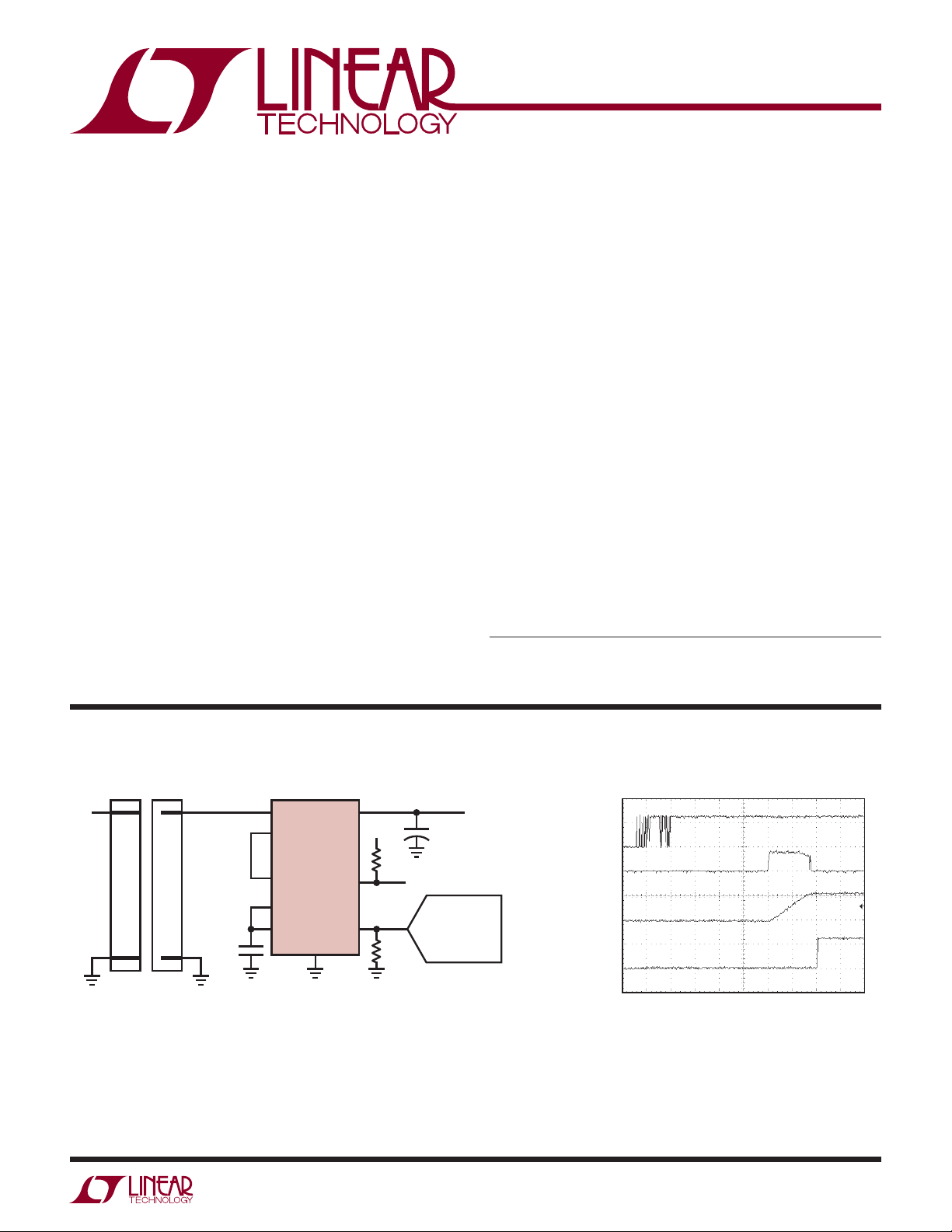
TYPICAL APPLICATION
12V, 1.5A Card Resident Application
12V
AUTO
RETRY
0.1μF
V
DD
UV
LTC4217DHC-12
FLT
TIMER
INTV
CC
GND
OUT
I
MON
PG
12V
10k
20k
Power-Up Waveforms
V
OUT
330μF
ADC
12V
1.5A
4217 TA01a
V
10V/DIV
0.1A/DIV
V
OUT
10V/DIV
10V/DIV
IN
I
IN
P
G
25ms/DIV
4217 TA01b
4217fb
+
1
LTC4217
(
ABSOLUTE MAXIMUM RATINGS
(Notes 1, 2)
Supply Voltage (VDD) ................................. –0.3V to 28V
Input Voltages
FB, OV, UV .............................................. –0.3V to 12V
TIMER ................................................... –0.3V to 3.5V
SENSE .............................V
– 10V or – 0.3V to V
DD
DD
Output Voltages
, I
I
SET
................................................. –0.3V to 3V
MON
PG, FLT .................................................. –0.3V to 35V
OUT ............................................–0.3V to V
INTV
.................................................. –0.3V to 3.5V
CC
+ 0.3V
DD
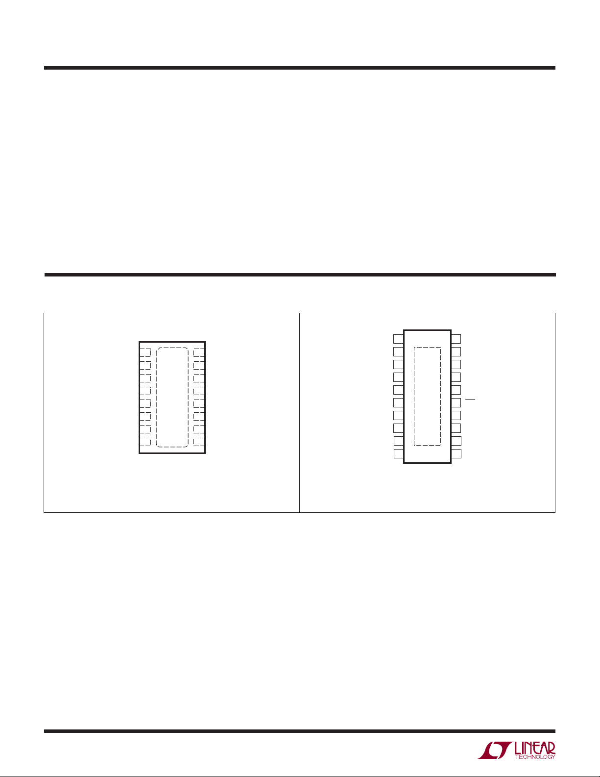
PACKAGE/ORDER INFORMATION
TOP VIEW
1
V
DD
2
UV
3
OV
4
TIMER
5
INTV
CC
6
GND
7
OUT
8
OUT
DHC PACKAGE
5mm s 3mm) PLASTIC DFN
16-LEAD
T
= 125°C, θJA = 43°C/W
JMAX
EXPOSED PAD (PIN 17) IS SENSE,
= 43°C/W SOLDERED, OTHERWISE θJA = 140°C/W
θ
JA
16
V
DD
15
I
SET
14
I
MON
13
17
FB
12
FLT
11
PG
10
GATE
9
OUT
GATE (Note 3) ........................................ –0.3V to 33V
Operating Temperature Range
LTC4217C ................................................ 0°C to 70°C
LTC4217I..............................................–40°C to 85°C
Junction Temperature (Notes 4, 5)........................ 125°C
Storage Temperature Range
DHC Package ..................................... –65°C to 125°C
FE Package ........................................–65°C to 150°C
Lead Temperature (Soldering, 10 sec)
FE Package Only ...............................................300°C
TOP VIEW
1
SENSE
2
V
DD
3
UV
4
OV
5
TIMER
INTV
CC
GND
OUT
OUT
SENSE
20-LEAD PLASTIC TSSOP
T
JMAX
EXPOSED PAD (PIN 21) IS SENSE,
= 38°C/W SOLDERED, OTHERWISE θJA = 130°C/W
θ
JA
21
6
7
8
9
10
FE PACKAGE
= 125°C, θJA = 38°C/W
SENSE
20
V
19
DD
I
18
SET
I
17
MON
FB
16
FLT
15
PG
14
GATE
13
OUT
12
SENSE
11
4217fb
2
LTC4217
ORDER INFORMATION
LEAD FREE FINISH TAPE AND REEL PART MARKING* PACKAGE DESCRIPTION TEMPERATURE RANGE
LTC4217CDHC-12#PBF LTC4217CDHC-12#TRPBF 421712
LTC4217IDHC-12#PBF LTC4217IDHC-12#TRPBF 421712
LTC4217CDHC#PBF LTC4217CDHC#TRPBF 4217
LTC4217IDHC#PBF LTC4217IDHC#TRPBF 4217
16-Lead (5mm × 3mm) Plastic DFN
16-Lead (5mm × 3mm) Plastic DFN
16-Lead (5mm × 3mm) Plastic DFN
16-Lead (5mm × 3mm) Plastic DFN
LTC4217CFE#PBF LTC4217CFE#TRPBF LTC4217FE 20-Lead Plastic TSSOP 0°C to 70°C
LTC4217IFE#PBF LTC4217IFE#TRPBF LTC4217FE 20-Lead Plastic TSSOP –40°C to 85°C
LEAD BASED FINISH TAPE AND REEL PART MARKING* PACKAGE DESCRIPTION TEMPERATURE RANGE
LTC4217CDHC-12 LTC4217CDHC-12#TR 421712
LTC4217IDHC-12 LTC4217IDHC-12#TR 421712
LTC4217CDHC LTC4217CDHC#TR 4217
LTC4217IDHC LTC4217IDHC#TR 4217
16-Lead (5mm × 3mm) Plastic DFN
16-Lead (5mm × 3mm) Plastic DFN
16-Lead (5mm × 3mm) Plastic DFN
16-Lead (5mm × 3mm) Plastic DFN
LTC4217CFE LTC4217CFE#TR LTC4217FE 20-Lead Plastic TSSOP 0°C to 70°C
LTC4217IFE LTC4217IFE#TR LTC4217FE 20-Lead Plastic TSSOP –40°C to 85°C
Consult LTC Marketing for parts specifi ed with wider operating temperature ranges. *The temperature grade is identifi ed by a label on the shipping container.
For more information on lead free part marking, go to:
For more information on tape and reel specifi cations, go to:
http://www.linear.com/leadfree/
http://www.linear.com/tapeandreel/
0°C to 70°C
–40°C to 85°C
0°C to 70°C
–40°C to 85°C
0°C to 70°C
–40°C to 85°C
0°C to 70°C
–40°C to 85°C
ELECTRICAL CHARACTERISTICS
The l denotes the specifi cations which apply over the full operating
temperature range, otherwise specifi cations are at TA = 25°C. VDD = 12V unless otherwise noted.
SYMBOL PARAMETER CONDITIONS MIN TYP MAX UNITS
DC Characteristics
V
DD
I
DD
V
DD(UVL)
V
DD(UVTH)
ΔV
DD(UVHYST)
V
DD(OVTH)
ΔV
DD(OVHYST)
V
OUT(PGTH)
ΔV
OUT(PGHYST)
I
OUT
ΔV
/Δt GATE Pin Turn-On Ramp Rate
GATE
R
ON
I
LIM(TH)
Input Supply Range
Input Supply Current MOSFET On, No Load
Input Supply Undervoltage Lockout VDD Rising
Input Supply Undervoltage Threshold LTC4217-12 Only, VDD Rising
Input Supply Undervoltage Hysteresis LTC4217-12 Only
Input Supply Overvoltage Threshold LTC4217-12 Only, VDD Rising
Input Supply Overvoltage Hysteresis LTC4217-12 Only
Output Powergood Threshold LTC4217-12 Only, V
Output Powergood Hysteresis LTC4217-12 Only
OUT Pin Leakage Current V
MOSFET + Sense Resistor On Resistance Note 6
Current Limit Threshold VFB = 1.23V 1.9 2 2.1 A
= V
OUT
V
= V
OUT
V
= V
OUT
= 1.23V
V
FB
VFB = 0V
= 1.23V, R
V
FB
Rising
OUT
= 0V, VDD = 26.5V
GATE
= 12V, LTC4217 Only
GATE
= 12V, LTC4217-12 Only
GATE
= 20kΩ
SET
l
2.9 26.5 V
l
l
2.65 2.73 2.85 V
l
9.6 9.88 10.2 V
l
520 640 760 mV
l
14.7 15.05 15.4 V
l
183 244 305 mV
l
10.2 10.5 10.8 V
l
127 170 213 mV
l
l
1
l
50
l
0.15 0.3 0.55 V/ms
l
15 32 50
l
1.85 2 2.15 A
l
0.35 0.5 0.7 A
l
0.85 1 1.17 A
1.6 3 mA
0
±150
2
70
90
4
mΩ
μA
μA
μA
4217fb
3
LTC4217
ELECTRICAL CHARACTERISTICS
The l denotes the specifi cations which apply over the full operating
temperature range, otherwise specifi cations are at T
SYMBOL PARAMETER CONDITIONS MIN TYP MAX UNITS
Inputs
I
IN
R
IN
V
TH
ΔV
OV(HYST)
ΔV
UV(HYST)
V
UV(RTH)
ΔV
FB(HYST)
R
ISET
Outputs
V
OL
I
OH
V
TIMER(H)
V
TIMER(L)
I
TIMER(UP)
I
TIMER(DN)
I
TIMER(RATIO)
A
IMON
I
OFF(IMON)
I
GATE(UP)
I
GATE(DN)
I
GATE(FST)
AC Characteristics
t
PHL(GATE)
t
PHL(ILIM)
t
D(ON)
t
D(CB)
t
D(AUTO-RETRY)
OV, UV, FB Pin Input Current VIN = 1.2V, LTC4217 Only
OV, UV, FB Pin Input Resistance LTC4217-12 Only
OV, UV, FB Pin Threshold Voltage VIN Rising
OV Pin Hysteresis
UV Pin Hysteresis
UV Pin Reset Threshold Voltage VUV Falling
FB Pin Power Good Hysteresis
I
Pin Output Resistor
SET
PG, FLT Pin Output Low Voltage I
PG, FLT Pin Input Leakage Current V
TIMER Pin High Threshold V
TIMER Pin Low Threshold V
TIMER Pin Pull-Up Current V
TIMER Pin Pull-Down Current V
TIMER Pin Current Ratio I
I
Pin Current Gain I
MON
I
Pin Offset Current I
MON
TIMER(DN)/ITIMER(UP)
Gate Pull-Up Current Gate Drive On, V
Gate Pull-Down Current Gate Drive Off, V
Gate Fast Pull-Down Current Fast Turn Off, V
Input High (OV), Input Low (UV) to Gate Low
Propagation Delay
Short Circuit to Gate Low VFB = 0, Step I
Turn-On Delay Step VUV to 2V, V
Circuit Breaker Filter Delay Time (Internal) VFB = 0V, Step I
Auto-Retry Turn-On Delay (Internal)
= 25°C. VDD = 12V unless otherwise noted.
A
= 2mA
OUT
= 30V
OUT
Rising
TIMER
Falling
TIMER
= 0V
TIMER
= 1.2V
TIMER
= 2A
OUT
= 132mA
OUT
V
< 16.5V Falling
GATE
V
< 16.5V Falling
GATE
GATE
GATE
GATE
SENSE
GATE
SENSE
= V
= 18V, V
= 18V, V
to 1.2A,
> 13V
to 1.2A
= 12V
SOURCE
= 12V
OUT
= 12V 140 mA
OUT
l
l
13 18 23
l
1.21 1.235 1.26 V
l
10 20 30 mV
l
50 80 110 mV
l
0.55 0.62 0.7 V
l
10 20 30 mV
l
19.5 20 20.5
l
l
l
1.2 1.235 1.28 V
l
0.1 0.21 0.3 V
l
–80 –100 –120 μA
l
1.4 2 2.6 μA
l
1.6 2 2.7 %
l
47.5 50 52.5 μA/A
l
l
–19 –24 –29 μA
l
190 250 340 μA
l
l
l
50 100 150 ms
l
1.5 2 2.7 ms
l
50 100 150 ms
0±1 μA
0.4 0.8 V
0 ±10 μA
0 ±7.5 μA
810 μs
15 μs
kΩ
kΩ
Note 1: Stresses beyond those listed under Absolute Maximum Ratings
may cause permanent damage to the device. Exposure to any Absolute
Maximum Rating condition for extended periods may affect device
reliability and lifetime.
Note 2: All currents into pins are positive, all voltages are referenced to
GND unless otherwise specifi ed.
Note 3: An internal clamp limits the GATE pin to a maximum of 6.5V
above OUT. Driving this pin to voltages beyond the clamp may damage the
device.
Note 4: This IC includes overtemperature protection that is intended
to protect the device during momentary overload conditions. Junction
temperature will exceed 125°C when overtemperature protection is active.
Continuous operation above the specifi ed maximum operating junction
temperature may impair device reliability.
4
Note 5: T
dissipation, P
LTC4217DHC, LTC4217DHC-12: T
LTC4217FE: T
is calculated from the ambient temperature, TA, and power
J
, according to the formula:
D
= TA + (PD • 43°C/W)
J
= TA + (PD • 38°C/W)
J
Note 6: Switch on-resistance is guaranteed by design and test correlation
on the DHC package.
4217fb
LTC4217
TYPICAL PERFORMANCE CHARACTERISTICS
2.0
1.8
1.6
(mA)
DD
I
1.4
1.2
1.0
IDD vs V
0
DD
85°C
25°C
–40°C
5 101520
VDD (V)
UV Hysteresis vs Temperature
0.10
25 30
4217 G01
INTVCC Load Regulation
3.5
3.0
2.5
2.0
(V)
CC
1.5
INTV
1.0
0.5
0
0
I
LOAD
Timer Pull-Up Current vs
Temperature
–110
VDD = 3.3V
(mA)
T
= 25°C, VDD = 12V unless otherwise noted.
A
UV Low-High Threshold vs
Temperature
1.234
VDD = 5V
1.232
1.230
1.228
UV LOW-HIGH HRESHOLD (V)
1.226
–50
–14–12–10–8–6–4–2
4217 G02
–25 0 25
TEMPERATURE (°C)
Current Limit Delay
vs Overdrive)
1000
(t
PHL(ILIM)
50 75 100
4217 G03
0.08
0.06
UV HYSTERESIS (V)
0.04
–25 0 25
–50
TEMPERATURE (°C)
Current Limit Threshold Foldback
2.5
2.0
1.5
1.0
CURRENT LIMIT VALUE (A)
0.5
0
0.2 0.4 0.6 0.8
0
FB VOLTAGE (V)
50 75 100
4217 G04
1.0 1.2
4217 G07
–105
–100
–95
TIMER PULL-UP CURRENT (μA)
–90
–50
–25 0 25
TEMPERATURE (°C)
Current Limit Adjustment
(I
CURRENT LIMIT THRESHOLD VALUE (A)
2.5
2.0
1.5
1.0
0.5
vs R
OUT
0
1k
)I
SET
10k 100k 1M
R
SET
50 75 100
(Ω)
4217 G05
4217 G08
10M
100
10
1
CURRENT LIMIT PROPAGATION DELAY (μs)
0.1
22
21
20
RESISTOR (kΩ)
SET
I
19
18
2468
010
SET
–50
OUTPUT CURRENT (A)
Resistor vs Temperature
–25 0 25
TEMPERATURE (°C)
50 75 100
4217 G06
4217 G09
4217fb
5

LTC4217
TYPICAL PERFORMANCE CHARACTERISTICS
RON vs VDD and Temperature MOSFET SOA Curve
60
50
40
30
(mΩ)
ON
R
20
10
0
–50
I
MON
105
VDD = 3.3V, 12V, 24V
I
LOAD
100
95
(μA)
MON
I
90
85
VDD = 3.3V, 12V, 24V
–25 0 25
TEMPERATURE (°C)
50 75 100
vs Temperature and V
= 2A
4217 G10
DD
10
1
(A)
D
I
0.1
TA = 25°C
MULTIPLE PULSE
DUTY CYCLE = 0.2
0.01
0.1
1 10 100
GATE Pull-Up Current vs
Temperature
–26.0
–25.5
–25.0
PULL-UP (μA)
GATE
I
–24.5
VDS (V)
TA = 25°C, VDD = 12V unless otherwise noted.
1ms
10ms
100ms
1s
10s
DC
4217 G11
LOW (V)
OUT
PG, FLT V
14
12
10
8
6
4
2
0
PG, FLT V
0
Low vs I
OUT
2468
I
LOAD
PG
(mA)
LOAD
FLT
Gate Pull-Up Current vs
Gate Drive
7
6
) (V)
5
SOURCE
4
– V
GATE
3
2
1
GATE DRIVE (V
VDD = 12V
VDD = 3.3V
10 12
4217 G12
80
6.2
) (V)
6.0
SOURCE
5.8
– V
GATE
5.6
5.4
GATE DRIVE (V
5.2
6
–50
–25 0 25
TEMPERATURE (°C)
Gate Drive vs V
0
51015
DD
VDD (V)
50 75 100
4217 G13
20 25 30
4217 G16
–24.0
–50
–25 0 25
TEMPERATURE (°C)
Gate Drive vs Temperature
6.15
) (V)
6.14
SOURCE
6.13
– V
GATE
6.12
6.11
GATE DRIVE (V
6.10
–50
–25 0 25
TEMPERATURE (°C)
50 75 100
4217 G14
50 75 100
4217 G17
(V)
ISET
V
0.9
0.8
0.7
0.6
0.5
0.4
0.3
0
–50
0
V
ISET
–25 0 25
–5 –10 –15 –20
I
GATE
(μA)
vs Temperature
50 75 150125100
TEMPERATURE (°C)
–25 –30
4217 G15
4217 G18
4217fb

PIN FUNCTIONS
LTC4217
Exposed Pad: SENSE.
FB: Foldback and Power Good Input. Connect this pin to
an external resistive divider from OUT for the LTC4217
(adjustable) version. The LTC4217-12 version uses a fi xed
internal divider with optional external adjustment. Open
the pin if the LTC4217-12 thresholds for 12V operation are
desired. If the voltage falls below 0.6V the current limit is
reduced using a foldback profi le (see Typical Performance
Characteristics). If the voltage falls below 1.21V the PG
pin will pull low to indicate the power is bad.
FLT: Overcurrent Fault Indicator. Open-drain output pulls
low when an overcurrent fault has occurred and the circuit
breaker trips. For overcurrent auto-retry tie to UV pin (see
Applications Information for details).
GATE: Gate Drive for Internal N-Channel MOSFET. An
internal 24μA current source charges the gate of the
N-channel MOSFET. At start-up the GATE pin ramps up at
a 0.3V/ms rate determined by internal circuitry. During an
undervoltage or overvoltage condition a 250μA pull-down
current turns the MOSFET off. During a short circuit or
undervoltage lockout condition, a 170mA pull-down current source between GATE and OUT is activated.
comparator monitors an internal resistive divider between
the OUT pin and GND.
OV: Overvoltage Comparator Input. Connect this pin to an
external resistive divider from V
for the LTC4217 (adjust-
DD
able) version. The LTC4217-12 version uses a fi xed internal
divider with optional external adjustment for 12V operation.
Open the pin if the LTC4217-12 thresholds are desired. If
the voltage at this pin rises above 1.235V, an overvoltage is
detected and the switch turns off. Tie to GND if unused.
PG: Power Good Indicator. Open-drain output pulls low
when the FB pin drops below 1.21V indicating the power is
bad. If the FB pin rises above 1.23V and the GATE to OUT
voltage exceeds 4.2V, the open-drain pull-down releases
the PG pin to go high.
SENSE: Current Sense Node and MOSFET Drain. The
current limit circuit controls the GATE pin to limit the
sense voltage between the V
and SENSE pins to 15mV
DD
(2A) or less depending on the voltage at the FB pin. The
Exposed Pad on DHC and FE packages are connected to
SENSE and must be soldered to an electrically isolated
printed circuit board trace to properly transfer the heat
out of the package.
GND: Device Ground.
I
: Current Monitor Output. The current in the internal
MON
MOSFET switch is divided by 20,000 and sourced from this
pin. Placing a 20k resistor from this pin to GND creates a 0V
to 2V voltage swing when current ranges from 0A to 2A.
INTV
: Internal 3V Supply Decoupling Output. This pin
CC
must have a 0.1μF or larger bypass capacitor.
I
: Current Limit Adjustment Pin. For 2A current limit value
SET
open this pin. This pin is driven by a 20k resistor in series
with a voltage source. The pin voltage is used to generate
the current limit threshold. The internal 20k resistor and
an external resistor between I
and ground create an
SET
attenuator that lowers the current limit value. In order to
match the temperature variation of the sense resistor, the
voltage on this pin increases at the same rate as the sense
resistance increases. Therefore the voltage at I
SET
pin is
proportional to temperature of the MOSFET switch.
OUT: Output of Internal MOSFET Switch. Connect this pin
directly to the load. In the LTC4217-12 version, the PG
TIMER: Timer Input. Connect a capacitor between this pin
and ground to set a 12ms/μF duration for current limit
before the switch is turned off. If the UV pin is toggled
low while the MOSFET switch is off, the switch will turn on
again following an cool down time of 518ms/μF duration.
Tie this pin to INTV
for a fi xed 2ms overcurrent delay
CC
and 100ms auto-retry time.
UV: Undervoltage Comparator Input. Tie high if unused.
Connect this pin to an external resistive divider from V
DD
for
the LTC4217 (adjustable) version. The LTC4217-12 version
drives the UV pin with an internal resistive divider from
V
. Open the pin if the preset LTC4217-12 thresholds for
DD
12V operation are desired. If the UV pin voltage falls below
1.15V, an undervoltage is detected and the switch turns
off. Pulling this pin below 0.62V resets the overcurrent
fault and allows the switch to turn back on (see Applications Information for details). If overcurrent auto-retry is
desired then tie this pin to the FLT pin.
V
: Supply Voltage and Current Sense Input. This pin
DD
has an undervoltage lockout threshold of 2.73V.
4217fb
7

LTC4217
FUNCTIONAL DIAGRAM
SENSE
(EXPOSED PAD)
INTERNAL 7.5mΩ
V
DD
SENSE RESISTOR
–
UV
OV
140k
20k
224k
20k
+–
V
DD
1.235V
*
+
–
*
0.62V
V
DD
*
+
–
+
*
1.235V
–
+
CM
UV
RST
OV
INTERNAL 20mΩ
0.2V
MOSFET
CHARGE
PUMP
AND GATE
DRIVER
+
TM1
–
INRUSHCS
OUT
LOGIC
GATE
0.3V/ms
100μA
2μA
INTV
CC
CLAMP
0.6V POSITIVE
TEMPERATURE
COEFFICIENT
REFERENCE
FOLDBACK
PG
OUT
I
MON
I
SET
20k
X1
FB
0.6V
+
–
1.235V
150k
20k
OUT
*
*
PG
FLT
+
V
V
2.73V
TM2
–
DD
UVLO1
1.235V
–
+
3.1V
GEN
DD
INTV
CC
–
TIMER
8
*LTC4217-12 (DFN) ONLY
GND
UVLO2
+
2.65V
4217 BD
4217fb

OPERATION
LTC4217
The Functional Diagram displays the main circuits of the
device. The LTC4217 is designed to turn a board’s supply
voltage on and off in a controlled manner allowing the board
to be safely inserted and removed from a live backplane.
The LTC4217 includes a 20mΩ MOSFET and a 7.5mΩ current sense resistor. During normal operation, the charge
pump and gate driver turn on the pass MOSFET’s gate to
provide power to the load. The inrush current control is
accomplished by the INRUSH circuit. This circuit limits
the GATE ramp rate to 0.3V/ms and hence controls the
voltage ramp rate of the output capacitor.
The current sense (CS) amplifi er monitors the load current
using the voltage sensed across the current sense resistor.
The CS amplifi er limits the current in the load by reducing the GATE-to-OUT voltage in an active control loop. It
is simple to adjust the current limit threshold using the
current setting (I
during other times such as start-up.
A short circuit on the output to ground causes signifi cant
power dissipation during active current limiting. To limit
this power, the foldback amplifi er reduces the current limit
value from 2A to 0.5A in a linear manner as the FB pin drops
below 0.6V (see Typical Performance Characteristics).
If an overcurrent condition persists, the TIMER pin ramps
up with a 100μA current source until the pin voltage exceeds 1.2V (comparator TM2). This indicates to the logic
that it is time to turn off the pass MOSFET to prevent
overheating. At this point the TIMER pin ramps down using the 2μA current source until the voltage drops below
0.2V (Comparator TM1) which tells the logic to start an
internal 100ms timer. At this point, the pass transistor
has cooled and it is safe to turn it on again. It is suitable
) pin. This allows a different threshold
SET
for many applications to use an internal 2ms overcurrent
timer with a 100ms cool down period. Tying the TIMER
pin to INTV
The fi xed 12V version, LTC4217-12, uses two separate
internal dividers from V
This version also features a divider from OUT to drive the
FB pin. The LTC4217-12 is available in the DFN package
while the LTC4217 (adjustable version) is in the DFN and
TSSOP packages.
The output voltage is monitored using the FB pin and the
PG comparator to determine if the power is available for
the load. The power good condition is signaled by the PG
pin using an open-drain pull-down transistor.
The Functional Diagram also shows the monitoring blocks
of the LTC4217. The two comparators on the left side
include the UV and OV comparators. These comparators
determine if the external conditions are valid prior to turning
on the MOSFET. But fi rst the undervoltage lockout circuits
UVLO1 and UVLO2 must validate the input supply and
the internally generated 3.1V supply (INTV
ate the power up initialization to the logic circuits. If the
external conditions remain valid for 100ms the MOSFET
is allowed to turn on.
Other features include MOSFET current and temperature
monitoring. The current monitor (CM) outputs a current
proportional to the sense resistor current. This current can
drive an external resistor or other circuits for monitoring
purposes. A voltage proportional to the MOSFET temperature is output to the I
allows external circuits to predict failure and shutdown
the system.
sets this default timing.
CC
to drive the UV and OV pins.
DD
pin. The MOSFET temperature
SET
) and gener-
CC
APPLICATIONS INFORMATION
The typical LTC4217 application is in a high availability
system that uses a positive voltage supply to distribute
power to individual cards. A complete application circuit
is shown in Figure 1. External component selection is
discussed in detail in the following sections.
Turn-On Sequence
Several conditions must be present before the internal pass
MOSFET can be turned on. First the supply V
its undervoltage lockout level. Next the internally generated
supply INTV
This generates a 25μs power-on-reset pulse which clears
the fault register and initializes internal latches.
must cross its 2.65V undervoltage threshold.
CC
must exceed
DD
4217fb
9

LTC4217
APPLICATIONS INFORMATION
12V
V
DD
R3
140k
UV
FLT
OV
R4
20k
TIMER
INTV
C1
0.1μF
R1
224k
R2
20k
C
T
0.1μF
Figure 1. 0.8A, 12V Card Resident Application
LTC4217FE
CC
GND
OUT
GATE
I
I
MON
R5
R
1k
R
20k
R
20k
GATE
C
0.1μF
SET
MON
GATE
150k
20k
R6
12V
FB
PG
SET
R7
10k
V
OUT
12V
0.8V
+
C
L
330μF
is a graph of the Safe Operating Area for the MOSFET. It is
evident from this graph that the power dissipation at 12V,
300mA for 40ms is in the safe region.
Adding a capacitor and a 1k series resistor from GATE
to ground will lower the inrush current below the default
value set by the INRUSH circuit. The GATE is charged
with an 24μA current source (when INRUSH circuit is
not driving the GATE). The voltage at the GATE pin rises
ADC
4217 F01
with a slope equal to 24μA/C
current is set at:
C
L
= •24
C
GATE
µA
I
INRUSH
and the supply inrush
GATE
After the power-on-reset pulse, the LTC4217 will go through
the following sequence. First, the UV and OV pins must
indicate that the input voltage is within the acceptable range.
All of these conditions must be satisfi ed for the duration
of 100ms to ensure that any contact bounce during the
insertion has ended.
The MOSFET is turned on by charging up the GATE with a
charge pump generated current source whose value is adjusted by shunting a portion of the pull-up current to ground.
The charging current is controlled by the INRUSH circuit
that maintains a constant slope of GATE voltage versus time
(Figure 2). The voltage at the GATE pin rises with a slope of
0.3V/ms and the supply inrush current is set at:
I
= CL • (0.3V/ms)
INRUSH
This gate slope is designed to charge up a 1000μF capacitor to 12V in 40ms, with an inrush current of 300mA.
This allows the inrush current to stay under the current
limit threshold (500mA) for capacitors less than 1000μF.
Included in the Typical Performance Characteristics section
V
+ 6.15
DD
SLOPE = 0.3V/ms
V
DD
GATE
OUT
When the GATE voltage reaches the MOSFET threshold
voltage, the switch begins to turn on and the OUT voltage follows the GATE voltage as it increases. Once OUT
reaches V
, the GATE will ramp up until clamped by the
DD
6.15V zener between GATE and OUT.
As the OUT voltage rises, so will the FB pin which is monitoring it. Once the FB pin crosses its 1.235V threshold and
the GATE to OUT voltage exceeds 4.2V, the PG pin will cease
to pull low and indicate that the power is good.
Parasitic MOSFET Oscillation
When the N-channel MOSFET ramps up the output during power-up it operates as a source follower. The source
follower confi guration may self-oscillate in the range of
25kHz to 300kHz when the load capacitance is less than
10μF, especially if the wiring inductance from the supply
to the V
pin is greater than 3μH. The possibility of oscil-
DD
lation will increase as the load current (during power-up)
increases. There are two ways to prevent this type of
oscillation. The simplest way is to avoid load capacitances
below 10μF. For wiring inductance larger than 20μH, the
minimum load capacitance may extend to 100μF. A second
choice is to connect an external gate capacitor C
>1.5nF
P
as shown in Figure 3.
10
t1 t2
Figure 2. Supply Turn-On
4217 F02
Turn-Off Sequence
The switch can be turned off by a variety of conditions. A
normal turn-off is initiated by the UV pin going below its
1.235V threshold. Additionally, several fault conditions
4217fb

APPLICATIONS INFORMATION
LTC4217
LTC4217
GATE
C
2.2nF
4217 F03
Figure 3. Compensation for Small C
P
*OPTIONAL
RC TO LOWER
INRUSH CURRENT
LOAD
will turn off the switch. These include an input overvoltage
(OV pin), overcurrent circuit breaker (SENSE pin) or over
temperature. Normally the switch is turned off with a 250μA
current pulling down the GATE pin to ground. With the
switch turned off, the OUT voltage drops which pulls the
FB pin below its threshold. PG then pulls low to indicate
output power is no longer good.
drops below 2.65V for greater than 5μs or INTVCC
If V
DD
drops below 2.5V for greater than 1μs, a fast shutdown
of the switch is initiated. The GATE is pulled down with a
170mA current to the OUT pin.
Overcurrent Fault
The LTC4217 features an adjustable current limit with
foldback that protects against short circuits or excessive
load current. To prevent excessive power dissipation in the
switch during active current limit, the available current is
reduced as a function of the output voltage sensed by the
FB pin. A graph in the Typical Performance curves shows
the current limit versus FB voltage.
An overcurrent fault occurs when the current limit circuitry
has been engaged for longer than the time-out delay set
by the TIMER. Current limiting begins when the MOSFET
current reaches 0.5A to 2A (depending on the foldback).
The GATE pin is then brought down with a 170mA GATEto-OUT current. The voltage on the GATE is regulated in
order to limit the current to less than 2A. At this point, a
circuit breaker time delay starts by charging the external
timing capacitor from the TIMER pin with a 100μA pull-up
current. If the TIMER pin reaches its 1.2V threshold, the
internal switch turns off (with a 250μA current from GATE
to ground). Included in the Typical Performance Curves is
a graph of the Safe Operating Area for the MOSFET. From
this graph one can determine the MOSFET’s maximum
time in current limit for a given output power.
Tying the TIMER pin to INTVCC will force the part to use
the internally generated (circuit breaker) delay of 2ms.
In either case the FLT pin is pulled low to indicate an
overcurrent fault has turned off the pass MOSFET. For a
given the circuit breaker time delay, the equation for setting
the timing capacitor’s value is as follows:
= tCB • 0.083(μF/ms)
C
T
After the switch is turned off, the TIMER pin begins discharging the timing capacitor with a 2μA pull-down current.
When the TIMER pin reaches its 0.2V threshold, an internal
100ms timer is started. After the 100ms delay, the switch
is allowed to turn on again if the overcurrent fault has been
cleared. Bringing the UV pin below 0.6V and then high will
clear the fault. If the TIMER pin is tied to INTV
then the
CC
switch is allowed to turn on again (after an internal 100ms
delay) if the overcurrent fault is cleared.
Tying the FLT pin to the UV pin allows the part to self-
clear the fault and turn the MOSFET on as soon as TIMER
pin has ramped below 0.2V. In this auto-retry mode the
LTC4217 repeatedly tries to turn on after an overcurrent
at a period determined by the capacitor on the TIMER pin.
The auto-retry mode also functions when the TIMER pin
is tied to INTV
CC
.
The waveform in Figure 4 shows how the output latches
off following a short circuit. The current in the MOSFET
is 0.5A as the timer ramps up.
Current Limit Adjustment
The default value of the active current limit is 2A. The
current limit threshold can be adjusted lower by placing
V
OUT
10V/DIV
I
OUT
1A/DIV
ΔV
GATE
10V/DIV
TIMER
2V/DIV
1ms/DIV
Figure 4. Short-Circuit Waveform
4217 F04
4217fb
11

LTC4217
APPLICATIONS INFORMATION
a resistor between the I
the Functional Diagram the voltage at the I
pin and ground. As shown in
SET
pin (via
SET
the clamp circuit) sets the CS amplifi er’s built-in offset
voltage. This offset voltage directly determines the active
current limit value. With the I
the I
pin is determined by a positive temperature co-
SET
pin open, the voltage at
SET
effi cient reference. This voltage is set to 0.618V at room
temperature which corresponds to a 2A current limit at
room temperature.
An external resistor placed between the I
pin and ground
SET
forms a resistive divider with the internal 20k sourcing
resistor. The divider acts to lower the voltage at the I
SET
pin and therefore lower the current limit threshold. The
overall current limit threshold precision is reduced to ±11%
when using a 20k resistor to half the threshold.
Using a switch (connected to ground) in series with this
external resistor allows the active current limit to change
only when the switch is closed. This feature can be used
when the startup current exceeds the typical maximum
load current.
tor that is charged with this current. When the capacitor
voltage trips the comparator and the capacitor is reset, a
timer is started. The time between resets will indicate the
MOSFET current.
Monitor OV and UV Faults
Protecting the load from an overvoltage condition is the
main function of the OV pin. In the LTC4217-12 an internal
resistive divider (driving the OV pin) connects to a comparator to turn off the MOSFET when the V
15.05V. If the V
pin subsequently falls back below 14.8V,
DD
voltage exceeds
DD
the switch will be allowed to turn on immediately. In the
LTC4217 the OV pin threshold is 1.23V when rising and
1.21V when falling out of overvoltage.
The UV pin functions as an undervoltage protection pin or
as an “ON” pin. In the LTC4217-12 the MOSFET turns off
when V
falls below 9.23V. If the VDD pin subsequently
DD
rises above 9.88V for 100ms, the switch will be allowed
to turn on again. The LTC4217 UV turn on/off threshold
is 1.23V (rising) and 1.15V (falling).
Monitor MOSFET Temperature
The voltage at the I
ing temperature. The temperature profi le of the I
pin increases linearly with increas-
SET
SET
pin
is shown in Typical Performance Characteristics. Using a
comparator or ADC to measure the I
voltage provides
SET
an indicator of the MOSFET temperature.
There is an over-temp circuit in the LTC4217 that monitors
an internal voltage similar to the I
pin voltage. When
SET
the die temperature exceeds 145°C the circuit turns off
the MOSFET until the temperature drops to 125°C.
Monitor MOSFET Current
The current in the MOSFET passes through a sense resistor.
The voltage on the sense resistor is converted to a current
that is sourced out of the I
amplifi er is 50μA from I
MON
pin. The gain of I
MON
for 1A of MOSFET current.
SENSE
This output current can be converted to a voltage using an
external resistor to drive a comparator or ADC. The voltage
compliance for the I
pin is from 0V to INTVCC – 0.7V.
MON
A microcontroller with a built-in comparator can build a
simple integrating single-slope ADC by resetting a capaci-
In the cases of an undervoltage or over voltage the MOSFET
turns off and there is indication on the PG status pin. When
the overvoltage is removed the MOSFET’s gate ramps
up immediately at the rate determined by the INRUSH
block.
Power Good Indication
In addition to setting the foldback current limit threshold,
the FB pin is used to determine a power good condition.
The LTC4217-12 uses an internal resistive divider on the
OUT pin to drive the FB pin. The PG comparator indicates
logic high when OUT pin rises above 10.5V. If the OUT pin
subsequently falls below 10.3V the comparator toggles low.
On the LTC4217 the PG comparator drives high when the FB
pin rises above 1.23V and low when falls below 1.21V.
Once the PG comparator is high the GATE pin voltage is
monitored with respect to the OUT pin. Once the GATE
minus OUT voltage exceeds 4.2V the PG pin goes high.
This indicates to the system that it is safe to load the OUT
pin while the MOSFET is completely turned “on”. The PG
pin goes low when the GATE is commanded off (using
the UV, OV or SENSE pins) or when the PG comparator
drives low.
4217fb
12

APPLICATIONS INFORMATION
LTC4217
12V Fixed Version
In the LTC4217-12 the UV, OV and FB pins are driven by
internal dividers which may need to be fi ltered to prevent
false faults. By placing a bypass capacitor on these pins
the faults are delayed by the RC time constant. Use the R
IN
value from the electrical table for this calculation.
In cases where the fi xed thresholds need a slight adjustment, placing a resistor from the UV or OV pins to V
DD
or GND will adjust the threshold up or down. Likewise
placing a resistor between FB pin to OUT or GND adjusts
the threshold. Again use the R
value from the electrical
IN
table for this calculation.
An example in Figure 5 raises the UV turn-on voltage from
9.88V to 10.5V. Increasing the UV level requires adding a
resistor between UV and ground. The resistor, R
SHUNT1
,
can be calculated using electrical table parameters as
follows:
RV
•
OLD
IN
()
R
SHUNT
=
1
VV
()
–
NEW OLD
18 9 88
k
=
•.
10 5
()
.–
9988
.
287
= k
In this same fi gure the OV threshold is lowered from
15.05V to 13.5V. Decreasing the OV threshold requires
adding a resistor between V
and OV. This resistor can
DD
be calculated as follows:
⎞
()
⎟
=
⎟
⎟
⎠
R
SHUNT
k
18 15 05
1 235
RV
•
IN
()
=
2
•.
.
Figure 5. Adjusting LTC4217-12 Thresholds
V
TH
()
⎛
13 5 1 235
()
⎜
115 05 13 5
()
⎝
⎛
()
OLD
⎜
⎜
⎜
⎝
.–.
.–.
LTC4217-12
4217 F05
–
VV
NEW
VV
()
OLD
–
OV TH
NNEW
⎞
1 736
.
= M
⎟
⎠
V
DD
R
SHUNT2
OV
UV
R
SHUNT1
Use the equation for R
SHUNT1
FB thresholds. Likewise use the equation for R
for increasing the OV and
SHUNT2
for
decreasing the UV and FB thresholds.
Design Example
Consider the following design example (Figure 6): V
12V, I
MAX
9.88V, V
= 2A. I
OVOFF
= 15.05V, V
= 100mA, CL = 330μF, V
INRUSH
= 10.5V. A current limit fault
PWRGD
IN
UVON
=
=
triggers an automatic restart of the power up sequence.
V
12V
V
DD
UV
LTC4217-12DHC
FLT
TIMER
INTV
C1
0.1μF
Figure 6. 1.5A, 12V Card Resident Application
OUT
PG
I
MON
CC
GND
12V
R1
10k
R2
20k
+
C
L
330μF
ADC
12V
1.5A
OUT
4217 F06
The inrush current is defi ned by the current required to
charge the output capacitor using the fi xed 0.3V/ms GATE
charge up rate. The inrush current is defi ned as:
IC
INRUSH L
=
V
.
⎛
⎜
⎝
ms
⎞
⎟
⎠
=
330
µF
V
.03
03
⎛
•
⎜
⎝
ms
⎞
=•
⎟
⎠
1100mA
As mentioned previously the charge up time is the output voltage (12V) divided by the output rate of 0.3V/ms
resulting in 40ms. The peak power dissipation of 12V at
100mA (or 1.2W) is within the SOA of the pass MOSFET
for 40ms (see MOSFET SOA curve in the Typical Performance Characteristics).
Next the power dissipated in the MOSFET during overcurrent
must be limited. The active current limit uses a timer to
prevent excessive energy dissipation in the MOSFET. The
worst-case power dissipation occurs when the voltage
versus current profi le of the foldback current limit is at
the maximum. This occurs when the current is 2A and the
voltage is one half of the 12V or 6V. See the Current Limit
Sense Voltage vs FB Voltage in the Typical Performance
Characteristics section to view this profi le. In order to
survive 12W, the MOSFET SOA dictates a maximum time
of 10ms (see SOA graph). Use the internal 2ms timer
4217fb
13

LTC4217
APPLICATIONS INFORMATION
invoked by tying the TIMER pin to INTVCC. After the 2ms
timeout the FLT pin needs to pull-down on the UV pin to
restart the power-up sequence.
Since the default values for overvoltage, undervoltage and
power good thresholds for the 12V fi xed version match
the requirements, no external components are required
for the UV, OV and FB pins.
The fi nal schematic in Figure 1 results in very few external
components. The pull-up resistor, R1, connects to the
PG pin while the 20k (R2) converts the I
current to a
MON
voltage at a ratio:
µA
V
IMON
50
==
201•
A
V
k
A
In addition there is a 0.1μF bypass (C1) on the INTVCC pin.
Layout Considerations
In Hot Swap applications where load currents can be 2A,
narrow PCB tracks exhibit more resistance than wider tracks
and operate at elevated temperatures. The minimum trace
width for 1oz copper foil is 0.02" per amp to make sure
the trace stays at a reasonable temperature. Using 0.03"
per amp or wider is recommended. Note that 1oz copper
exhibits a sheet resistance of about 0.5mΩ/square. Small
resistances add up quickly in high current applications.
There are two V
pins on opposite sides of the package
DD
that connect to the sense resistor and MOSFET. The PCB
layout should be balanced and symmetrical to each V
DD
pin to balance current in the MOSFET bond wires. Figure 7
shows a recommended layout for the LTC4217.
Although the MOSFET is self protected from overtemperature, it is recommended to solder the backside of the
package to a copper trace to provide a good heat sink. Note
that the backside is connected to the SENSE pin and cannot
be soldered to the ground plane. During normal loads the
power dissipated in the MOSFET is as high as 0.14W. A
10mm × 10mm area of 1oz copper should be suffi cient.
This area of copper can be divided in many layers.
It is also important to put C1, the bypass capacitor for
the INTV
pin as close as possible between the INTVCC
CC
and GND.
Additional Applications
The LTC4217 has a wide operating range from 2.9V to 26.5V.
The UV, OV and PG thresholds are set with few resistors.
All other functions are independent of supply voltage.
Figure 8 shows a 3.3V application with a UV threshold of
2.87V, an OV threshold of 3.77V and a PG threshold of
3.05V. The last page includes a 24V application with a UV
threshold of 19.9V, an OV threshold of 26.3V and a PG
threshold of 20.75V.
14
HEAT SINK
DD
VIA TO
SINK
C
Figure 7. Recommended Layout
OUTV
GND
4217 F07
3.3V
R1
17.4k
R2
3.16k
R3
10k
0.1μF
V
DD
UV
FLT
OV
TIMER
INTV
C
T
LTC4217FE
CC
GND
I
OUT
PG
MON
R4
14.7k
FB
3.3V
R6
10k
R
20k
R5
10k
MON
Figure 8. 3.3V, 1.5A Card Resident Application
V
OUT
3.3V
+
1.5A
C
L
100μF
ADC
4217 F08
4217fb

PACKAGE DESCRIPTION
LTC4217
DHC Package
16-Lead Plastic DFN (5mm × 3mm)
(Reference LTC DWG # 05-08-1706)
3.50 ±0.05
2.20 ±0.05
0.65 ±0.05
1.65 ±0.05
(2 SIDES)
0.25 ± 0.05
0.50 BSC
4.40 ±0.05
(2 SIDES)
RECOMMENDED SOLDER PAD PITCH AND DIMENSIONS
NOTE:
1. DRAWING PROPOSED TO BE MADE VARIATION OF VERSION (WJED-1) IN JEDEC
PACKAGE OUTLINE MO-229
2. DRAWING NOT TO SCALE
3. ALL DIMENSIONS ARE IN MILLIMETERS
PACKAGE
OUTLINE
TOP MARK
(SEE NOTE 6)
20-Lead Plastic TSSOP (4.4mm)
(Reference LTC DWG # 05-08-1663)
Exposed Pad Variation CA
4.95
(.195)
5.00 ±0.10
(2 SIDES)
PIN 1
0.200 REF
4. DIMENSIONS OF EXPOSED PAD ON BOTTOM OF PACKAGE DO NOT INCLUDE
MOLD FLASH. MOLD FLASH, IF PRESENT, SHALL NOT EXCEED 0.15mm ON ANY SIDE
5. EXPOSED PAD SHALL BE SOLDER PLATED
6. SHADED AREA IS ONLY A REFERENCE FOR PIN 1 LOCATION ON THE
TOP AND BOTTOM OF PACKAGE
3.00 ±0.10
(2 SIDES)
0.75 ±0.05
R = 0.20
1.65 ± 0.10
(2 SIDES)
0.00 – 0.05
TYP
FE Package
6.40 – 6.60*
(.252 – .260)
4.95
20 19 18 17 16 15
(.195)
111214 13
R = 0.115
TYP
0.25 ± 0.05
0.50 BSC
4.40 ±0.10
(2 SIDES)
BOTTOM VIEW—EXPOSED PAD
169
18
0.40 ± 0.10
PIN 1
NOTCH
(DHC16) DFN 1103
6.60 ±0.10
4.50 ±0.10
RECOMMENDED SOLDER PAD LAYOUT
0.09 – 0.20
(.0035 – .0079)
NOTE:
1. CONTROLLING DIMENSION: MILLIMETERS
2. DIMENSIONS ARE IN
3. DRAWING NOT TO SCALE
SEE NOTE 4
4.30 – 4.50*
(.169 – .177)
0.50 – 0.75
(.020 – .030)
MILLIMETERS
0.65 BSC
(INCHES)
2.74
(.108)
0.45 ±0.05
1.05 ±0.10
1345678910
2
0.25
REF
0° – 8°
0.65
(.0256)
BSC
0.195 – 0.30
(.0077 – .0118)
4. RECOMMENDED MINIMUM PCB METAL SIZE
FOR EXPOSED PAD ATTACHMENT
*DIMENSIONS DO NOT INCLUDE MOLD FLASH. MOLD FLASH
SHALL NOT EXCEED 0.150mm (.006") PER SIDE
TYP
Information furnished by Linear Technology Corporation is believed to be accurate and reliable.
However, no responsibility is assumed for its use. Linear Technology Corporation makes no representation that the interconnection of its circuits as described herein will not infringe on existing patent rights.
2.74
(.108)
1.20
(.047)
MAX
0.05 – 0.15
(.002 – .006)
FE20 (CA) TSSOP 0204
6.40
(.252)
BSC
4217fb
15

LTC4217
TYPICAL APPLICATION
24V, 1.5A Card Resident Application
24V V
*
200k
3.24k
10k
0.1μF
*DIODES INC. SMAJ24A
V
DD
UV
FLT
OV
TIMER
INTV
LTC4217FE
CC
GND
I
OUT
MON
PG
100μF
ADC
24V
1.5A
4217 TA02
OUT
158k
FB
24V
10k
20k
+
10k
RELATED PARTS
PART NUMBER DESCRIPTION COMMENTS
LTC1421 Dual Channel, Hot Swap Controller Operates from 3V to 12V, Supports –12V, SSOP-24
LTC1422 Single Channel, Hot Swap Controller Operates from 2.7V to 12V, SO-8
LTC1642A Single Channel, Hot Swap Controller Operates from 3V to 16.5V, Overvoltage Protection up to 33V, SSOP-16
LTC1645 Dual Channel, Hot Swap Controller Operates from 3V to 12V, Power Sequencing, SO-8 or SO-14
LTC1647-1/LTC1647-2/
LTC1647-3
LTC4210 Single Channel, Hot Swap Controller Operates from 2.7V to 16.5V, Active Current Limiting, SOT23-6
LTC4211 Single Channel, Hot Swap Controller Operates from 2.5V to 16.5V, Multifunction Current Control, MSOP-8 or MSOP-10
LTC4212 Single Channel, Hot Swap Controller Operates from 2.5V to 16.5V, Power-Up Timeout, MSOP-10
LTC4214 Negative Voltage, Hot Swap Controller Operates from –6V to –16V, MSOP-10
LTC4215 Hot Swap Controller with I
LTC4218 Single Channel, Hot Swap Controller Operates from 2.9V to 26.5V, Adjustable Current Limit, SSOP-16
LT4220 Positive and Negative Voltage, Dual
LTC4221 Dual Hot Swap Controller/Sequencer Operates from 1V to 13.5V, Multifunction Current Control, SSOP-16
LTC4230 Triple Channels, Hot Swap Controller Operates from 1.7V to 16.5V, Multifunction Current Control, SSOP-20
Dual Channel, Hot Swap Controller Operates from 2.7V to 16.5V, SO-8 or SSOP-16
2
C Compatible
Operates from 2.9V to 15V, 8-Bit ADC Monitors Current and Voltage
Monitoring
Operates from ±2.7V to ±16.5V, SSOP-16
Channels, Hot Swap Controller
16
Linear Technology Corporation
1630 McCarthy Blvd., Milpitas, CA 95035-7417
(408) 432-1900 ● FAX: (408) 434-0507
●
www.linear.com
4217fb
LT 1108 REV B • PRINTED IN USA
© LINEAR TECHNOLOGY CORPORATION 2008
 Loading...