

Page 1
advertisement
y
Electronic Circuit Breaker in Small DFN Package Eliminates Sense
Resistor – Design Note 402
SH Lim
Introduction
Traditionally, an Electronic Circuit Breaker (ECB) comprises a MOSFE T, a MOSFET controller and a curren t sense
®
resistor. The LTC
by using the R
4213 does away with the sense resistor
of the external MOSFET. The result
DS(ON)
is a simple, small solution that offers a signifi cant low
insertion loss advantage at low operating load voltage.
The LTC4213 features two circuit breaking responses to
varying overload conditions with three selectable trip
thresholds and a high side drive for an external N-channel MOSFET switch.
Overcurrent Protection
The SENSEP and SENSEN pins monitor the load current via the R
of the external MOSFET and serve
DS(ON)
as inputs to two internal comparators—SLOWCOMP
and FASTCOMP—with trip points at V
CB
and V
CB(FAST)
,
respectively. The circuit breaker trips when an overcurrent fault causes a substantial voltage drop across the
MOSFET. An overload current exceeding V
CB/RDS(ON)
causes SLOWCOMP to trip the cir cuit breaker after a 16µs
delay. In the event of a severe overload or short-circuit
current exceeding V
CB(FAST)/RDS(ON)
, the FASTCOMP
trips the circuit breaker within 1µs, protecting both the
MOSFET and the load.
Both of the comparators have a common mode input
voltage range from ground to V
+ 0.2V. This allows
CC
the circuit breaker to operate as the load supply turns
on from 0V.
Flexible Overcurrent Setting
The LTC4213 has an I
pin to select one of these three
SEL
overcurrent settings:
at GND, VCB = 25mV and V
I
SEL
I
left open, VCB = 50mV and V
SEL
I
at V
, V
SEL
CC
CB
= 100mV and V
CB(FAST)
CB(FAST)
CB(FAST)
= 100mV
= 175mV
= 325mV
Overvoltage Protection
The LTC4213 can provide load overvoltage protection
(OVP) above the bias supply. When V
SENSEP
> V
CC
for 65µs, an internal OVP circuit activates with the GATE
pin pulling low and the external MOSFET turning off. The
OVP circuit protects the system from an incorrect plug-in
event where the V
bias voltage.
V
CC
load supply is much higher than the
IN
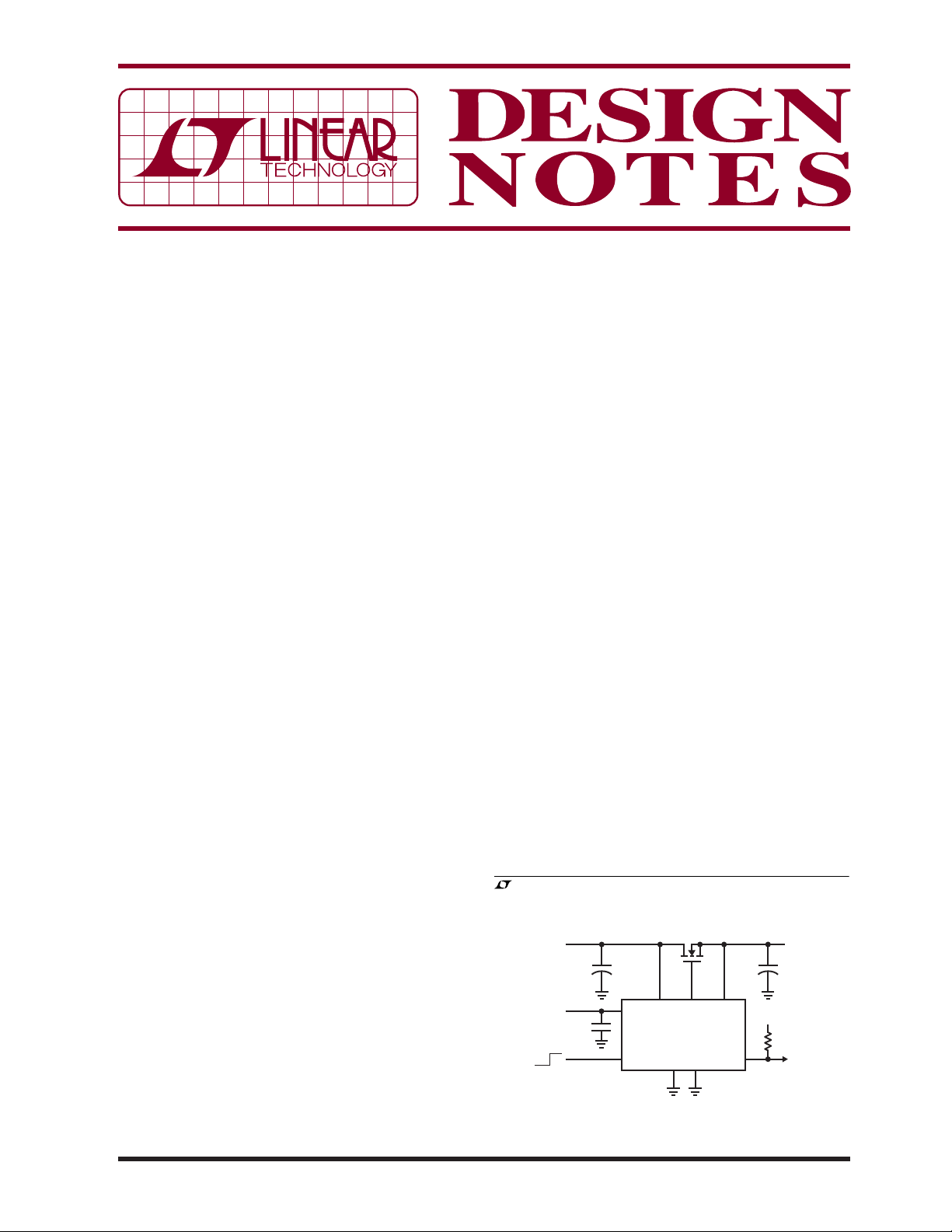
Typical Electronic Circuit Breaker (ECB)
Application
Figure 1 shows the LTC4213 in a dual supply ECB application. An input bypass capacitor is recommended to
prevent transient spikes when the V
supply powers-up
IN
or the ECB responds to overcurrent conditions. Figure 2
shows a normal power-up sequence. The LTC4213 exits
reset mode once the V
pin is above the internal under
CC
voltage lockout threshold and the ON pin rises above
0.8V (see trace 1 in Figure 2). After an internal 60µs debounce cycle, the GATE pin capacitance is charged up
from ground by an internal 100µA current source (see
trace 2). As the GATE pin and the gate of MOSFET charges
up, the external MOSFET turns on when V
GATE
exceeds
the MOSFET’s threshold. The circuit breaker is armed
when V
exceeds ΔV
GATE
, a voltage at which the
GSARM
external MOSFET is deemed fully enhanced and R
, LT, LTC, LTM and Burst Mode are registered trademarks of Linear Technolog
Corporation. All other trademarks are the property of their respective owners.
Q1
1.25V
V
BIAS
3.3V
OFF ON
V
IN
+
C
IN
100µF
V
C1
0.1µF
ON READY
SI4864DY
C
LOAD
100µF
SENSENSENSEP
LTC4213
GND
GATE
I
SEL
DN402 F01
CC
10k
V
OUT
1.25V
+
3.5A
V
CC
R4
+ 0.7V
DS(ON)
10/06/402
Figure 1. The LTC4213 in an Electronic Circuit
Breaker Application
Page 2
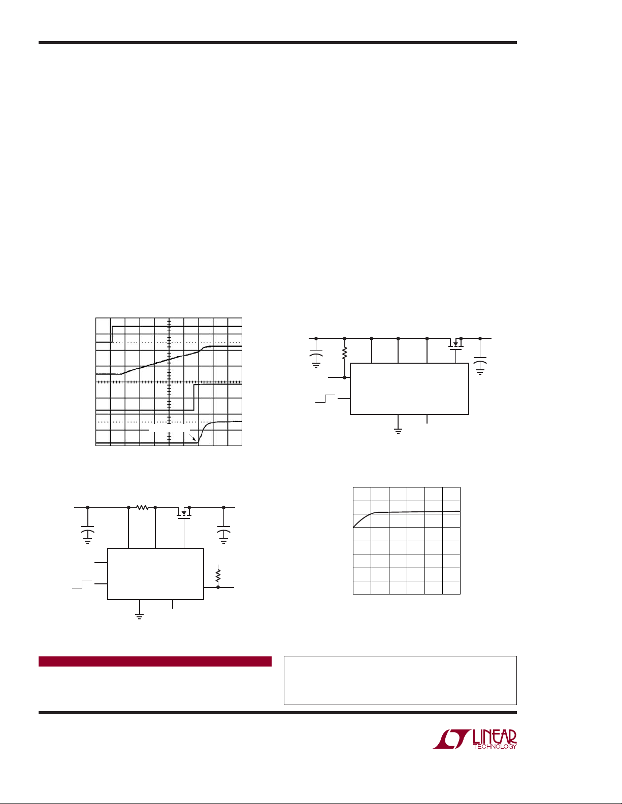
minimized. Then, 50µs after the circuit breaker is armed,
the READY pin goes high (see trace 3) and signals the
system to power up V
waveform when V
. Trace 4 shows the related V
IN
powers up. In order to not trip the
IN
OUT
circuit breaker during startup, the load current must be
lower than V
CB/RSENSE
. If needed, the I
pin can be
SEL
stepped dynamically for a higher overcurrent threshold
at startup and a lower threshold when the load current
has stabilized.
Accurate ECB with Sense Resistor
The R
voltage drop sensing method trades the
DS(ON)
circuit breaker accuracy for system simplicity. The
majority of sensing inaccuracy is due to the external
MOSFET’s R
under different V
also do not specify the R
varied by operating temperature and
DS(ON)
bias condition. The MOSFET vendors
GS
distribution tightly due
DS(ON)
to manufacturing variation. If an external tight tolerance
resistor is employed for current sensing instead, the
LTC4213 reveals it s ±10% circuit bre aker accuracy. Figure
(1)
V
ON
1V/DIV
(2)
V
GATE
5V/DIV
(3)
V
READY
2V/DIV
(4)
≈ V
V
OUT
IN
1V/DIV
Figure 2. Normal Power-Up Sequence
V
IN
1.9V
+
C
IN
100µF
V
BIAS
V
CC
5V
ONOFF
ON
R
GND
SENSE
7mΩ
SENSEN
LTC4213
VIN POWERS UP
0.1ms/DIV
Si4420BDY
GATESENSEP
I
SEL
Q1
READY
DN402 F03
DN402 F02
V
OUT
1.9V
5A
+
C
LOAD
100µF
V
IN
R4
10k
3 shows a tolerable R
resistor voltage drop and the
SENSE
LTC4213 is used for accurate ECB applications.
High Side Switch for N-Channel Logic Level
MOSFET
Logic level N-Channel MOSFET applications usually
requires a minimum gate drive voltage of 4.5V. Figure 4
shows the LTC4213 in a High Side Switch application.
The LTC4213’s internal charge pump boosts the GATE
above the logic level gate drive requirement and ensures
the MOSFET is fully enhanced for V
≥ 3V. The typical
CC
gate drive versus bias supply voltage curve is shown in
Figure 5.
Conclusion
The LTC4213 is a small package, No R
SENSE
Electronic
Circuit Breaker that is ideally suited for low voltage applications with low MOSFET insertion loss. It includes
selectable dual current level and dual response time circuit
breaker functions. The circuit breaker has wide operating
input common-mode-range from ground to V
Q1
3V TO 6V
V
IN
+
R
4
10µF
10k
SENSEP
CC
READY
LTC4213
ONOFF
ON
GND
Figure 4. High Side Switch for Logic
Level N-Channel MOSFET, V
8.0
7.5
7.0
(V)
6.5
SENSEN
6.0
– V
5.5
GATE
V
5.0
4.5
4.0
3.5 4.0 5.0
3.0
4.5
BIAS SUPPLY VOLTAGE (V)
Si4420BDY
SENSEN GATEV
I
SEL
DN402 F04
> 3V
CC
5.5
DN402 F05
.
CC
+
C
6.0
V
OUT
3V TO 6V
5A
LOAD
Figure 3. Accurate ECB with High Side Sense Resistor
Data Sheet Download
http://www.linear.com
Linear Technology Corporation
1630 McCarthy Blvd., Milpitas, CA 95035-7417
●
(408) 432-1900
FAX: (408) 434-0507 ● www.linear.com
Figure 5. Gate Drive Voltage vs Bias Supply Voltage
For applications help,
call (408) 432-1900, Ext. 2452
dn402f LT 1006 305K • PRINTED IN THE USA
© LINEAR TECHNOLOGY CORPORATION 2006
 Loading...