

Linear Technology LTC4210-2IS6, LTC4210-2CS6, LTC4210-1IS6, LTC4210-1CS6 Datasheet
FEATURES
LTC4210-1/LTC4210-2
Hot Swap Controller in
6-Lead SOT-23 Package
U
DESCRIPTIO
■
Allows Safe Board Insertion and Removal
from a Live Backplane
■
Adjustable Analog Current Limit
with Circuit Breaker
■
Fast Response Limits Peak Fault Current
■
Automatic Retry or Latch Off On Current Fault
■
Adjustable Supply Voltage Power-Up Rate
■
High Side Drive for External MOSFET Switch
■
Controls Supply Voltages from 2.7V to 16.5V
■
Undervoltage Lockout
■
Adjustable Overvoltage Protection
■
Low Profile (1mm) SOT-23 (ThinSOTTM) Package
U
APPLICATIO S
■
Hot Board Insertion
■
Electronic Circuit Breaker
■
Industrial High Side Switch/Circuit Breaker
U
TYPICAL APPLICATIO
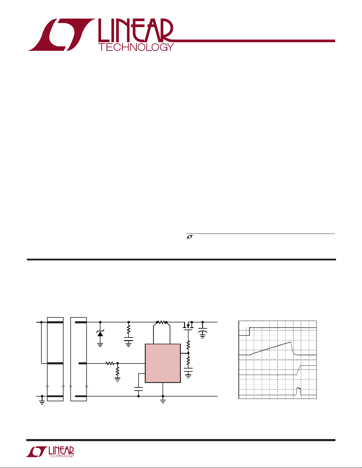
The LTC®4210 is a 6-pin SOT-23 Hot SwapTM controller
that allows a board to be safely inserted and removed from
a live backplane. An internal high side switch driver
controls the GATE of an external N-channel MOSFET for a
supply voltage ranging from 2.7V to 16.5V. The LTC4210
provides the initial timing cycle and allows the GATE to be
ramped up at an adjustable rate.
The LTC4210 features a fast current limit loop providing
active current limiting together with a circuit breaker
timer. The signal at the ON pin turns the part on and off and
is also used for the reset function.
This part is available in two options: the LTC4210-1 for
automatic retry on overcurrent fault and the LTC4210-2
for latch off on an overcurrent fault.
, LTC and LT are registered trademarks of Linear Technology Corporation.
ThinSOT and Hot Swap are trademarks of Linear Technology Corporation.
V
GND
IN
5V
BACKPLANE
CONNECTOR
(FEMALE)
Single Channel 5V Hot Swap Controller
PCB EDGE
CONNECTOR
(MALE)
LONG
R
R
10k
ON2
10Ω
X
C
X
0.1µF
Z1
OPTIONAL
R
ON1
SHORT
LONG
Z1: ISMA10A OR SMAJ10A
20k
R
0.01Ω
VCCSENSE
LTC4210
ON
TIMER
C
TIMER
0.22µF
SENSE
GND
GATE
Q1
Si4410DY
R
100Ω
R
100Ω
+
G
C
C
C
0.01µF
470µF
C
LOAD
4210 TA01
V
OUT
5V
4A
GND
Power-Up Sequence
C
= 470µF
LOAD
10ms/DIV
4210 TA02
V
ON
(2V/DIV)
V
TIMER
(1V/DIV)
V
OUT
(5V/DIV)
I
OUT
(0.5A/DIV)
421012f
1
LTC4210-1/LTC4210-2
PACKAGE/ORDER I FOR ATIO
UU
W
WWWU
ABSOLUTE AXI U RATI GS
(Note 1)
Supply Voltage (VCC) ............................................... 17V
Input Voltage (SENSE, TIMER) .. –0.3V to (VCC + 0.3V)
Input Voltage (ON)..................................... –0.3V to 17V
Output Voltage (GATE) ........ Internally Limited (Note 3)
Operating Temperature Range
LTC4210-1C/LTC4210-2C ....................... 0°C to 70°C
LTC4210-1I/LTC4210-2I .................... –40°C to 85°C
Storage Temperature Range ................. –65°C to 150°C
Lead Temperature (Soldering, 10 sec)..................300°C
ORDER PART
NUMBER
TOP VIEW
TIMER 1
GND 2
ON 3
S6 PACKAGE
6-LEAD PLASTIC TSOT-23
T
= 125°C, θJA = 230°C/ W
JMAX
6 V
CC
5 SENSE
4 GATE
LTC4210-1CS6
LTC4210-2CS6
LTC4210-1IS6
LTC4210-2IS6
S6 PART MARKING
LTYW
LTYX
LTF5
LTF6
Consult LTC Marketing for parts specified with wider operating temperature ranges.
ELECTRICAL CHARACTERISTICS
The ● denotes specifications which apply over the full operating
temperature range, otherwise specifications are TA = 25°C. VCC = 5V, unless otherwise noted. (Note 2)
SYMBOL PARAMETER CONDITIONS MIN TYP MAX UNITS
V
CC
I
CC
V
LKOR
V
LKOHYST
I
INON
I
INSENSE
V
CB
I
GATEUP
I
GATEDN
∆V
GATE
I
TIMERUP
I
TIMERDN
V
TIMER
V
TMRHYST
V
ON
V
ONHYST
Supply Voltage ● 2.7 16.5 V
VCC Supply Current ● 0.65 3.5 mA
VCC Undervoltage Lockout Release VCC Rising ● 2.2 2.5 2.65 V
VCC Undervoltage Lockout Hysteresis 100 mV
ON Pin Input Current ● –10 0 10 µA
SENSE Pin Input Current V
Circuit Breaker Trip Voltage VCB = (VCC – V
GATE Pin Pull-Up Current V
GATE Pin Pull-Down Current V
External N-Channel Gate Drive V
TIMER Pin Pull-Up Current Initial Cycle, V
TIMER Pin Pull-Down Current After Current Fault Disappears, V
TIMER Pin Threshold High Threshold, TIMER Rising ● 1.22 1.3 1.38 V
TIMER Low Threshold Hysteresis 100 mV
ON Pin Threshold ON Threshold, ON Rising ● 1.22 1.3 1.38 V
ON Pin Threshold Hysteresis 80 mV
= V
SENSE
GATE
TIMER
V
ON
VCC – V
GATE
V
GATE
V
GATE
V
GATE
V
GATE
V
GATE
During Current Fault Condition, V
Under Normal Conditions, V
Low Threshold, TIMER Falling
CC
) ● 44 50 56 mV
SENSE
= 0V ● –5 –10 –15 µA
= 1.5V, V
= 0V, V
GATE
SENSE
– VCC, VCC = 2.7V ● 4.0 6.5 8 V
– VCC, VCC = 3V ● 4.5 7.5 10 V
– VCC, VCC = 3.3V ● 5.0 8.5 12 V
– VCC, VCC = 5V ● 10 12 16 V
– VCC, VCC = 12V ● 9.0 12 16 V
– VCC, VCC = 15V ● 6.0 11 18 V
= 3V or 25 mA
GATE
= 3V or
= 100mV, V
= 1V ● –2 –5 –8.5 µA
TIMER
= 3V
GATE
TIMER
TIMER
= 1V 100 µA
TIMER
● –10 5 10 µA
= 1V ● –25 –60 –100 µA
= 1V ● 2 3.5 µA
● 0.15 0.2 0.25 V
2
421012f
LTC4210-1/LTC4210-2
ELECTRICAL CHARACTERISTICS
The ● denotes specifications which apply over the full operating
temperature range, otherwise specifications are TA = 25°C. VCC = 5V, unless otherwise noted. (Note 2)
SYMBOL PARAMETER CONDITIONS MIN TYP MAX UNITS
t
OFF(TMRHIGH)
t
OFF(ONLOW)
t
OFF(VCCLOW)
Note 1: Absolute Maximum Ratings are those values beyond which the life
of a device may be impaired.
Note 2: All currents into device pins are positive; all currents out of device
pins are negative. All voltages are referenced to ground unless otherwise
specified.
Turn-Off Time (TIMER Rise to GATE Fall) V
= 0V to 2V Step, VCC = VON = 5V 1 µs
TIMER
Turn-Off Time (ON Fall to GATE Fall) VON = 5V to 0V Step, VCC = 5V 30 µs
Turn-Off Time (VCC Fall to IC Reset) VCC = 5V to 2V Step, VON = 5V 30 µs
Note 3: An internal Zener on the GATE pin clamps the charge pump
voltage to a typical maximum voltage of 26V. External overdrive of the
GATE pin beyond the internal Zener voltage may damage the device.
Without a limiting resistor, the GATE capacitance must be <0.15µF at
maximum V
. If a lower GATE pin clamp voltage is desired, an external
CC
Zener diode may be used.
UW
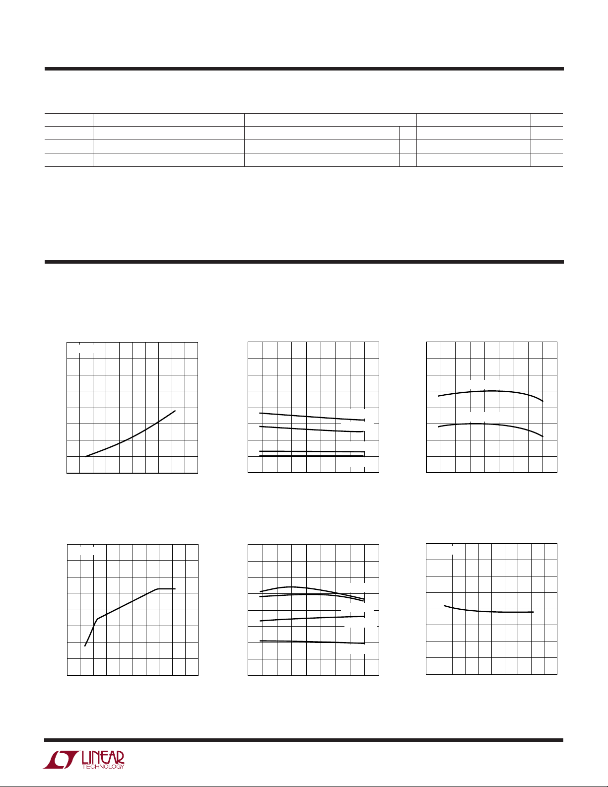
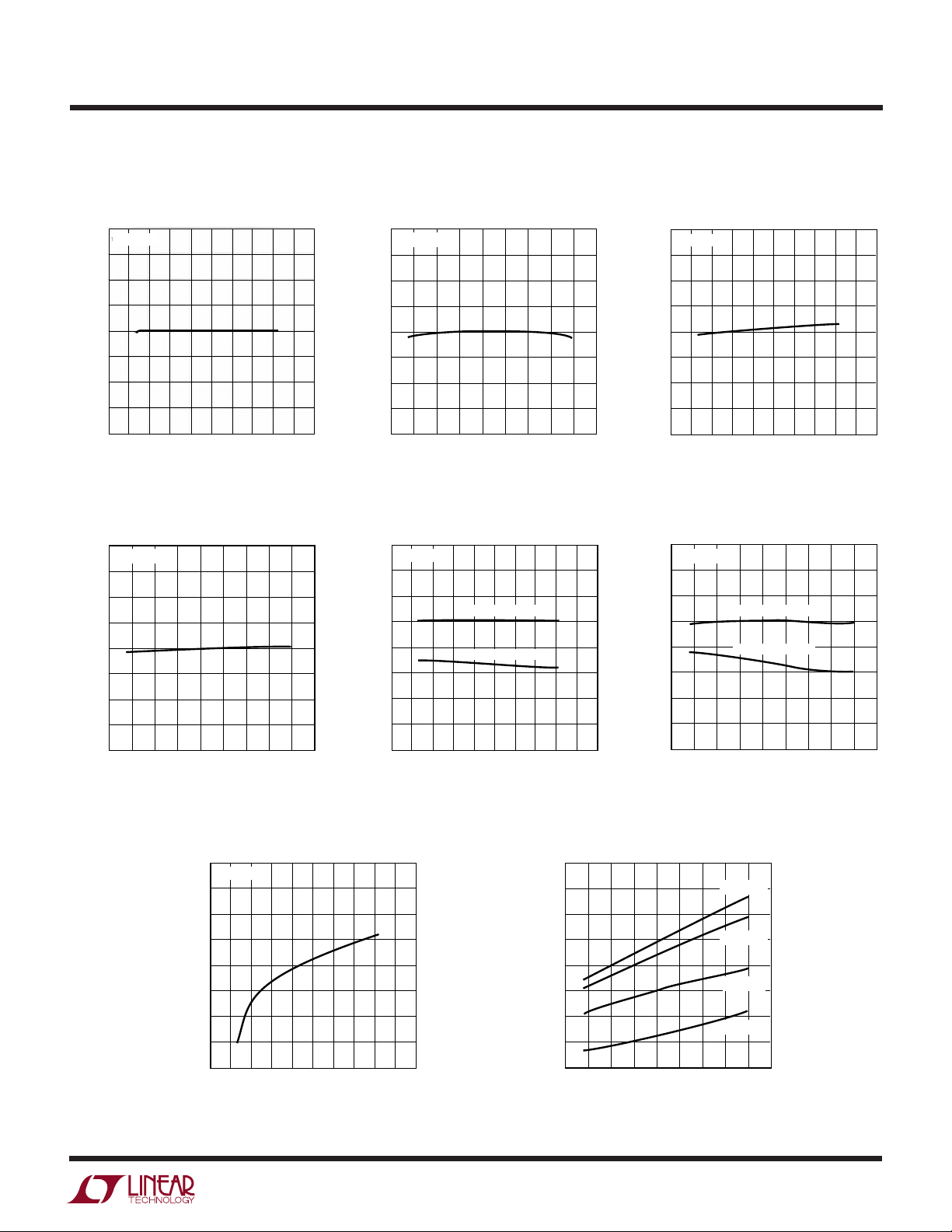
TYPICAL PERFOR A CE CHARACTERISTICS
Undervoltage Lockout Threshold
Supply Current vs Supply Voltage Supply Current vs Temperature
4.0
TA = 25°C
3.5
3.0
2.5
2.0
1.5
SUPPLY CURRENT (mA)
1.0
0.5
0
42 6 10 14 18
0
SUPPLY VOLTAGE (V)
12
16
8
20
4210 G01 4210 G02 4210 G03
4.0
3.5
3.0
2.5
2.0
1.5
SUPPLY CURRENT (mA)
1.0
0.5
0
–75
0 25 50 75 100 125
–25–50
TEMPERATURE (°C)
VCC = 15V
VCC = 12V
VCC = 5V
VCC = 3V
150
vs Temperature
2.65
2.60
2.55
2.50
2.45
2.40
2.35
2.30
UNDERVOLTAGE LOCKOUT THRESHOLD (V)
2.25
–75
VCC RISING
VCC FALLING
0 25 50 75 100 125
–25–50
TEMPERATURE (°C)
150
(V)
GATE
V
40
35
30
25
20
15
10
5
0
V
vs Supply Voltage V
GATE
TA = 25°C
42 6 10 14 18
0
SUPPLY VOLTAGE (V)
12
16
8
20
4210 G04 4210 G05 4210 G06
(V)
GATE
V
vs Temperature
GATE
40
35
30
25
20
15
10
5
0
–75
0 25 50 75 100 125
–25–50
TEMPERATURE (°C)
VCC = 15V
VCC = 12V
VCC = 5V
VCC = 3V
150
–8.0
–8.5
–9.0
–9.5
(µA)
–10.0
GATEUP
I
–10.5
–11.0
–11.5
–12.0
I
vs Supply Voltage
GATEUP
TA = 25°C
42 6 10 14 18
0
8
SUPPLY VOLTAGE (V)
12
16
20
421012f
3
LTC4210-1/LTC4210-2
UW
TYPICAL PERFOR A CE CHARACTERISTICS
∆V
vs Supply Voltage
GATE
TA = 25°C
42 6 10 14 18
0
8
SUPPLY VOLTAGE (V)
12
16
–8.0
–8.5
–9.0
–9.5
(µA)
–10.0
GATEUP
I
–10.5
–11.0
–11.5
–12.0
I
GATEUP
–75
vs Temperature
VCC = 3V
VCC = 15V
0 25 50 75 100 125
–25–50
TEMPERATURE (°C)
VCC = 12V
VCC = 5V
4210 G07
150
(V)
GATE
∆V
18
16
14
12
10
8
6
4
2
4210 G08
∆V
vs Temperature
GATE
18
16
14
12
(V)
10
GATE
∆V
8
6
4
2
20
–75 150
0 25 50 75 100 125
–25–50
TEMPERATURE (°C)
VCC = 5V
VCC = 12V
VCC = 15V
VCC = 3V
4210 G09
I
(In Initial Cycle)
TIMERUP
vs Supply Voltage
0
TA = 25°C
–1
–2
–3
–4
(µA)
–5
–6
TIMERUP
I
–7
–8
–9
–10
42 6 10 14 18
0
I
TIMERUP
8
SUPPLY VOLTAGE (V)
(During Circuit Breaker
12
16
Delay) vs Temperature
–20
VCC = 5V
–30
–40
–50
(µA)
–60
TIMERUP
I
–70
–80
–90
–100
–75 150
0 25 50 75 100 125
–25–50
TEMPERATURE (°C)
I
vs Temperature
0
–1
–2
–3
–4
(µA)
–5
–6
TIMERUP
I
–7
–8
–9
–10
20
4210 G10 4210 G11 4210 G12
–75 150
I
vs Supply Voltage
3.0
2.8
2.6
2.4
2.2
(µA)
2.0
1.8
TIMERDN
I
1.6
1.4
1.2
1.0
0
4210 G13
(In Initial Cycle)
TIMERUP
VCC = 5V
0 25 50 75 100 125
–25–50
TEMPERATURE (°C)
(In Cool-Off Cycle)
TIMERDN
TA = 25°C
42 6 10 14 18
8
SUPPLY VOLTAGE (V)
I
(During Circuit Breaker
TIMERUP
Delay) vs Supply Voltage
–20
TA = 25°C
–30
–40
–50
(µA)
–60
TIMERUP
I
–70
–80
–90
–100
42 6 10 14 18
0
I
TIMERDN
8
SUPPLY VOLTAGE (V)
(In Cool-Off Cycle)
12
16
vs Temperature
3.0
VCC = 5V
2.8
2.6
2.4
2.2
(µA)
2.0
1.8
TIMERDN
I
1.6
1.4
1.2
1.0
12
16
20
4210 G14
–75 150
0 25 50 75 100 125
–25–50
TEMPERATURE (°C)
4210 G15
20
4
421012f
UW
TYPICAL PERFOR A CE CHARACTERISTICS
LTC4210-1/LTC4210-2
TIMER High Threshold
vs Supply Voltage
1.38
TA = 25°C
1.36
1.34
1.32
1.30
1.28
1.26
TIMER HIGH THRESHOLD (V)
1.24
1.22
42 6 10 14 18
0
8
SUPPLY VOLTAGE (V)
12
16
20
4210 G16
TIMER Low Threshold
vs Temperature
0.24
VCC = 5V VCC = 5V
0.23
0.22
0.21
0.20
0.19
0.18
TIMER LOW THRESHOLD (V)
0.17
0.16
–75 150
0 25 50 75 100 125
–25–50
TEMPERATURE (°C)
4210 G19
TIMER High Threshold
vs Temperature
1.38
VCC = 5V
1.36
1.34
1.32
1.30
1.28
1.26
TIMER HIGH THRESHOLD (V)
1.24
1.22
–75 150
0 25 50 75 100 125
–25–50
TEMPERATURE (°C)
ON Pin Threshold
vs Supply Voltage
1.45
TA = 25°C
1.40
1.35
1.30
1.25
1.20
ON PIN THRESHOLD (V)
1.15
1.10
1.05
0
HIGH THRESHOLD
LOW THRESHOLD
42 6 10 14 18
SUPPLY VOLTAGE (V)
12
8
4210 G17
16
20
4210 G20
TIMER Low Threshold
vs Supply Voltage
0.24
TA = 25°C
0.23
0.22
0.21
0.20
0.19
0.18
TIMER LOW THRESHOLD (V)
0.17
0.16
42 6 10 14 18
0
8
SUPPLY VOLTAGE (V)
12
ON Pin Threshold
vs Temperature
1.45
1.40
1.35
1.30
1.25
1.20
ON PIN THRESHOLD (V)
1.15
1.10
1.05
–75 150
HIGH THRESHOLD
LOW THRESHOLD
0 25 50 75 100 125
–25–50
TEMPERATURE (°C)
16
20
4210 G18
4210 G21
t
OFF(ONLOW)
80
TA = 25°C
70
60
50
(µs)
40
30
OFF,ONLOW
t
20
10
0
016
vs Supply Voltage
42 6 10 14 18
SUPPLY VOLTAGE (V)
12
8
20
4210 G22
t
OFF(ONLOW)
80
70
60
50
(µs)
40
30
OFF,ONLOW
t
20
10
0
–75 150
vs Temperature
0 25 50 75 100 125
–25–50
TEMPERATURE (°C)
VCC = 15V
VCC = 12V
VCC = 5V
VCC = 3V
4210 G23
421012f
5
LTC4210-1/LTC4210-2
UW
TYPICAL PERFOR A CE CHARACTERISTICS
VCB vs Supply Voltage
58
TA = 25°C
56
54
52
(mV)
50
CB
V
48
46
44
42
U
42 6 10 14 18
0
8
SUPPLY VOLTAGE (V)
UU
12
16
20
4210 G24
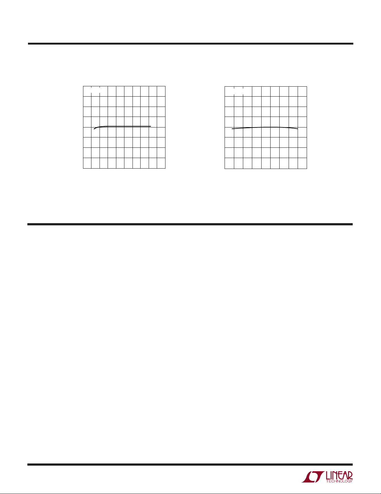
PI FU CTIO S
TIMER (Pin 1): Timer Input Pin. An external capacitor
C
µF circuit breaker delay. The GATE pin turns off whenever
the TIMER pin is pulled beyond the COMP2 threshold,
such as for overvoltage detection with an external zener.
GND (Pin 2): Ground Pin.
ON (Pin 3): ON Input Pin. The ON pin comparator has a
low-to-high threshold of 1.3V with 80mV hysteresis and a
glitch filter. When the ON pin is low, the LTC4210 is reset.
When the ON pin goes high, the GATE turns on after the
initial timing cycle.
GATE (Pin 4): GATE Output Pin. This pin is the high side
gate drive of an external N-channel MOSFET. An internal
charge pump provides a 10µA pull-up current with Zener
clamps to VCC and ground. In overload, the error amplifier
sets a 272.9ms/µF initial timing delay and a 21.7ms/
TIMER
VCB vs Temperature
58
VCC = 5V
56
54
52
(mV)
50
CB
V
48
46
44
42
–75 150
0 25 50 75 100 125
–25–50
TEMPERATURE (°C)
4210 G25
(EA) controls the external MOSFET to maintain a constant
load current. An external R-C compensation network
should be connected to this pin for current limit loop
stability.
SENSE (Pin 5): Current Limit Sense Input Pin. A sense
resistor between the VCC and SENSE pins sets the analog
current limit. In overload, the EA controls the external
MOSFET gate to maintain the SENSE pin voltage at 50mV
below VCC. When the EA is maintaining current limit, the
TIMER circuit breaker mode is activated. The current limit
loop/circuit breaker mode can be disabled by connecting
the SENSE pin to the VCC pin.
VCC (Pin 6): Positive Supply Input Pin. The operating
supply voltage range is between 2.7V to 16.5V. An undervoltage lockout (UVLO) circuit with a glitch filter resets the
LTC4210 when a low supply voltage is detected.
6
421012f
 Loading...