

Complete Battery Charger Solution for High Current Portable
Electronics
3.5A Charger for Li-Ion/LiFePO4 Batteries Multiplexes USB and Wall Inputs
Design Note 496
George H. Barbehenn
Introduction
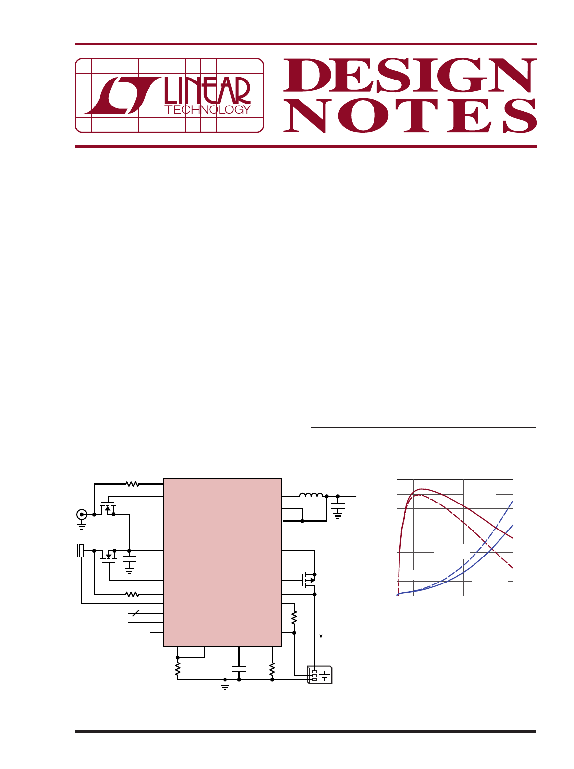
The LTC®4155 and LTC4156 are dual multiplexed-input
battery chargers with PowerPath™ control, featuring I
2
C
programmability and USB On-The-Go for systems such
as tablet PCs and other high power density applications.
The LTC4155’s float voltage (V
) range is optimized
FLOAT
for Li-Ion batteries, while the LTC4156 is optimized for
lithium iron phosphate (LiFePO
) batteries, supporting
4
system loads to 4A with up to 3.5A of battery charge
current. I
2
C controls a broad range of functions and USB
On-The-Go functionality is controlled directly from the
USB connector ID pin.
Input Multiplexer
A distinctive feature of the LTC4155/LTC4156 PowerPath
implementation is a dual-input multiplexer using only
R2, 3.6k
WALL
MN2
USB
MN1
R1, 3.6k
TO µC
TO µC
L1: COILCRAFT XFL4020-102ME
MN1: Si4430BDY
MP1: VISHAY Si5481DU-T1-GE3
23, 24, 25
C3
10µF
3
1, 2, 28
7
WALLSNS
11
WALLGT
LTC4155/LTC4156
V
BUS
9
USBGT
8
USBSNS
4
ID NTCBIAS
2
C
I
3
IRQ
10
OVGCAP
CLPROG1 CLPROG2 GND PROGV
5 6 29 12 18
R3
1.21k
C
V
CHGSNS
BATGATE
BATSNS
C1
0.047µF
SW
OUTSNS
V
OUT
NTC
R4
665Ω
26, 27
13
21, 22
19, 20
17
16
14
15
N-channel MOSFETs controlled by an internal charge
pump. The input multiplexer has input priority selection
and independent input current limits for each channel.
Applications include any device with a high capacity
Li-Ion or LiFePO
battery that can be charged from a high
4
current wall adapter input or from the USB input—such
as a tablet PC. Figure 1 shows a typical application and
Figure 2 shows its efficiency.
This dual input multiplexer implementation allows the
use of inexpensive, low R
N-channel MOSFETs.
DS(ON)
The MOSFETs also provide overvoltage protection (OVP)
and if desired, backdrive blocking and reverse-voltage
L, LT, LTC, LTM, Linear Technology, the Linear logo are registered trademarks and
PowerPath is a trademark of Linear Technology Corporation. All other trademarks are
the property of their respective owners.
95.0
92.5
90.0
87.5
85.0
82.5
EFFICIENCY (%)
80.0
77.5
75.0
INCLUDES LOSSES FROM 2× Si7938DP OVP FETS
XFL4020-102ME INDUCTOR AND Si5481DU CHARGER FET
EFFICIENCY
TO BATTERY
POWER LOST
V
= 3.7V
BATSNS
0.50 1.0 2.0
TO BATTERY
1.5
CURRENT (A)
EFFICIENCY
TO V
OUT
POWER LOST
TO V
OUT
2.5 3.0 3.5
DN4GB F02
Figure 2. Switching Regulator Efficiency
R5
80k
1µH
L1
MP1
1.8A
LIMIT
TO SYSTEM
LOAD
C2
22µF
DN4GB F01
4.0
3.5
3.0
POWER LOST (W)
2.5
2.0
1.5
1.0
0.5
0
11/11/496
Figure 1. Typical Application Using a Simple Input
Multiplexer with No Backdrive Protection
protection (RVP). Backdrive blocking prevents voltage on
+
the wall input from backdriving the USB, or vice-versa.
Backdrive blocking can be implemented on one or both
inputs. Reverse-voltage protection prevents a negative
voltage applied to the protected input from reaching
downstream circuits.
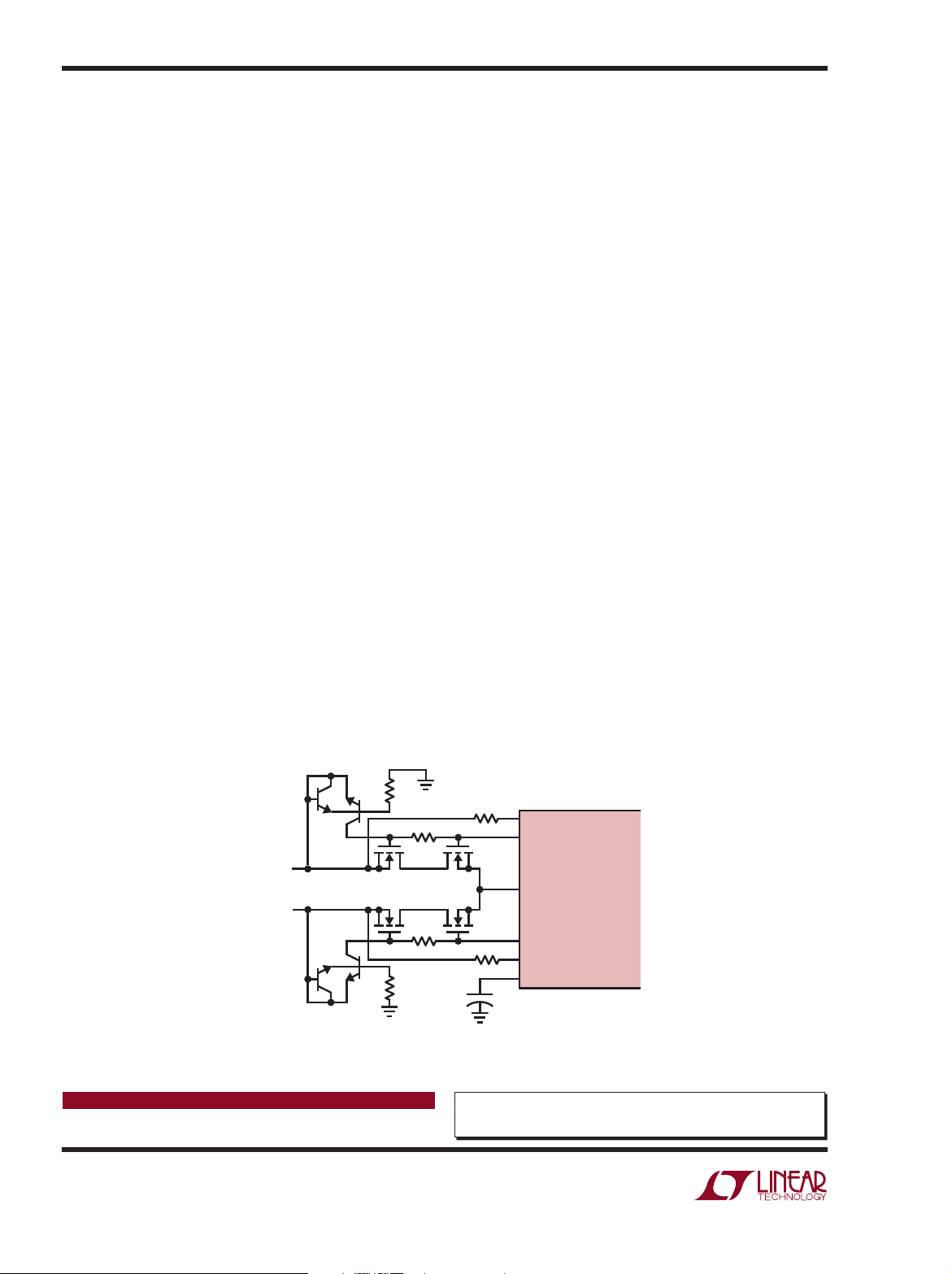
Dual High Current Input Application
Figure 3 shows a dual 3.5A inpu t application, featuring OV P,
RVP and backdrive protection. The FDMC8030 MOSFETs
provide ±40V of OVP and RVP protection.
0V~6V Input on Either WALL or USB
In the circuit of Figure 3, when a 0V~6V input is present on either input, the corresponding gate signal rises
to approximately twice V
N-channel MOSFETS and connecting the input to V
, enabling the two series
IN
BUS
The undervoltage lockout (UVLO) is approximately 4.35V
on each channel.
The LTC4155/LTC4156 have an input priority bit, which
defaults to WALL. If a valid voltage is present on both
inputs, only WALLGT is activated. The input priority bit
can be change d via I
2
C to make the USB channel pre ferred
when both inputs are present.
>6V Input on Either WALL or USB
When either input goes above 6V, the corresponding
WALLGT or USBGT pin is pulled low, shutting off the
corresponding MOSFETs and disconnecting the input. If
both inputs have 5V on them, and the input that is enabled
by the input priority bit goes above 6V, the LTC4155/
LTC4156 automatically and seamlessly switches to the
other input—with no disturbance on V
OUT
.
The diode-connected NPNs (Q3 and Q4) serve to prevent
excess V
on the MOSFET closest to the input of the
GS
corresponding channel current from the input flows
through the diode, through the B-C junction of the NPN
bipolar transistor, and pulls the gate up through the 5M
resistor. This prevents the gate from dropping below the
source by more than 2V.
A voltage greater than 6V on one input does not prevent
the other input from operating normally.
< 0V Input on Either WALL or USB
The USBSNS and WALLSNS pins ignore any negative
inputs, but clamp the pins to –V
(about –0.6V). The
F
negative voltage forward-biases the base-emitter junction of the NPN bipolar transistor, shorting the gate to
.
the input and ensuring that the gate is never more than
about 0.5V above the source.
A negative voltage on one input does not prevent the
other input from operating normally.
OTG 0peration
The LTC4155/LTC4156 drive the USBGT pin high when
USB On-The-Go operation is enabled, connecting V
the USB input and enabling up to 500mA to be sourced.
Conclusion
The LTC4155/LTC4156 implement an overvoltage and
reverse-voltage protected, prioritized input multiplexer
for products that need to support multiple system power
or battery charging functionality. Optional backdrive
blocking prevents the appearance of voltages at an
unconnected input.
BUS
to
Q1
Q2
MN1A
MN2A
R5
47k
R3, 5M
R6
47k
R4 5M
MN1B
MN2B
R1 3.6k
R2 3.6k
C1
OPT
0.01µF
WALLSNS
WALLGT
LTC4155/LTC4156
V
BUS
USBGT
USBSNS
OVGCAP
DN4GB F03
Q3
TO WALL
INPUT
TO USB
INPUT
Q4
MN1, MN2 = FDMC8030
Figure 3. LTC4155/LTC4156 Input Multiplexer with OVP, RVP and Backdrive Blocking
Data Sheet Download
www.linear.com
For applications help,
call (978) 656-4700, Ext. 3752
dn496 LT/AP 1111 196K • PRINTED IN THE USA
Linear Technology Corporation
1630 McCarthy Blvd., Milpitas, CA 95035-7417
(408) 432-1900
●
FAX: (408) 434-0507 ● www.linear.com
LINEAR TECHNOLOGY CORPORATION 2011
 Loading...