

LTC4090/LTC4090-5
USB Power Manager with
2A High Voltage Bat-Track
Buck Regulator
FEATURES
■
Seamless Transition Between Power Sources: Li-
Ion Battery, USB, and 6V to 36V Supply (60V Max)
■
2A Output High Voltage Buck Regulator with Bat-
TM
Track
■
Internal 215mΩ Ideal Diode Plus Optional External
Adaptive Output Control (LTC4090)
Ideal Diode Controller Provides Low Loss Power
Path When External Supply / USB Not Present
■
Load Dependent Charging from USB Input Guaran-
tees Current Compliance
■
Full Featured Li-Ion Battery Charger
■
1.5A Maximum Charge Current with Thermal Limiting
■
NTC Thermistor Input for Temperature Qualifi ed
Charging
■
Tiny (3mm × 6mm × 0.75mm) 22-Pin DFN Package
APPLICATIONS
■
HDD-Based Media Players
■
Personal Navigation Devices
■
Other USB-Based Handheld Products
■
Automotive Accessories
DESCRIPTION
The LTC®4090/LTC4090-5 are USB power managers plus
high voltage Li-Ion/Polymer battery chargers. The devices
control the total current used by the USB peripheral for
operation and battery charging. Battery charge current is
automatically reduced such that the sum of the load current
and the charge current does not exceed the programmed
input current limit. The LTC4090/LTC4090-5 also accommodate high voltage power supplies, such as 12V AC/DC
wall adapters, FireWire, or automotive power.
The LTC4090 provides a Bat-Track adaptive output that
tracks the battery voltage for high effi ciency charging from
the high voltage input. The LTC4090-5 provides a fi xed 5V
output from the high voltage input to charge single cell
Li-Ion bateries. The charge current is programmable and an
⎯C⎯H⎯R⎯
end-of-charge status output (
Also featured are programmable total charge time, an NTC
thermistor input used to monitor battery temperature while
charging and automatic recharging of the battery.
, LT, LTC and LTM are registered trademarks of Linear Technology Corporation.
Bat-Track is a trademark of Linear Technology Corporation. All other trademarks are the
property of their respective owners.
G) indicates full charge.
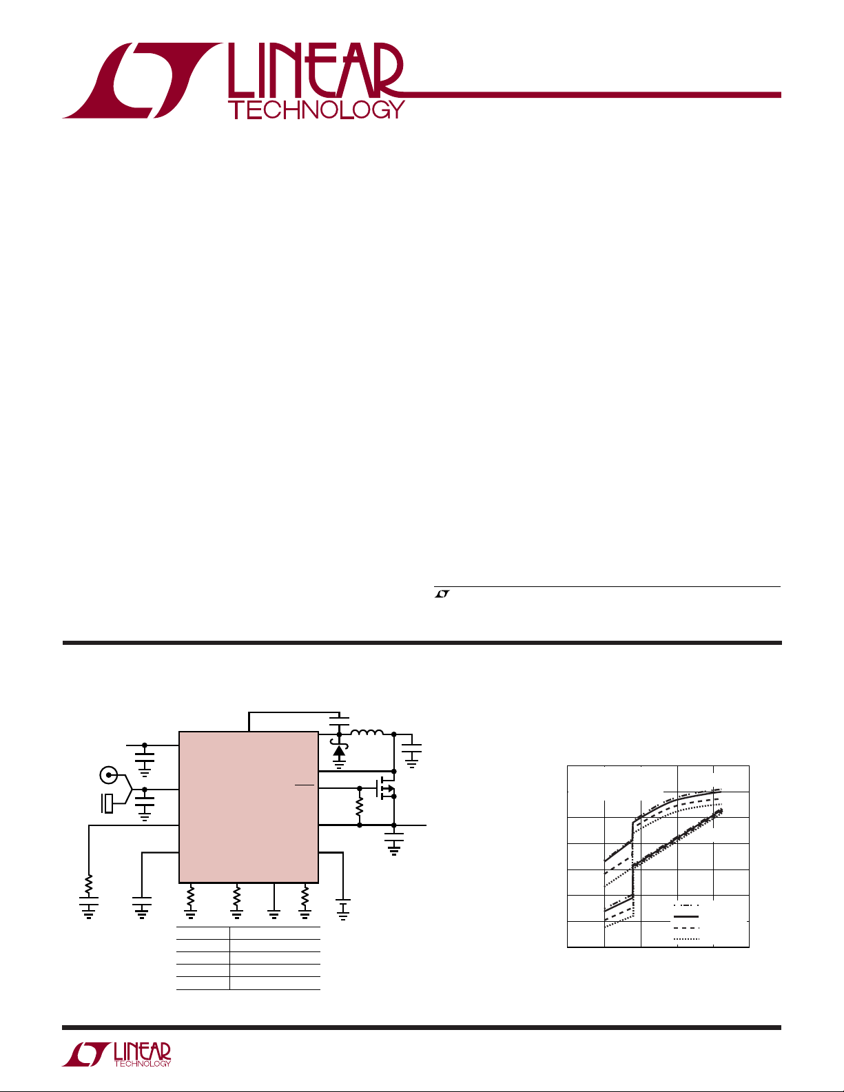
TYPICAL APPLICATION
CLPROG
40.2k
(TYP)
+ 0.3V
5V
5V
BAT
BOOST
LTC4090
GND PROG
AVAILABLE INPUT
HV INPUT (LTC4090)
HV INPUT (LTC4090-5)
USB ONLY
BAT ONLY
HIGH (6V-36V)
VOLTAGE INPUT
5V WALL
ADAPTER
USB
59k
270pF
1μF
4.7μF
0.1μF
HVIN
IN
V
C
TIMER
R
T
V
OUT
V
BAT
V
0.47μF
SW
HVOUT
HVPR
OUT
BAT
6.8μH
22μF
1k
LOAD
4.7μF
+
100k2k
Li-Ion BATTERY
4090 TAO1
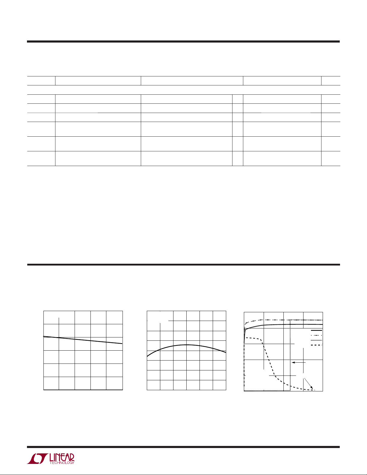
LTC4090/LTC4090-5 High Voltage
Battery Charger Effi ciency
90
FIGURE 12 SCHEMATIC
WITH R
80
NO OUTPUT LOAD
70
60
50
EFFICIENCY (%)
40
30
20
2.0
PROG
2.5
= 52k
3.0
V
BAT
LTC4090
3.5
(V)
LTC4090-5
HVIN = 8V
HVIN = 12V
HVIN = 24V
HVIN = 36V
4.0
4090 TA01b
4.5
4090fa
1
LTC4090/LTC4090-5
(Notes 1, 2, 3, 4)
HVIN, HVEN (Note 9) ................................................60V
BOOST ......................................................................56V
BOOST above SW .....................................................30V
PG, SYNC ..................................................................30V
IN, OUT, HVOUT
t < 1ms and Duty Cycle < 1% .................. –0.3V to 7V
Steady State ............................................. –0.3V to 6V
BAT, HPWR, SUSP, V
NTC, TIMER, PROG, CLPROG ..........–0.3V to V
, I
, I
I
IN
OUT
(Note 5) ..............................................2.5A
BAT
Operating Temperature Range .....................–40 to 85°C
Junction Temperature ........................................... 110°C
Storage Temperature Range .......................–65 to 125°C
, ⎯C⎯H⎯R⎯G, ⎯H⎯V⎯P⎯R ........... –0.3V to 6V
C
+ 0.3V
CC
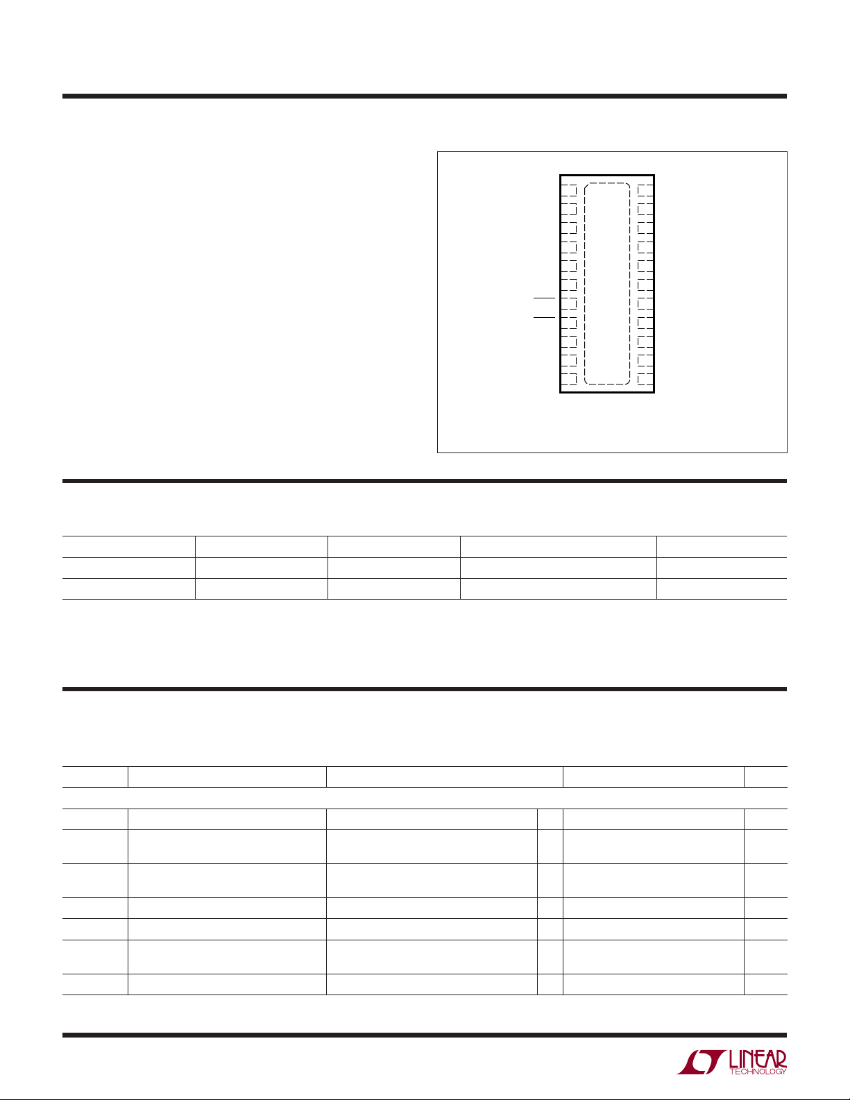
PIN CONFIGURATIONABSOLUTE MAXIMUM RATINGS
TOP VIEW
SYNC
1
PG
2
R
3
T
V
4
C
NTC
5
VNTC
6
HVPR
7
CHRG
8
PROG
9
GATE
10
BAT
11
22-LEAD (6mm × 3mm) PLASTIC DFN
EXPOSED PAD (PIN 23) IS GND, MUST BE SOLDERED TO PCB
DJC PACKAGE
T
= 110°C, θJA = 47°C/W
JMAX
22
HVEN
21
HVIN
20
SW
19
BOOST
18
HVOUT
23
17
TIMER
16
SUSP
15
HPWR
14
CLPROG
13
OUT
12
IN
ORDER INFORMATION
LEAD FREE FINISH TAPE AND REEL PART MARKING PACKAGE DESCRIPTION TEMPERATURE RANGE
LTC4090EDJC#PBF LTC4090EDJC#TRPBF 4090 22-Lead (6mm × 3mm) Plastic DFN –40°C to 85°C
LTC4090EDJC-5#PBF LTC4090EDJC-5#TRPBF 40905 22-Lead (6mm × 3mm) Plastic DFN –40°C to 85°C
Consult LTC Marketing for parts specifi ed with wider operating temperature ranges.
Consult LTC Marketing for information on non-standard lead based fi nish parts.
For more information on lead free part marking, go to: http://www.linear.com/leadfree/
For more information on tape and reel specifi cations, go to: http://www.linear.com/tapeandreel/
ELECTRICAL CHARACTERISTICS
The ● denotes the specifi cations which apply over the full operating
temperature range, otherwise specifi cations are at TA = 25°C. HVIN = HVEN = 12V, BOOST = 17V, VIN = HPWR = 5V, V
R
= 100k, R
PROG
SYMBOL PARAMETER CONDITIONS MIN TYP MAX UNITS
USB Input Current Limit
V
IN
I
IN
I
LIM
I
IN(MAX)
R
ON
V
CLPROG
I
SS
USB Input Supply Voltage
Input Bias Current I
Current Limit HPWR = 5V
Maximum Input Current Limit (Note 7) 2.4 A
On-Resistance VIN to V
CLPROG Servo Voltage in Current Limit R
Soft-Start Inrush Current 10 mA/μs
= 2k and SUSP = 0V, unless otherwise noted.
CLPROG
= 0 (Note 6)
BAT
Suspend Mode; SUSP = 5V
HPWR = 0V
I
OUT
= 80mA 0.215
OUT
CLPROG
R
CLPROG
= 2k
= 1k
●
4.35 5.5 V
●
●
●
475
●
90
●
0.98
●
0.98
0.5
50
500
100
1.00
1.00
BAT
= 3.7V,
1
100
525
110
1.02
1.02
mA
μA
mA
mA
Ω
V
V
2
4090fa
LTC4090/LTC4090-5
ELECTRICAL CHARACTERISTICS
The ● denotes the specifi cations which apply over the full operating
temperature range, otherwise specifi cations are at T
R
PROG
= 100k, R
= 2k and SUSP = 0V, unless otherwise noted.
CLPROG
= 25°C. HVIN = HVEN = 12V, BOOST = 17V, VIN = HPWR = 5V, V
A
SYMBOL PARAMETER CONDITIONS MIN TYP MAX UNITS
V
V
ΔV
CLEN
UVLO
UVLO
Input Current Limit Enable Threshold
Voltage (V
- V
OUT
)
IN
Input Undervoltage Lockout VIN Rising
Input Undervoltage Lockout Hysteresis VIN Rising – VIN Falling 130 mV
(V
(V
- V
) Rising
IN
OUT
- V
) Falling
IN
OUT
20
–80
●
3.6 3.8 4 V
50
–50
High Voltage Regulator
V
V
I
HVIN
V
V
HVIN
OVLO
OUT
OUT
HVIN Supply Voltage
HVIN Overvoltage Lockout Threshold
HVIN Bias Current Shutdown; HVEN = 0.2V
Not Switching, HVOUT = 3.6V
Output Voltage with HVIN Present Assumes HVOUT to OUT Connection,
0 ≤ V
≤ 4.2V (LTC4090)
BAT
Output Voltage with HVIN Present Assumes HVOUT to OUT Connection
●
660V
●
36 41.5 45 V
0.01
●
3.45 V
130
+ 0.3 4.6 V
BAT
4.85 5 5.15 V
(LTC4090-5)
f
SW
t
OFF
I
SW(MAX)
V
SAT
I
R
V
B(MIN)
I
BST
Switching Frequency RT = 8.66k
R
= 29.4k
T
R
= 187k
T
Minimum Switch Off-Time
2.1
0.9
160
●
2.4
1.0
200
60 150 ns
Switch Current Limit Duty Cycle = 5% 3.0 3.5 4.0 A
Switch V
CESAT
ISW = 2A 500 mV
Boost Schottky Reverse Leakage SW = 10V, HVOUT = 0V 0.02 2 μA
Minimum Boost Voltage (Note 8)
●
1.5 2.1 V
BOOST Pin Current ISW = 1A 22 35 mA
Battery Management
I
BAT
V
FLOAT
I
CHG
I
CHG(MAX)
V
PROG
k
EOC
Battery Drain Current V
= 4.3V, Charging Stopped
BAT
Suspend Mode, SUSP = 5V
V
= 0V, BAT Powers OUT, No Load
IN
V
Regulated Output Voltage I
BAT
Constant-Current Mode Charge Current,
No Load
= 2mA
BAT
I
= 2mA; 0 ≤ TA ≤ 85°C
BAT
R
= 100k
PROG
R
= 50k, 0 ≤ TA ≤ 85°C
PROG
Maximum Charge Current 1.5 A
PROG Pin Servo Voltage R
Ratio of End-of-Charge Indication
R
V
PROG
PROG
BAT
= 100k
= 50k
= V
FLOAT
(4.2V)
●
●
●
4.165
4.158
●
465
900
●
0.98
●
0.98
●
0.085 0.1 0.11 mA/mA
15
22
60
4.200
4.200
500
1000
1.00
1.00
Current to Charge Current
I
TRKL
V
TRKL
V
CEN
ΔV
RECHRG
Trickle Charge Current BAT = 2V 35 50 60 mA
Trickle Charge Threshold Voltage BAT Rising
Charge Enable Threshold Voltage (V
(V
OUT
OUT
– V
– V
) Falling; V
BAT
) Rising; V
BAT
BAT
BAT
= 4V
= 4V
Recharge Battery Threshold Voltage Threshold Voltage Relative to V
FLOAT
●
2.75 2.9 3.0 V
55
80
●
–65 –100 –135 mV
BAT
= 3.7V,
80
–20
0.5
200
2.7
1.15
240
27
35
100
4.235
4.242
535
1080
1.02
1.02
mV
mV
MHz
MHz
kHz
mA
mA
mV
mV
μA
μA
μA
μA
μA
V
V
V
V
4090fa
3
LTC4090/LTC4090-5
ELECTRICAL CHARACTERISTICS
The ● denotes the specifi cations which apply over the full operating
temperature range, otherwise specifi cations are at T
R
PROG
= 100k, R
= 2k and SUSP = 0V, unless otherwise noted.
CLPROG
= 25°C. HVIN = HVEN = 12V, BOOST = 17V, VIN = HPWR = 5V, V
A
SYMBOL PARAMETER CONDITIONS MIN TYP MAX UNITS
t
TIMER
TIMER Accuracy V
= 4.3V –10 10 %
BAT
Recharge Time Percent of Total Charge Time 50 %
Low Battery Trickle Charge Time Percent of Total Charge Time,
<2.9V
V
BAT
T
LIM
Junction Temperature in Constant
25 %
105 °C
Temperature Mode
Internal Ideal Diode
R
FWD
R
DIO, ON
V
FWD
V
OFF
I
FWD
I
D(MAX)
Incremental Resistance, VON Regulation I
On-Resistance V
Voltage Forward Drop (V
BAT
to V
OUT
BAT
– V
OUT
)I
Diode Disable Battery Voltage 2.7 V
Load Current Limit for VON Regulation 550 mA
Diode Current Limit 2.2 A
= 100mA 125 mΩ
OUT
I
= 600mA 215 mΩ
OUT
●
10 30
55
160
I
I
OUT
OUT
OUT
= 5mA
= 100mA
= 600mA
External Ideal Diode
V
FWD, EXT
Logic (
V
CHG, SD
External Diode Forward Voltage 20 mV
⎯C⎯H⎯R⎯
G, ⎯H⎯V⎯P⎯R, TIMER, SUSP, HPWR, HVEN, PG, SYNC)
Charger Shutdown Threshold Voltage
●
0.14 0.4 V
on TIMER
I
CHG, SD
Charger Shutdown Pull-Up Current on
V
TIMER
= 0V
●
514 μA
TIMER
V
OL
V
IH
V
IL
V
HVEN, H
V
HVEN, L
I
PULLDN
I
HVEN
V
PG
ΔV
PG
I
PGLK
I
PG
V
SYNC, L
V
SYNC, H
I
SYNC
Output Low Voltage (⎯C⎯H⎯R⎯G, ⎯H⎯V⎯P⎯R); I
SINK
= 5mA
Input High Voltage SUSP, HPWR 1.2 V
Input Low Voltage SUSP, HPWR 0.4 V
HVEN High Threshold 2.3 V
HVEN Low Threshold 0.3 V
Logic Input Pull-Down Current SUSP, HPWR 2 μA
HVEN Pin Bias Current HVEN = 2.5V 5 10 μA
PG Threshold HVOUT Rising 2.8 V
PG Hysteresis 35 mV
PG Leakage PG = 5V 0.1 1 μA
PG Sink Current PG = 0.4V
SYNC Low Threshold 0.5 V
SYNC High Threshold 0.8 V
SYNC Pin Bias Current V
= 0V 0.1 μA
SYNC
●
●
100 900 μA
0.1 0.4 V
= 3.7V,
BAT
50 mV
mV
mV
4
4090fa
LTC4090/LTC4090-5
ELECTRICAL CHARACTERISTICS
The ● denotes the specifi cations which apply over the full operating
temperature range, otherwise specifi cations are at T
R
PROG
= 100k, R
= 2k and SUSP = 0V, unless otherwise noted.
CLPROG
= 25°C. HVIN = HVEN = 12V, BOOST = 17V, VIN = HPWR = 5V, V
A
SYMBOL PARAMETER CONDITIONS MIN TYP MAX UNITS
NTC
I
VNTC
V
VNTC
I
NTC
V
COLD
V
HOT
V
DIS
VNTC Pin Current VNTC = 2.5V
VNTC Bias Voltage I
VNTC
= 500μA
NTC Input Leakage Current NTC = 1V 0 ±1 μA
Cold Temperature Fault Threshold
Voltage
Hot Temperature Fault Threshold
Voltage
Rising NTC Voltage
Hysteresis
Falling NTC Voltage
Hysteresis
NTC Disable Threshold Voltage Falling NTC Voltage
Hysteresis
Note 1: Stresses beyond those listed under Absolute Maximum Ratings
may cause permanent damage to the device. Exposure to any Absolute
Maximum Rating condition for extended periods may affect device
reliability and lifetime.
Note 2: The LTC4090/LTC4090-5 are guaranteed to meet performance
specifi cations from 0°C to 85°C. Specifi cations over the –40°C to 85°C
operating temperature range are assured by design, characterization and
correlation with statistical process controls.
Note 3: This IC includes overtemperature protection that is intended
to protect the device during momentary overload conditions. Junction
temperatures will exceed 110°C when overtemperature protection is
Note 4: V
is the greater of VIN, V
CC
Note 5: Guaranteed by long term current density limitations.
Note 6: Total input current is equal to this specifi cation plus 1.002 • I
where I
is the charge current.
BAT
Note 7: Accuracy of programmed current may degrade for currents
greater than 1.5A.
Note 8: This is the minimum voltage across the boost capacitor needed to
guarantee full saturation of the switch.
Note 9: Absolute Maximum Voltage at HVIN and HVEN pins is for nonrepetative 1 second transients; 40V for continuous operation.
●
1.4 2.5 3.5 mA
●
4.4 4.85 V
0.738 • VNTC
0.02 • VNTC
0.29 • VNTC
0.01 • VNTC
●
75 100
35
, and V
OUT
BAT
active. Continuous operation above the specifi ed maximum operating
junction temperature may result in device degradation or failure.
= 3.7V,
BAT
125 mV
BAT
mV
V
V
V
V
TYPICAL PERFORMANCE CHARACTERISTICS
Battery Regulation (Float)
V
4.30
4.25
4.20
(V)
4.15
FLOAT
V
4.10
4.05
4.00
Load Regulation
FLOAT
R
= 34k
PROG
0
200 400 600 800
I
BAT
(mA)
1000
4090 G01
Voltage vs Temperature
4.220
VIN = 5V
= 2mA
I
BAT
4.215
4.210
4.205
(V)
4.200
FLOAT
V
4.195
4.190
4.185
4.180
–25 0 50
–50
25
TEMPERATURE (°C)
Battery Current and Voltage vs
Time (LTC4090)
5
4
(V)
3
CHRGB
, V
OUT
2
, V
BAT
V
1250mAh
1
CELL
HVIN = 12V
= 50k
R
PROG
100
0
0
50
TIME (MIN)
75
4090 G02
100
V
BAT
V
OUT
V
CHRGB
I
BAT
C/10
TERMINATION
150
4090 G03
200
1500
1200
900
600
300
0
4090fa
I
BAT
(mA)
5
LTC4090/LTC4090-5
TYPICAL PERFORMANCE CHARACTERISTICS
Charge Current vs Temperature
Charging from USB, I
600
VIN = 5V
= NO LOAD
V
OUT
= 100k
R
500
PROG
= 2k
R
CLPROG
400
(mA)
300
BAT
I
200
100
0
0.5 1.5
0
1
2
V
BAT
Ideal Diode Current vs Forward
Voltage and Temperature with
External Device
5000
V
= 3.7V
BAT
4500
4000
3500
3000
(mA)
2500
OUT
I
2000
1500
1000
500
0
= 0V
V
IN
Si2333 PFET
0
20
40
V
(mV)
FWD
vs V
BAT
2.5 4.5
(V)
60
HPWR = 5V
HPWR = 0V
3.5
3
–50°C
100°C
80
BAT
4
4090 G04
0°C
50°C
100
4090 G07
(Thermal Regulation)
600
500
400
(mA)
300
BAT
I
200
R
= 2.1k
PROG
= 5V
V
100
IN
= 3.5V
V
BAT
= 40°C/W
θ
JA
0
–50
–25 0
TEMPERATURE (°C)
50 100 125
25 75
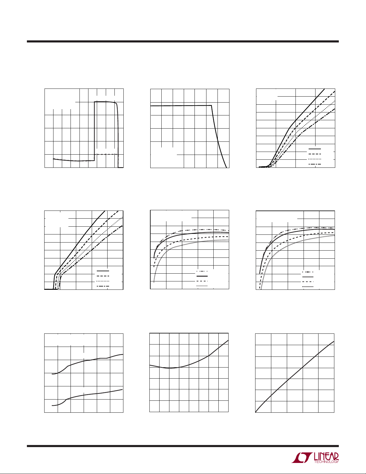
LTC4090 High Voltage Regulator
Effi ciency vs Output Load
100
FIGURE 12 SCHEMATIC
= 4.21V (I
V
95
BAT
90
85
80
75
70
EFFICIENCY (%)
65
60
55
50
0
0.2
BAT
0.4
= 0)
I
OUT
0.6
(A)
HVIN = 8V
HVIN = 12V
HVIN = 24V
HVIN = 36V
0.8
4090 G05
4090 G08
1.0
Ideal Diode Current vs Forward
Voltage and Temperature (No
External Device)
1000
V
= 3.7V
BAT
900
= 0V
V
IN
800
700
600
(mA)
500
OUT
I
400
300
200
100
0
0
50
100
V
(mV)
FWD
LTC4090-5 High Voltage Regulator
Effi ciency vs Output Load
100
FIGURE 12 SCHEMATIC
= 4.21V (I
V
95
BAT
90
85
80
75
70
EFFICIENCY (%)
65
60
55
50
0
0.2
BAT
0.4
= 0)
I
OUT
0.6
(A)
–50°C
50°C
100°C
150
HVIN = 8V
HVIN = 12V
HVIN = 24V
HVIN = 36V
0.8
0°C
200
4090 G06
1.0
4090 G29
High Voltage Regulator Maximum
Load Current
3.0
FIGURE 12 SCHEMATIC
(A)
OUT
I
2.8
2.6
2.4
2.2
2.0
1.8
V
5
= 4.21V (I
BAT
10
= 0)
BAT
TYPICAL
MINIMUM
15 20 25
HVIN (V)
6
30 35
4090 G09
High Voltage Regulator Minimum
Switch On-Time vs Temperature
140
120
100
80
60
40
MINIMUM SWITCH ON TIME (ns)
20
0
–50 25–25 0 50 75 100 150125
TEMPERATURE (˚C)
4090 G10
High Voltage Regulator Switch
Voltage Drop
700
600
500
400
300
VOLTAGE DROP (mV)
200
100
0
0
500 1000 2000 2500
SWITCH CURRENT (mA)
1500
4090 G11
4090fa
TYPICAL PERFORMANCE CHARACTERISTICS
LTC4090/LTC4090-5
High Voltage Regulator Switch
Frequency
1100
1000
900
800
700
FREQUENCY (kHz)
600
500
–50
050
–25 25
TEMPERATURE (°C)
High Voltage Regulator Switch
Current Limit
4.0
3.5
3.0
2.5
2.0
SWITCH CURRENT LIMIT(A)
1.5
1.0
20 60
0
40
DUTY CYCLE (%)
75
100
125
80 100
4090 G12
4090 G15
150
High Voltage Regulator
Frequency Foldback High Voltage Regulator Soft-Start
1000
900
800
700
600
500
400
300
200
SWITCHING FREQUENCY (kHz)
100
0
0
1
2
HVOUT (V)
High Voltage Regulator Switch
Current Limit
4.5
4.0
3.5
3.0
2.5
2.0
1.5
1.0
SWITCH CURRENT LIMIT (A)
0.5
0
–50 25–25 0 50 75 100 150125
DUTY CYCLE = 10 %
DUTY CYCLE = 90 %
TEMPERATURE (°C)
4
3
4090 G13
4090 G16
4.0
3.5
3.0
2.5
2.0
1.5
1.0
SWITCH CURRENT LIMIT (A)
0.5
0
0.5 1 2
0
RUN/SS PIN VOLTAGE (V)
1.5
2.5 3 3.5
High Voltage Regulator Minimum
Input Voltage
7.0
6.5
6.0
5.5
5.0
HVIN (V)
4.5
4.0
3.5
3.0
TO START
TO RUN
1
10 100 1000
LOAD CURRENT (mA)
4090 G14
4090 G17
High Voltage Regulator Boost
Diode VF vs I
1.4
1.2
1.0
(V)
f
0.8
0.6
BOOST DIODE V
0.4
0.2
0
0
F
0.5 1.0 1.5
BOOST DIODE CURRENT (A)
4090 G18
2.0
High Voltage Regulator VC
Voltages
2.50
2.00
1.50
VOLTAGE (V)
1.00
C
V
0.50
CURRENT LIMIT CLAMP
SWITCHING THRESHOLD
0
–50 25–25 0 50 75 100 150125
TEMPERATURE (°C)
4090 G19
High Voltage Regulator Power
Good Threshold
2.90
2.85
2.80
2.75
2.70
HVOUT THRESHOLD VOLTAGE (V)
2.65
–50
–25 0
50
25 75 150
TEMPERATURE (°C)
100 125
4090 G20
4090fa
7
LTC4090/LTC4090-5
TYPICAL PERFORMANCE CHARACTERISTICS
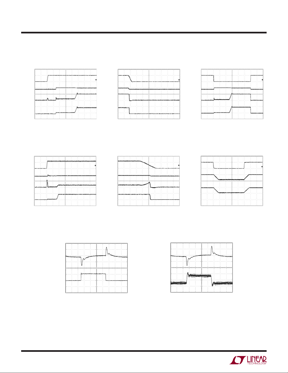
LTC4090 Input Connect
Waveforms
V
IN
5V/DIV
V
OUT
5V/DIV
I
IN
0.5A/DIV
I
BAT
0.5A/DIV
V
= 3.85V
BAT
= 100mA
I
OUT
LTC4090 High Voltage Input
Connect Waveforms
V
HVIN
10V/DIV
V
OUT
5V/DIV
I
HVIN
1A/DIV
I
BAT
1A/DIV
1ms/DIV
4090 G21
LTC4090 Input Disconnect
Waveforms
V
IN
5V/DIV
V
OUT
5V/DIV
I
IN
0.5A/DIV
I
BAT
0.5A/DIV
V
= 3.85V
BAT
= 100mA
I
OUT
LTC4090 High Voltage Input
Disconnect Waveforms
V
HVIN
5V/DIV
V
OUT
5V/DIV
I
HVIN
1A/DIV
I
BAT
1A/DIV
1ms/DIV
4090 G22
LTC4090 Response to Suspend
SUSP
5V/DIV
V
OUT
5V/DIV
I
IN
0.5A/DIV
I
BAT
0.5A/DIV
V
I
BAT
OUT
= 3.85V
= 50mA
1ms/DIV
LTC4090 Response to HPWR
HPWR
5V/DIV
I
IN
0.5A/DIV
I
BAT
0.5A/DIV
4090 G23
V
I
OUT
BAT
= 3.85V
= 100mA
2ms/DIV
4090 G24
LTC4090 High Voltage Regulator
Load Transient
HVOUT
50mV/DIV
I
OUT
1A/DIV
I
LOAD
= 500mA
25μs/DIV
V
I
OUT
BAT
4090 G27
= 3.85V
= 100mA
2ms/DIV
HVOUT
50mV/DIV
1A/DIV
4090 G25
V
I
BAT
OUT
= 3.85V
= 50mA
LTC4090 High Voltage Regulator
Load Transient
I
L
I
LOAD
= 500mA
25μs/DIV
100μs/DIV
4090 G28
4090 G26
8
4090fa

PIN FUNCTIONS
LTC4090/LTC4090-5
SYNC (Pin 1): External Clock Synchronization Input. See
synchronizing section in the Applications Information
section. Ground pin when not used.
PG (Pin 2): The PG pin is the open collector output of an
internal comparator. PG remains low until the HVOUT pin
is above 2.8V. PG output is valid when HVIN is above 3.6V
and HVEN is high.
(Pin 3): Oscillator Resistor Input. Connecting a resistor
R
T
to ground from this pin sets the switching frequency.
(Pin 4): High Voltage Buck Regulator Control Pin. The
V
C
voltage on this pin controls the peak switch current in the
high voltage regulator. Tie an RC network from this pin to
ground to compensate the control loop.
NTC (Pin 5): Input to the NTC Thermistor Monitoring
Circuits. The NTC pin connects to a negative temperature
coeffi cient thermistor which is typically co-packaged with
the battery pack to determine if the battery is too hot or too
cold to charge. If the battery temperature is out of range,
charging is paused until the battery temperature re-enters
the valid range. A low drift bias resistor is required from
VNTC to NTC and a thermistor is required from NTC to
ground. If the NTC function is not desired, the NTC pin
should be grounded.
VNTC (Pin 6): Output Bias Voltage for NTC. A resistor from
this pin to the NTC pin will bias the NTC thermistor.
⎯H⎯V⎯P⎯
R (Pin 7): High Voltage Present Output (Active Low).
A low on this pin indicates that the high voltage regulator
has suffi cient voltage to charge the battery. This feature
is enabled if power is present on HVIN, IN, or BAT (i.e.,
above UVLO thresholds).
⎯C⎯H⎯R⎯
G (Pin 8): Open-Drain Charge Status Output. When the
⎯C⎯H⎯R⎯
battery is being charged, the
internal N-channel MOSFET. When the timer runs out or
the charge current drops below 10% of the programmed
charge current or the input supply is removed, the
pin is forced to a high impedance state.
G pin is pulled low by an
⎯C⎯H⎯R⎯
G
PROG (Pin 9): Charge Current Program Pin. Connecting
a resistor from PROG to ground programs the charge
current:
(),=
50 000
IA
CHG
GATE (Pin 10): External Ideal Diode Gate Connection. This
pin controls the gate of an optional external P-channel
MOSFET transistor used to supplement the internal ideal
diode. The source of the P-channel MOSFET should be
connected to OUT and the drain should be connected to
BAT. When not in use, this pin should be left fl oating. It
is important to maintain high impedance on this pin and
minimize all leakage paths.
BAT (Pin 11): Single-Cell Li-Ion Battery. This pin is used
as an output when charging the battery and as an input
when supplying power to OUT. When the OUT pin potential
drops below the BAT pin potential, an ideal diode function
connects BAT to OUT and prevents OUT from dropping
more than 100mV below BAT. A precision internal resistor
divider sets the fi nal fl oat (charging) potential on this pin.
The internal resistor divider is disconnected when IN and
HVIN are in undervoltage lockout.
IN (Pin 12): Input Supply. Connect to USB supply, V
Input current to this pin is limited to either 20% or 100%
of the current programmed by the CLPROG pin as determined by the state of the HPWR pin. Charge current (to the
BAT pin) supplied through the input is set to the current
programmed by the PROG pin but will be limited by the
input current limit if charge current is set greater than the
input current limit or if the sum of charge current plus load
current is greater than the input current limit.
OUT (Pin 13): Voltage Output. This pin is used to provide
controlled power to a USB device from either USB V
(IN), an external high voltage supply (HVIN), or the battery
(BAT) when no other supply is present. The high voltage
supply is prioritized over the USB V
be bypassed with at least 4.7μF to GND.
R
PROG
V
.
BUS
BUS
input. OUT should
BUS
4090fa
9

LTC4090/LTC4090-5
PIN FUNCTIONS
CLPROG (Pin 14): Current Limit Program and Input Current Monitor. Connecting a resistor, R
CLPROG
, to ground
programs the input to output current limit. The current
limit is programmed as follows:
V
IA
()=
CL
In USB applications, the resistor R
1000
R
CLPROG
CLPROG
should be set
to no less than 2.1k. The voltage on the CLPROG pin is
always proportional to the current fl owing through the
IN to OUT power path. This current can be calculated as
follows:
V
IA
() •= 1000
IN
CLPROG
R
CLPROG
HPWR (Pin 15): High Power Select. This logic input is used
to control the input current limit. A voltage greater than
1.2V on the pin will set the input current limit to 100% of
the current programmed by the CLPROG pin. A voltage
less than 0.4V on the pin will set the input current limit to
20% of the current programmed by the CLPROG pin. A
2μA pull-down current is internally connected to this pin
to ensure it is low at power up when the pin is not being
driven externally.
SUSP (Pin 16): Suspend Mode Input. Pulling this pin
above 1.2V will disable the power path from IN to OUT.
The supply current from IN will be reduced to comply
with the USB specifi cation for suspend mode. Both the
ability to charge the battery from HVIN and the ideal diode
function (from BAT to OUT) will remain active. Suspend
mode will reset the charge timer if OUT is less than BAT
while in suspend mode. If OUT is kept greater than BAT,
such as when the high voltage input is present, the charge
timer will not be reset when the part is put in suspend. A
2μA pull-down current is internally connected to this pin
to ensure it is low at power up when the pin is not being
driven externally.
Charge time is increased if charge current is reduced
due to load current, thermal regulation and current limit
selection (HPWR low).
Shorting the TIMER pin to GND disables the battery
charging functions.
HVOUT (Pin 18): Voltage Output of the High Voltage
Regulator. When suffi cient voltage is present at HVOUT,
the low voltage power path from IN to OUT will be discon-
⎯H⎯V⎯P⎯
nected and the
R pin will be pulled low to indicate
that a high voltage wall adapter has been detected. The
LTC4090 high voltage regulator will maintain just enough
differential voltage between HVOUT and BAT to keep the
battery charger MOSFET out of dropout (typically 300mV
from OUT to BAT). The LTC4090-5 high voltage regulator
will provide a 5V output to the battery charger MOSFET.
HVOUT should be bypassed with at least 22μF to GND.
BOOST (Pin 19): This pin is used to provide drive voltage,
higher than the input voltage, to the internal bipolar NPN
power switch.
SW (Pin 20): The SW pin is the output of the internal high
voltage power switch. Connect this pin to the inductor,
catch diode and boost capacitor.
HVIN (Pin 21): High Voltage Regulator Input. The HVIN pin
supplies current to the internal high voltage regulation and
to the internal high voltage power switch. The presence
of a high voltage input takes priority over the USB V
BUS
input (i.e., when a high voltage input supply is detected,
the USB IN to OUT path is disconnected). This pin must
be locally bypassed.
HVEN (Pin 22): High Voltage Regulator Enable Input. The
HVEN pin is used to disable the high voltage input path.
Tie to ground to disable the high voltage input or tie to at
least 2.3V to enable the high voltage path. If this feature
is not used, tie HVEN to the HVIN pin. This pin can also
be used to soft-start the high voltage regulator; see the
Applications Information section for more information.
TIMER (Pin 17): Timer Capacitor. Placing a capacitor,
C
, to GND sets the timer period. The timer period
TIMER
is:
t hours
TIMER
()
=
C R hours
••
TIMER PROG
µF k
.•
0 1 100
3
10
Exposed Pad (Pin 23): Ground. The exposed package pad
is ground and must be soldered to the PC board for proper
functionality and for maximum heat transfer (use several
vias directly under the LTC4090/LTC4090-5).
4090fa

BLOCK DIAGRAM
HVIN
10
INTERNAL
REFERENCE
HVEN
10
R
T
10
R
T1
R
C
C
C
R
CLPROG
SYNC
10
V
C
10
C
F
PG
10
IN
10
I
IN
1000
CLPROG
22
HPWR
13
1V
500mA/100mA
SOFT-START
VC CLAMP
+
CL
–
2μA
CURRENT
CONTROL
+
I
L
–
OSCILLATOR
200kHz - 2.4MHz
DIE
TEMP
–
TA
I
LIM
105°C
+
+
–
2.8V
SOFT-START
+
–
–
GM
+
+
CURRENT LIMIT
IN
IN OUT BAT
I
LIM
ENABLE
CNTL
RSQ
Q
V
SET
3.6V (LTC4090)
5V (LTC4090-5)
350mV
+
–
(LTC4090)
LTC4090/LTC4090-5
75mV (RISING)
+
25mV (FALLING)
–
4.25V (RISING)
3.15V (FALLING)
CC/CV REGULATOR
CHARGER
ENABLE
DRIVER
BOOST
–
+
+
–
30mV
IDEAL
DIODE
C2
Q1
–
+
20mV
–
+
SW
HVOUT
HVPR
OUTOUT
–
GATE
EDA
+
BATBAT
L1
D1
C1
19
21
21
21
R
10k
PROG
10k
STOP
+
–
+
–
+
–
0.25V
2.9V
BATTERY
UVLO
4.1V
RECHARGE
TIMER
CHRG
21
C
TIMER
18
I
CHG
SOFT-START2
CHG
CHARGE CONTROL
1V
+
–
PROG
23
VOLTAGE DETECT
V
NTC
15
–
NTC
14
T
+
–
TOO
COLD
TOO
HOT
NTCERR
UVLO
CONTROL LOGIC
BAT UV
RECHRG
HOLD
RESET
OSCILLATOR
CLK
COUNTER
+
EOC
C/10
4090 BD
0.1V
+
NTC ENABLE
2μA
–
GND SUSP
16
11
4090fa
11

LTC4090/LTC4090-5
OPERATION
Introduction
TM
The LTC4090/LTC4090-5 are complete PowerPath
controllers for battery powered USB applications. The
LTC4090/LTC4090-5 are designed to receive power from
a low voltage source (e.g., USB or 5V wall adapter), a
high voltage source (e.g., FireWire/IEEE1394, automotive
battery, 12V wall adapter, etc.), and a single-cell Li-Ion
battery. They can then deliver power to an application
connected to the OUT pin and a battery connected to the
BAT pin (assuming that an external supply other than
the battery is present). Power supplies that have limited
current resources (such as USB V
supplies) should
BUS
be connected to the IN pin which has a programmable
current limit. Battery charge current will be adjusted to
ensure that the sum of the charge current and load current does not exceed the programmed input current limit
(see Figure 1).
An ideal diode function provides power from the battery
when output / load current exceeds the input current limit or
when input power is removed. Powering the load through
the ideal diode instead of connecting the load directly to
the battery allows a fully charged battery to remain fully
charged until external power is removed. Once external
power is removed the output drops until the ideal diode is
forward biased. The forward biased ideal diode will then
provide the output power to the load from the battery.
The LTC4090/LTC4090-5 also include a high voltage
switching regulator which has the ability to receive power
from a high voltage input. This input takes priority over the
USB V
input (i.e., if both HVIN and IN are present, load
BUS
current and charge current will be delivered via the high
voltage path). When enabled, the high voltage regulator
regulates the HVOUT voltage using a constant frequency,
current mode regulator. An external PFET between HVOUT
⎯H⎯V⎯P⎯
(drain) and OUT (source) is turned on via the
R pin
allowing OUT to charge the battery and/or supply power
to the application. The LTC4090’s Bat-Track maintains
approximately 300mV between the OUT pin and the BAT
pin, while the LTC4090-5 provides a fi xed 5V output.
PowerPath is a trademark of Linear Technology Corporation
HVIN
IN
BUCK REGULATOR
ENABLE
USB CURRENT LIMIT
HIGH VOLTAGE
3.15V (FALLING)
+
–
4.25V (RISING)
75mV (RISING)
25mV (FALLING)
CC/CV REGULATOR
CHARGER
SW
HVOUT
HVPR
OUT
GATE
BATBAT
L1
D1
C1
LOAD
+
Li-Ion
Q1
+
–
EDA
19
21
21
21
4090 F01
OUT
+
–
–
+
30mV
+
–
30mV
IDEAL
DIODE
–
+
12
Figure 1. Simplifi ed PowerPath Block Diagram
4090fa

OPERATION
LTC4090/LTC4090-5
USB Input Current Limit
The input current limit and charge control circuits of the
LTC4090/LTC4090-5 are designed to limit input current as
well as control battery charge current as a function of I
OUT
.
OUT drives the external load and the battery charger.
If the combined load at OUT does not exceed the programmed input current limit, OUT will be connected to IN
through an internal 215mΩ P-channel MOSFET.
If the combined load at OUT exceeds the programmed input
current limit, the battery charger will reduce its charge current by the amount necessary to enable the external load
to be satisfi ed while maintaining the programmed input
current. Even if the battery charge current is set to exceed
the allowable USB current, a correctly programmed input
current limit will ensure that the USB specifi cation is never
violated. Furthermore, load current at OUT will always be
prioritized and only excess available current will be used
to charge the battery.
The input current limit, I
, can be programmed using the
CL
following formula:
I
=
CL
where V
and R
CLPROG
⎛
1000 1000
⎜
R
⎝
CLPROG
CLPROG
V
•
CLPROG
is the CLPROG pin voltage (typically 1V)
is the total resistance from the CLPROG pin
⎞
⎟
⎠
=
R
CLPROG
V
to ground. For best stability over temperature and time,
1% metal fi lm resistors are recommended.
The programmed battery charge current, I
, is defi ned
CHG
as:
and quiescent currents. A 2.1k CLPROG resistor will give a
typical current limit of 476mA in high power mode (when
HPWR is high) or 95mA in low power mode (when HPWR
is low).
When SUSP is driven to a logic high, the input power
path is disabled and the ideal diode from BAT to OUT will
supply power to the application.
High Voltage Step Down Regulator
The power delivered from HVIN to HVOUT is controlled by
a constant frequency, current mode step down regulator.
An external P-channel MOSFET directs this power to OUT
and prevents reverse conduction from OUT to HVOUT (and
ultimately HVIN).
An oscillator, with frequency set by R
, enables an RS fl ip-
T
fl op, turning on the internal power switch. An amplifi er and
comparator monitor the current fl owing between HVIN and
SW pins, turning the switch off when this current reaches
a level determined by the voltage at V
servos the V
node to maintain approximately 300mV
C
. An error amplifi er
C
between OUT and BAT (LTC4090). By keeping the voltage
across the battery charger low, effi ciency is optimized because power lost to the battery charger is minimized and
power available to the external load is maximized. If the
BAT pin voltage is less than approximately 3.3V, then the
error amplifi er will servo the V
node to provide a constant
C
HVOUT output voltage of about 3.6V (LTC4090). An active
clamp on the V
node provides current limit. The VC node
C
is also clamped to the voltage on the HVEN pin; soft-start
is implemented by generating a voltage ramp at the HVEN
pin using an external resistor and capacitor.
⎛
I
CHG
50 000 50 000,
=
⎜
R
⎝
•
PROG
V
PROG
⎞
=
⎟
⎠
,
R
PROG
V
Input current, IIN, is equal to the sum of the BAT pin output
current and the OUT pin output current. V
CLPROG
will track
the input current according to the following equation:
V
II I
=+= • 1000
IN OUT BAT
In USB applications, the maximum value for R
CLPROG
R
CLPROG
CLPROG
should be 2.1k. This will prevent the input current from
exceeding 500mA due to LTC4090/LTC4090-5 tolerances
The switch driver operates from either the high voltage
input or from the BOOST pin. An external capacitor and
internal diode are used to generate a voltage at the BOOST
pin that is higher than the input supply. This allows the
driver to fully saturate the internal bipolar NPN power
switch for effi cient operation.
To further optimize effi ciency, the high voltage buck regu-
®
lator automatically switches to Burst Mode
operation in
light load situations. Between bursts, all circuitry associated
with controlling the output switch is shut down reducing
the input supply current.
4090fa
13

LTC4090/LTC4090-5
OPERATION
I
I
LOAD
IN
500
400
300
100
I
IN
80
I
60
LOAD
500
400
300
I
BAT
= I
CHG
I
IN
I
LOAD
200
CURRENT (mA)
100
4090 F02a
0
100 200
0
(CHARGING)
I
LOAD(mA)
I
BAT
400 500300
(IDEAL DIODE)
(a) High Power Mode/Full Charge
R
= 100k and R
PROG
CLPROG
= 2k
I
BAT
40
CURRENT (mA)
20
0
20 40
0
4090 F02b
(a) Low Power Mode/Full Charge
R
= 100k and R
PROG
Figure 2. Input and Battery Currents as a Function of Load Current
The oscillator reduces the switch regulator’s operating
frequency when the voltage at the HVOUT pin is low (below 2.95V). This frequency foldback helps to control the
output current during start-up and overload.
The high voltage regulator contains a power good comparator which trips when the HVOUT pin is at 2.8V. The PG
output is an open-collector transistor that is off when the
output is in regulation, allowing an external resistor to pull
the PG pin high. Power good is valid when the switching
regulator is enabled and HVIN is above 3.6V.
Ideal Diode From BAT to OUT
The LTC4090/LTC4090-5 have an internal ideal diode as
well as a controller for an optional external ideal diode. If
a battery is the only power supply available, or if the load
current exceeds the programmed input current limit, then
the battery will automatically deliver power to the load via
an ideal diode circuit between the BAT and OUT pins. The
ideal diode circuit (along with the recommended 4.7μF
capacitor on the OUT pin) allows the LTC4090/LTC4090-5
to handle large transient loads and wall adapter or USB
connect/disconnect scenarios without the need for
V
BUS
large bulk capacitors. The ideal diode responds within
a few microseconds and prevents the OUT pin voltage
from dropping signifi cantly below the BAT pin voltage.
A comparison of the I-V curve of the ideal diode and a
Schottky diode can be seen in Figure 3.
200
(CHARGING)
I
LOAD(mA)
I
BAT
80 10060
(IDEAL DIODE)
CURRENT (mA)
100
0
100 200
I
BAT
0
4090 F02c
(CHARGING)
I
LOAD (mA)
I
= I
BAT
I
BAT
400 500300
(IDEAL DIODE)
= I
CL
OUT
I
BAT
(a) High Power Mode with
CLPROG
= 2k
ICL = 500mA and I
R
= 100k and R
PROG
= 250mA
CHG
CLPROG
= 2k
If the desired input current increases beyond the programmed input current limit additional current will be drawn
from the battery via the internal ideal diode. Furthermore,
if power to IN (USB V
) or HVIN (high voltage input) is
BUS
removed, then all of the application power will be provided
by the battery via the ideal diode. A 4.7μF capacitor at
OUT is suffi cient to keep a transition from input power
to battery power from causing signifi cant output voltage
droop. The ideal diode consists of a precision amplifi er that
enables a large P-channel MOSFET transistor whenever the
voltage at OUT is approximately 20mV (V
) below the
FWD
voltage at BAT. The resistance of the internal ideal diode
is approximately 215mΩ.
If this is suffi cient for the application then no external
components are necessary. However if more conductance
is needed, an external P-channel MOSFET can be added
from BAT to OUT. The GATE pin of the LTC4090/LTC4090-5
drives the gate of the external PFET for automatic ideal
diode control. The source of the external MOSFET should
be connected to OUT and the drain should be connected
to BAT. In order to help protect the external MOSFET in
overcurrent situations, it should be placed in close thermal
contact to the LTC4090/LTC4090-5.
Burst Mode is a registered trademark of Linear Technology Corporation
4090fa
14

OPERATION
LTC4090/LTC4090-5
Suspend Mode
When SUSP is pulled above V
the LTC4090/LTC4090-5
IH
enter suspend mode to comply with the USB specifi cation.
In this mode, the power path between IN and OUT is put
in a high impedance state to reduce the IN input current to
50μA. If no other power source is available to drive HVIN,
the system load connected to OUT is supplied through the
ideal diodes connected to BAT.
Battery Charger
The battery charger circuits of the LTC4090/LTC4090-5
are designed for charging single cell lithium-ion batteries.
Featuring an internal P-channel power MOSFET, the charger
uses a constant current / constant voltage charge algorithm
with programmable charge current and a programmable
timer for charge termination. Charge current can be
programmed up to 1.5A. The fi nal fl oat voltage accuracy
is ±0.8% typical. No blocking diode or sense resistor is
required when powering either the IN or the HVIN pins.
⎯C⎯H⎯R⎯
The
G open-drain status output provides information
regarding the charging status of the LTC4090/LTC4090-5
at all times. An NTC input provides the option of charge
qualifi cation using battery temperature.
trickle charge mode to bring the cell voltage up to a safe
level for charging. The charger goes into the fast charge
constant current mode once the voltage on the BAT pin
rises above 2.9V. In constant current mode, the charge
current is set by R
. When the battery approaches the
PROG
fi nal fl oat voltage, the charge current begins to decrease
as the LTC4090/LTC4090-5 switch to constant voltage
mode. When the charge current drops below 10% of the
programmed value while in constant voltage mode the
⎯C⎯H⎯R⎯
G pin assumes a high impedance state.
An external capacitor on the TIMER pin sets the total
minimum charge time. When this time elapses, the
⎯C⎯H⎯R⎯
charge cycle terminates and the
G pin assumes a
high impedance state, if it has not already done so. While
charging in constant current mode, if the charge current
is decreased by thermal regulation or in order to maintain
the programmed input current limit, the charge time is
automatically increased. In other words, the charge time is
extended inversely proportional to the actual charge current
delivered to the battery. For Li-Ion and similar batteries that
require accurate fi nal fl oat potential, the internal bandgap
reference, voltage amplifi er and the resistor divider provide
regulation with ±0.8% accuracy.
The charge cycle begins when the voltage at the OUT
pin rises above the battery voltage and the battery voltage is below the recharge threshold. No charge current
actually fl ows until the OUT voltage is 100mV above
the BAT voltage. At the beginning of the charge cycle, if
the battery voltage is below 2.9V, the charger goes into
LTC4090/LTC4090-5
I
MAX
SLOPE: 1/R
I
FWD
CURRENT (A)
SLOPE: 1/R
0
Figure 3. LTC4090/LTC4090-5 Versus Schottky Diode Forward
Voltage Drop
FORWARD VOLTAGE (V)
V
FWD
FWD
DIO(ON)
SCHOTTKY
DIODE
CONSTANT
I
0N
CONSTANT
R
0N
CONSTANT
V
0N
4090 F03
Trickle Charge and Defective Battery Detection
At the beginning of a charge cycle, if the battery voltage
is below 2.9V, the charger goes into trickle charge reducing the charge current to 10% of the full-scale current.
If the low battery voltage persists for one quarter of the
programmed total charge time, the battery is assumed
to be defective, the charge cycle is terminated and the
⎯C⎯H⎯R⎯
G pin output assumes a high impedance state. If
for any reason the battery voltage rises above ~2.9V the
charge cycle will be restarted. To restart the charge cycle
(i.e., when the dead battery is replaced with a discharged
battery), simply remove the input voltage and reapply it
or cycle the TIMER pin to 0V.
Programming Charge Current
The formula for the battery charge current is:
V
II
==•, •,50 000 50 000
CHG PROG
PROG
R
PROG
4090fa
15

LTC4090/LTC4090-5
OPERATION
where V
is the PROG pin voltage and R
PROG
PROG
is the
total resistance from the PROG pin to ground. Keep in
mind that when the LTC4090/LTC4090-5 are powered
from the IN pin, the programmed input current limit takes
precedence over the charge current. In such a scenario,
the charge current cannot exceed the programmed input
current limit.
For example, if typical 500mA charge current is required,
calculate:
V
R
PROG
1
==
500
50 000 100•,
mA
k
For best stability over temperature and time, 1% metal
fi lm resistors are recommended. Under trickle charge
conditions, this current is reduced to 10% of the fullscale value.
The Charge Timer
The programmable charge timer is used to terminate the
charge cycle. The timer duration is programmed by an
external capacitor at the TIMER pin. The charge time is
typically:
t hours
TIMER
()
=
C R hours
••
TIMER PROG
µF k
.•
0 1 100
3
The timer starts when an input voltage greater than the
undervoltage lockout threshold level is applied or when
leaving shutdown and the voltage on the battery is less than
the recharge threshold. At power-up or exiting shutdown
with the battery voltage less than the recharge threshold,
the charge time is a full cycle. If the battery is greater than
the recharge threshold the timer will not start and charging
is prevented. If after power-up the battery voltage drops
below the recharge threshold, or if after a charge cycle
the battery voltage is still below the recharge threshold,
the charge time is set to one-half of a full cycle.
The LTC4090/LTC4090-5 have a feature that extends charge
time automatically. Charge time is extended if the charge
current in constant current mode is reduced due to load
current or thermal regulation. This change in charge time
is inversely proportional to the change in charge current.
As the LTC4090/LTC4090-5 approach constant voltage
mode the charge current begins to drop. This change in
charge current is due to normal charging operation and
does not affect the timer duration.
Consider, for example, a USB charge condition where
R
CLPROG
= 2k, R
= 100k and C
PROG
= 0.1μF. This
TIMER
corresponds to a three hour charge cycle. However, if the
HPWR input is set to a logic low, then the input current
limit will be reduced from 500mA to 100mA. With no additional system load, this means the charge current will
be reduced to 100mA. Therefore, the termination timer
will automatically slow down by a factor of fi ve until the
charger reaches constant voltage mode (i.e. V
BAT
approaches 4.2V) or HPWR is returned to a logic high. The
charge cycle is automatically lengthened to account for
the reduced charge current. The exact time of the charge
cycle will depend on how long the charger remains in
constant current mode and/or how long the HPWR pin
remains logic low.
Once a time-out occurs and the voltage on the battery is
greater than the recharge threshold, the charge current
⎯C⎯H⎯R⎯
stops, and the
G output assumes a high impedance
state if it has not already done so.
Connecting the TIMER pin to ground disables the battery
charger.
⎯C⎯H⎯R⎯
G Status Output Pin
⎯C⎯H⎯R⎯
When the charge cycle starts, the
G pin is pulled to
ground by an internal N-channel MOSFET capable of driving an LED. When the charge current drops below 10%
of the programmed full charge current while in constant
voltage mode, the pin assumes a high impedance state,
but charge current continues to fl ow until the charge
time elapses. If this state is not reached before the end
of the programmable charge time, the pin will assume a
⎯C⎯H⎯R⎯
high impedance state when a time-out occurs. The
G
current detection threshold can be calculated by the following equation:
I
DETECT
V
01
==
R
PROG PROG
50 000
•,
V
5000.
R
16
4090fa

OPERATION
LTC4090/LTC4090-5
For example, if the full charge current is programmed
⎯C⎯H⎯R⎯
to 500mA with a 100k PROG resistor the
G pin will
change state at a battery charge current of 50mA.
Note: The end-of-charge (EOC) comparator that monitors the charge current latches its decision. Therefore,
the fi rst time the charge current drops below 10% of the
programmed full charge current while in constant volt-
⎯C⎯H⎯R⎯
age mode, it will toggle
G to a high impedance state.
If, for some reason the charge current rises back above
⎯C⎯H⎯R⎯
the threshold, the
G pin will not resume the strong
pull-down state. The EOC latch can be reset by a recharge
cycle (i.e., V
drops below the recharge threshold) or
BAT
toggling the input power to the part.
Automatic Recharge
After the battery charger terminates, it will remain off
drawing only microamperes of current from the battery. If
the product remains in this state long enough, the battery
will eventually self discharge. To ensure that the battery is
always topped off, a charge cycle will automatically begin
when the battery voltage falls below V
RECHRG
4.1V). To prevent brief excursions below V
(typically
RECHRG
from
resetting the safety timer, the battery voltage must be
below V
RECHRG
for more than a few milliseconds. The
charge cycle and safety timer will also restart if the IN
UVLO cycles low and then high (e.g. IN, is removed and
then replaced).
Thermal Regulation
To prevent thermal damage to the IC or surrounding
components, an internal thermal feedback loop will
automatically decrease the programmed charge current
if the die temperature rises to approximately 105°C.
Thermal regulation protects the LTC4090/LTC4090-5
from excessive temperature due to high power operation
or high ambient thermal conditions and allows the user
to push the limits of the power handling capability with a
given circuit board design without risk of damaging the
LTC4090/LTC4090-5 or external components. The benefi t
of the LTC4090/LTC4090-5 thermal regulation loop is that
charge current can be set according to actual conditions
rather than worst-case conditions with the assurance that
the battery charger will automatically reduce the current
in worst-case conditions.
Undervoltage Lockout
An internal undervoltage lockout circuit monitors the input
voltage (IN) and the output voltage (OUT) and disables
either the input current limit or the battery charger circuits
or both. The input current limit circuitry is disabled until
rises above the undervoltage lockout threshold and VIN
V
IN
exceeds V
abled until V
by 50mV. The battery charger circuits are dis-
OUT
exceeds V
OUT
by 50mV. Both undervoltage
BAT
lockout comparators have built-in hysteresis.
NTC Thermistor
The battery temperature is measured by placing a negative temperature coeffi cient (NTC) thermistor close to
the battery pack. To use this feature connect the NTC
thermistor, R
bias resistor, R
, between the NTC pin and ground and a
NTC
, from VNTC to NTC. R
NOM
should be
NOM
a 1% resistor with a value equal to the value of the chosen
NTC thermistor at 25°C (denoted R
25C
).
The LTC4090/LTC4090-5 will pause charging when the
resistance of the NTC thermistor drops to 0.41 times the
value of R
or approximately 4.1k (for a Vishay “Curve
25C
2” thermistor, this corresponds to approximately 50°C).
The safety timer also pauses until the thermistor indicates
a return to a valid temperature. As the temperature drops,
the resistance of the NTC thermistor rises. The LTC4090/
LTC4090-5 are also designed to pause charging (and timer)
when the value of the NTC thermistor increases to 2.82
times the value of R
. For a Vishay “Curve 2” thermistor
25C
this resistance, 28.2k, corresponds to approximately 0°C.
The hot and cold comparators each have approximately
3°C of hysteresis to prevent oscillation about the trip point.
Grounding the NTC pin disables all NTC functionality.
4090fa
17

LTC4090/LTC4090-5
APPLICATIONS INFORMATION
USB and 5V Wall Adapter Power
Although the LTC4090/LTC4090-5 are designed to draw
power from a USB port, a higher power 5V wall adapter
can also be used to power the application and charge the
battery (higher voltage wall adapters can be connected
directly to HVIN). Figure 4 shows an example of combining
a 5V wall adapter and a USB power input. With its gate
grounded by 1k, P-channel MOSFET MP1 provides USB
power to the LTC4090/LTC4090-5 when 5V wall power is
not available. When 5V wall power is available, diode D1
supplies power to the LTC4090/LTC4090-5, pulls the gate
of MN1 high to increase the charge current (by increasing
the input current limit), and pulls the gate of MP1 high to
disable it and prevent conduction back to the USB port.
Setting the Switching Frequency
The high voltage switching regulator uses a constant
frequency PWM architecture that can be programmed to
switch from 200kHz to 2.4MHz by using a resistor tied
from the R
value for a desired switching frequency is in Table 1.
R
T
Table 1. Switching Frequency vs RT Value
SWITCHING FREQUENCY (MHz) RT VALUE (kΩ)
pin to ground. A table showing the necessary
T
0.2 187
0.3 121
0.4 88.7
0.5 68.1
0.6 56.2
0.7 46.4
0.8 40.2
0.9 34.0
1.0 29.4
1.2 23.7
1.4 19.1
1.6 16.2
1.8 13.3
2.0 11.5
2.2 9.76
2.4 8.66
5V WALL
ADAPTER
850mA I
CHG
USB POWER
500mA I
CHG
BAT
D1
MP1
Figure 4. USB or 5V Wall Adapter Power
IN
MN1
LTC4090
PROG
CLPROG
2.87k
I
CHG
+
Li-Ion
BATTERY
2k1k
59k
4090 F04
Operating Frequency Tradeoffs
Selection of the operating frequency for the high voltage
buck regulator is a tradeoff between effi ciency, component
size, minimum dropout voltage, and maximum input voltage. The advantage of high frequency operation is that
smaller inductor and capacitor values may be used. The
disadvantages are lower effi ciency, lower maximum input
voltage, and higher dropout voltage. The highest acceptable
switching frequency (f
SW(MAX)
) for a given application can
be calculated as follows:
VV
+
f
SW MAX
where V
V
HVOUT
=
()
tVVV
ON MIN D HVIN SW
is the typical high voltage input voltage,
HVIN
is the output voltage of the switching regulator, VD
is the catch diode drop (~0.5V), and V
D HVOUT
•–
+
()
()
is the internal
SW
switch drop (~0.5V at max load). This equation shows
that slower switching frequency is necessary to safely
accommodate high V
HVIN/VHVOUT
ratio. Also, as shown in
the next section, lower frequency allows a lower dropout
voltage. The reason input voltage range depends on the
switching frequency is because the high voltage switch
has fi nite minimum on and off times. The switch can turn
on for a minimum of ~150ns and turn off for a minimum
of ~150ns. This means that the minimum and maximum
duty cycles are:
DC
DC
where fSW is the switching frequency, t
minimum switch-on time (~150ns), and t
= fSW • t
MIN
= 1 – fSW • t
MAX
ON(MIN)
OFF(MIN)
ON(MIN)
OFF(MIN)
is the
is the
18
4090fa

APPLICATIONS INFORMATION
LTC4090/LTC4090-5
minimum switch-off time (~150ns). These equations show
that duty cycle range increases when switching frequency
is decreased.
A good choice of switching frequency should allow adequate input voltage range (see next section) and keep
the inductor and capacitor values small.
HVIN Input Voltage Range
The maximum input voltage range for the LTC4090/
LTC4090-5 applications depends on the switching frequency, the Absolute Maximum Ratings of the V
HVIN
and
BOOST pins, and the operating mode.
The high voltage switching regulator can operate from
input voltages up to 36V, and safely withstand input voltages up to 60V. Note that while V
> 41.5V (typical),
HVIN
the LTC4090/LTC4090-5 will stop switching, allowing the
output to fall out of regulation.
While the high voltage regulator output is in start-up,
short-circuit, or other overload conditions, the switching
frequency should be chosen according to the following
discussion.
For safe operation at inputs up to 60V the switching frequency must be low enough to satisfy V
HVIN(MAX)
according to the following equation. If lower V
≥ 45V
HVIN(MAX)
is desired, this equation can be used directly.
V
HVIN MAX
where V
V
HVOUT
HVIN(MAX)
is the high voltage regulator output voltage, VD is
ft
SW ON MIN
is the maximum operating input voltage,
the catch diode drop (~0.5V), V
drop (~0.5V at max load), f
VV
(set by R
), and t
T
ON(MIN)
+
HVOUT D
•
()
VV
–=
+
DSW()
is the internal switch
SW
is the switching frequency
SW
is the minimum switch-on time
(~150ns). Note that a higher switching frequency will depress the maximum operating input voltage. Conversely,
a lower switching frequency will be necessary to achieve
safe operation at high input voltages.
If the output is in regulation and no short-circuit, startup, or overload events are expected, then input voltage
transients of up to 60V are acceptable regardless of the
switching frequency. In this mode, the LTC4090/LTC4090-5
may enter pulse skipping operation where some switching pulses are skipped to maintain output regulation. In
this mode the output voltage ripple and inductor current
ripple will be higher than in normal operation. Above 41.5V,
switching will stop.
The minimum input voltage is determined by either the high
voltage regulator’s minimum operating voltage of ~6V or by
its maximum duty cycle (see equation in previous section).
The minimum input voltage due to duty cycle is:
V
HVIN MIN
where V
t
OFF(MIN)
VV
HVOUT D
=
−
1
HVIN(MIN)
is the minimum input voltage, and
is the minimum switch off time (150ns). Note
+
ft
SW OFF MIN
()
VV
−+
DSW()
that higher switching frequency will increase the minimum
input voltage. If a lower dropout voltage is desired, a lower
switching frequency should be used.
Inductor Selection and Maximum Output Current
A good choice for the inductor value is L = 6.8μH (assuming a 800kHz operating frequency). With this value the
maximum load current will be ~2.4A. The RMS current
rating of the inductor must be greater than the maximum
load current and its saturation current should be about
30% higher. Note that the maximum load current will be
programmed charge current plus the largest expected
application load current. For robust operation in fault
conditions, the saturation current should be ~3.5A. To
keep effi ciency high, the series resistance (DCR) should
be less than 0.1Ω. Table 2 lists several vendors and types
that are suitable.
Table 2. Inductor Vendors
VENDOR URL PART SERIES TYPE
Murata www.murata.com LQH55D Open
TDK www.componenttdk.com SLF7045
SLF10145
Toko www.toko.com D62CB
D63CB
D75C
D75F
Sumida www.sumida.com CR54
CDRH74
CDRH6D38
CR75
Shielded
Shielded
Shielded
Shielded
Shielded
Open
Open
Shielded
Shielded
Open
4090fa
19

LTC4090/LTC4090-5
APPLICATIONS INFORMATION
Catch Diode
The catch diode conducts current only during switch-off
time. Average forward current in normal operation can
be calculated from:
VV
II
D AVG HVOUT
=
()
where I
is the output load current. The only reason to
HVOUT
()
•
–
HVIN HVOUT
V
HVIN
consider a diode with a larger current rating than necessary
for nominal operation is for the worst-case condition of
shorted output. The diode current will then increase to the
typical peak switch current. Peak reverse voltage is equal
to the regulator input voltage. Use a Schottky diode with a
reverse voltage rating greater than the input voltage. The
overvoltage protection feature in the high voltage regulator
will keep the switch off when V
the use of 45V rated Schottky even when V
> 45V which allows
HVIN
HVIN
ranges
up to 60V. Table 3 lists several Schottky diodes and their
manufacturers.
Table 3. Diode Vendors
PART NUMBER
On Semiconductor
MBRM120E
MBRM140
Diodes Inc.
B130
B220
B230
B360
DFLS240L
International Rectifi er
10BQ030
20BQ030
V
(V)
20
40
30
20
30
60
40
30
30
R
I
(A)
AVE
1
1
1
2
2
3
2
1
2
AT 1A
V
F
(MV)
530
550
500
500
420 470
VF AT 2A
(MV)
595
500
500
550
500
470
High Voltage Regulator Output Capacitor Selection
The high voltage regulator output capacitor has two essential functions. Along with the inductor, it fi lters the
square wave generated at the switch pin to produce the
DC output. In this role it determines the output ripple, and
low impedance at the switching frequency is important.
The second function is to store energy in order to satisfy
transient loads and stabilize the LTC4090/LTC4090-5’s
control loop. Ceramic capacitors have very low equivalent series resistance (ESR) and provide the best ripple
performance. A good starting value is:
C
OUT
where fSW is in MHz, and C
100
=
Vf
OUT SW
is the recommended output
OUT
capacitance in μF. Use X5R or X7R types. This choice will
provide low output ripple and good transient response.
Transient performance can be improved with a higher value
capacitor if the compensation network is also adjusted
to maintain the loop bandwidth. A lower value of output
capacitor can be used to save space and cost but transient
performance will suffer. See the High Voltage Regulator
Frequency Compensation section to choose an appropriate
compensation network.
When choosing a capacitor, look carefully through the
data sheet to fi nd out what the actual capacitance is under
operating conditions (applied voltage and temperature).
A physically larger capacitor, or one with a higher voltage
rating, may be required. High performance tantalum or
electrolytic capacitors can be used for the output capacitor.
Low ESR is important, so choose one that is intended for
use in switching regulators. The ESR should be specifi ed
by the supplier, and should be 0.05Ω or less. Such a
capacitor will be larger than a ceramic capacitor and will
have a larger capacitance, because the capacitor must be
large to achieve low ESR.
Ceramic Capacitors
Ceramic capacitors are small, robust and have very low
ESR. However, ceramic capacitors can cause problems
when used with the high voltage switching regulator
due to their piezoelectric nature. When in Burst Mode
operation, the LTC4090/LTC4090-5’s switching frequency
depends on the load current, and at very light loads the
LTC4090/LTC4090-5 can excite the ceramic capacitor at
audio frequencies, generating audible noise. Since the
LTC4090/LTC4090-5 operate at a lower current limit during
Burst Mode operation, the noise is typically very quiet to a
casual ear. If this is unacceptable, use a high performance
tantalum or electrolytic capacitor at the output.
High Voltage Regulator Frequency Compensation
The LTC4090/LTC4090-5 high voltage regulator uses
current mode control to regulate the output. This simplifi es loop compensation. In particular, the high voltage
4090fa
20

APPLICATIONS INFORMATION
5
LTC4090/LTC4090-5
regulator does not require the ESR of the output capacitor
for stability, so you are free to use ceramic capacitors to
achieve low output ripple and small circuit size. Frequency
compensation is provided by the components tied to the
pin, as shown in Figure 1. Generally a capacitor (CC)
V
C
and a resistor (R
) in series to ground are used. In ad-
C
dition, there may be a lower value capacitor in parallel.
This capacitor (C
) is not part of the loop compensation
F
but is used to fi lter noise at the switching frequency, and
is required only if a phase-lead capacitor is used or if the
output capacitor has high ESR.
Loop compensation determines the stability and transient
performance. Designing the compensation network is a bit
complicated and the best values depend on the application
and in particular the type of output capacitor. A practical
approach is to start with the front page schematic and tune
the compensation network to optimize performance. Stability should then be checked across all operating conditions,
including load current, input voltage and temperature. The
LTC1375 datasheet contains a more thorough discussion
of loop compensation and describes how to test the stability using a transient load. Figure 5 shows the transient
response when the load current is stepped from 500mA
to 1500mA and back to 500mA.
Low Ripple Burst Mode Operation and Pulse-Skip
Mode
The LTC4090/LTC4090-5 are capable of operating in either
low ripple Burst Mode operation or pulse-skip mode which
are selected using the SYNC pin. Tie the SYNC pin below
V
or above V
(typically 0.5V) for low ripple Burst Mode operation
SYNC,L
(typically 0.8V) for pulse-skip mode.
SYNC,H
To enhance effi ciency at light loads, the LTC4090/LTC4090-5
can be operated in low ripple Burst Mode operation which
keeps the output capacitor charged to the proper voltage
while minimizing the input quiescent current. During Burst
Mode operation, the LTC4090/LTC4090-5 deliver single
cycle bursts of current to the output capacitor followed
by sleep periods where the output power is delivered to
the load by the output capacitor. Because the LTC4090/
LTC4090-5 deliver power to output with single, low current
pulses, the output ripple is kept below 15mV for a typical
application. As the load current decreases towards a no
load condition, the percentage of time that the high voltage regulator operates in sleep mode increases and the
average input current is greatly reduced resulting in high
effi ciency even at very low loads. See Figure 6.
At higher output loads (above 70mA for the front page
application) the LTC4090/LTC4090-5 will be running at
the frequency programmed by the R
resistor, and will be
T
operating in standard PWM mode. The transition between
PWM and low ripple Burst Mode operation is seamless,
and will not disturb the output voltage.
If low quiescent current is not required, the LTC4090/
LTC4090-5 can operate in pulse-skip mode. The benefi t
of this mode is that the LTC4090/LTC4090-5 will enter full
frequency standard PWM operation at a lower output load
current than when in Burst Mode operation. The front page
application circuit will switch at full frequency at output
loads higher than about 60mA.
VIN = 12V; FIGURE 12 SCHEMATIC
= 10mA
I
LOAD
I
L
0.5A/DIV
FIGURE 12 SCHEMATIC
HVOUT
50mV/DIV
I
L
1A/DIV
25μs/DIV
Figure 5. Transient Load Response of the LTC4090 High Voltage
Regulator Front Page Application as the Load Current is Stepped
from 500mA to 1500mA.
4090 F0
V
SW
5V/DIV
V
OUT
10mV/DIV
5μs/DIV
Figure 6. High Voltage Regulator Burst Mode Operation
4090 F06
4090fa
21

LTC4090/LTC4090-5
APPLICATIONS INFORMATION
Boost Pin Considerations
Capacitor C2 (see Block Diagram) and an internal diode
are used to generate a boost voltage that is higher than
the input voltage. In most cases, a 0.47μF capacitor will
work well. The BOOST pin must be at least 2.3V above
the SW pin for proper operation.
High Voltage Regulator Soft-Start
The HVEN pin can be used to soft-start the high voltage
regulator of the LTC4090/LTC4090-5, reducing maximum
input current during start-up. The HVEN pin is driven
through an external RC fi lter to create a voltage ramp at
this pin. Figure 7 shows the start-up and shutdown waveforms with the soft-start circuit. By choosing a large RC
time constant, the peak start-up current can be reduced
to the current that is required to regulate the output, with
no overshoot. Choose the value of the resistor so that it
can supply 20μA when the HVEN pin reaches 2.3V.
I
L
4090 F07
1A/DIV
V
RUN/SS
2V/DIV
V
OUT
2V/DIV
RUN
15k
0.22μF
HVEN
GND
2ms/DIV
lower than the external synchronization frequency to ensure
adequate slope compensation. While synchronized, the
high voltage regulator will turn on the power switch on
positive going edges of the clock. When the power good
(PG) output is low, such as during start-up, short-circuit,
and overload conditions, the LTC4090/LTC4090-5 will disable the synchronization feature. The SYNC pin should be
grounded when synchronization is not required.
Alternate NTC Thermistors and Biasing
The LTC4090/LTC4090-5 provide temperature qualifi ed
charging if a grounded thermistor and a bias resistor are
connected to NTC (see Figure 8). By using a bias resistor
whose value is equal to the room temperature resistance
of the thermistor (R
) the upper and lower temperatures
25C
are pre-programmed to approximately 50°C and 0°C,
respectively (assuming a Vishay “Curve 2” thermistor).
The upper and lower temperature thresholds can be adjusted by either a modifi cation of the bias resistor value
or by adding a second adjustment resistor to the circuit.
If only the bias resistor is adjusted, then either the upper
or the lower threshold can be modifi ed but not both. The
other trip point will be determined by the characteristics
of the thermistor. Using the bias resistor in addition to an
adjustment resistor, both the upper and the lower temperature trip points can be independently programmed with
the constraint that the difference between the upper and
lower temperature thresholds cannot decrease. Examples
of each technique are given below.
Figure 7. To Soft-Start the High Voltage Regulator, Add a Resistor
and Capacitor to the HVEN Pin
Synchronization and Mode
The SYNC pin allows the high voltage regulator to be
synchronized to an external clock.
Synchronizing the LTC4090/LTC4090-5 internal oscillator to an external frequency can be done by connecting a
square wave (with 20% to 80% duty cycle) to the SYNC
pin. The square wave amplitude should be such that the
valleys are below 0.3V and the peaks are above 0.8V (up
to 6V). The high voltage regulator may be synchronized
over a 300kHz to 2MHz range. The R
resistor should be
T
chosen such that the LTC4090/LTC4090-5 oscillate 25%
22
NTC thermistors have temperature characteristics which
are indicated on resistance-temperature conversion tables.
The Vishay-Dale thermistor NTHS0603N02N1002J, used
in the following examples, has a nominal value of 10k
and follows the Vishay “Curve 2” resistance-temperature
characteristic. The LTC4090/LTC4090-5’s trip points are
designed to work with thermistors whose resistance-temperature characteristics follow Vishay Dale’s “R-T Curve 2.”
The Vishay NTHS0603N02N1002J is an example of such
a thermistor. However, Vishay Dale has many thermistor
products that follow the “R-T Curve 2” characteristic in a
variety of sizes. Furthermore, any thermistor whose ratio
of R
COLD
to R
is about 7.0 will also work (Vishay Dale
HOT
R-T Curve 2 shows a ratio of 2.815/0.409 = 6.89).
4090fa

APPLICATIONS INFORMATION
LTC4090/LTC4090-5
In the explanation below, the following notation is used.
= Value of the Thermistor at 25°C
R
25C
R
NTC|COLD
R
NTC|HOT
rcold = Ratio of R
r
HOT
R
NOM
= Value of Thermistor at the Cold Trip Point
= Value of the Thermistor at the Hot Trip Point
to R
to R
25C
25C
= Ratio of R
NTC|COLD
NTC|HOT
= Primary Thermistor Bias Resistor (see Figure 8)
R1 = Optional Temperature Range Adjustment resistor
(see Figure 9)
The trip points for the LTC4090/LTC4090-5’s temperature qualifi cation are internally programmed at 0.29 •
VNTC for the hot threshold and 0.74 • VNTC for the cold
threshold.
Therefore, the hot trip point is set when:
R
NTC HOT
+
RR
NOM NTCHOT||
•.•
= 029
VNTC VNTC
and the cold trip point is set when:
R
NTC COLD
+
RR
NOM NTCCOLD
|
•.•
|
= 074
VNTC VNTC
Solving these equations for R
NTC|COLD
and R
NTC|HOT
results
in the following:
R
NTC|HOT
= 0.409 • R
NOM
and
R
NTC|COLD
By setting R
in r
HOT
= 2.815 • R
equal to R
NOM
= 0.409 and r
NOM
, the above equations result
25C
= 2.815. Referencing these ratios
COLD
to the Vishay Resistance-Temperature Curve 2 chart gives
a hot trip point of about 50°C and a cold trip point of about
0°C. The difference between the hot and cold trip points
is approximately 50°C.
By using a bias resistor, R
, the hot and cold trip points can be moved in either
R
25C
, different in value from
NOM
direction. The temperature span will change somewhat due
to the non-linear behavior of the thermistor. The following
equations can be used to easily calculate a new value for
the bias resistor:
r
=
=
HOT
0 409
.
r
COLD
2 815
.
R
•
C
25
R
•
C
25
R
NOM
R
NOM
VNTC
6
0.738 •
R
NOM
10k
NTC
5
R
NTC
10k
Figure 8. Typical NTC Thermistor Circuit Figure 9. NTC Thermistor Circuit with Additional Bias Resistor
VNTC
0.29 • VNTC
0.1V
NTC BLCOK
–
TOO_COLD
+
–
TOO_HOT
+
+
NTC_ENABLE
–
4090 F08
VNTC
R
NOM
13.2k
R1
1.97k
R
10k
NTC
NTC
VNTC
NTC BLCOK
–
+
–
+
+
–
6
0.738 •
5
0.29 • VNTC
0.1V
TOO_COLD
TOO_HOT
NTC_ENABLE
4090 F09
4090fa
23

LTC4090/LTC4090-5
APPLICATIONS INFORMATION
where r
HOT
and r
are the resistance ratios at the de-
COLD
sired hot and cold trip points. Note that these equations
are linked. Therefore, only one of the two trip points can
be chosen, the other is determined by the default ratios
designed in the IC. Consider an example where a 40°C
hot trip point is desired.
From the Vishay Curve 2 R-T characteristics, r
at 40°C. Using the above equation, R
to 14.0k. With this value of R
NOM
NOM
, the cold trip point is
is 0.5758
HOT
should be set
about -7°C. Notice that the span is now 47°C rather than
the previous 50°C. This is due to the increase in “temperature gain” of the thermistor as absolute temperature
decreases.
The upper and lower temperature trip points can be independently programmed by using an additional bias resistor
as shown in Figure 9. The following formulas can be used
R
NOM
C
25
••R
and R1:
C25
to compute the values of R
rr
–
R
NOM
RRr
1 0 409
COLD HOT
=
.
2 815
=
.• –
NOM HOT
•
For example, to set the trip points to -5°C and 55°C with
a Vishay Curve 2 thermistor choose
3 532 0 3467
Rkk
NOM
.–.
==
2 815 0 409
.–.
10 13 2
•.
the nearest 1% value is 13.3k.
R1 = 0.409 • 13.3k – 0.3467 • 10k = 1.97k
In general, if the LTC4090/LTC4090-5 is being powered from
IN the power dissipation can be calculated as follows:
= (VIN – V
P
D
where PD is the power dissipated, I
charge current, and I
BAT
) • I
+ (VIN – V
BAT
is the application load current.
OUT
) • I
OUT
OUT
is the battery
BAT
For a typical application, an example of this calculation
would be:
= (5V – 3.7V) • 0.4A + (5V – 4.75V) • 0.1A
P
D
= 545mW
This examples assumes V
3.7V, I
= 400mA, and I
BAT
OUT
= 5V, V
IN
= 100mA resulting in slightly
= 4.75V, V
OUT
BAT
=
more than 0.5W total dissipation.
If the LTC4090 is being powered from HVIN, the power
dissipation can be estimated by calculating the regulator
power loss from an effi ciency measurement, and subtracting the catch diode loss.
PVII
=− +
()• •( )
η
D HVOUT BAT OUT
⎛
V
−−
•11
D
⎜
⎝
⎡
⎣
V
HVOUT
VV
HVIN
⎞
II VI
•).•03
()
BAT OUT BAT
⎟
⎠
++
⎤
⎦
where η is the effi ciency of the high voltage regulator and
is the forward voltage of the catch diode at I = I
V
D
. The fi rst term corresponds to the power lost in
+ I
OUT
converting V
HVIN
to V
, the second term subtracts
HVOUT
BAT
the catch diode loss, and the third term is the power dissipated in the battery charger. For a typical application,
an example of this calculation would be:
the nearest 1% value is 1.96k. The fi nal solution is shown
in Figure 9 and results in an upper trip point of 55°C and
a lower trip point of -5°C.
Power Dissipation and High Temperature
Considerations
The die temperature of the LTC4090/LTC4090-5 must be
lower than the maximum rating of 110°C. This is generally
not a concern unless the ambient temperature is above
85°C. The total power dissipated inside the LTC4090/
LTC4090-5 depend on many factors, including input voltage
(IN or HVIN), battery voltage, programmed charge current,
programmed input current limit, and load current.
24
(.)••( .)
1087 4 1 06
PVAA
=− +
D
⎛
.•
04 1
V
−−
⎜
⎝
This example assumes 87% effi ciency, V
= 3.7V (V
HVOUT
[]
4
V
⎞
+
()
⎟
⎠⎠
12
V
is about 4V), I
+=•..•.106 03107AA VAW
= 12V, V
HVIN
= 1A, I
BAT
= 600mA
OUT
BAT
resulting in about 0.7W total dissipation. If the LTC4090-5
is being powered from HVIN, the power dissipation can
be estimated by calculating the regulator power loss from
an effi ciency measurement, and subtracting the catch
diode loss.
4090fa

APPLICATIONS INFORMATION
LTC4090/LTC4090-5
15 1
PVIIV
()
–• • – •–η
=
()
D BAT OUT D
+
BAT OUT BAT BAT
()
+
5
()
+
()
–•II VV I
⎛
⎜
⎝
V
HVIN
⎞
5
V
•
⎟⎟
⎠
The difference between this equation and that for the
LTC4090 is the last term, which represents the power
dissipation in the battery charger. For a typical application,
an example of this calculation would be:
PVAAV
=
1 087 5 1 06 04 1
–. • • . –. • –
()
D
.–.•.106 5 37 1197AAVVA W
+
()
()
+
()
+
()
=
⎛
⎜
⎝
5
12
⎞
V
•
⎟
V
⎠⎠
Like the LTC4090 example, this examples assumes 87%
effi ciency, V
HVIN
= 12V, V
BAT
= 3.7V, I
= 1A and I
BAT
OUT
=
600mA resulting in about 2W total power dissipation.
It is important to solder the exposed backside of the package to a ground plane. This ground should be tied to other
copper layers below with thermal vias; these layers will
spread the heat dissipated by the LTC4090/LTC4090-5.
Additional vias should be placed near the catch diode.
Adding more copper to the top and bottom layers and
tying this copper to the internal planes with vias can
reduce thermal resistance further. With these steps, the
C1 AND D1
GND PADS
SIDE-BY-SIDE
AND SEPERATED
WITH C3 GND PAD
MINIMIZE D1, L1,
C3, U1, SW PIN LOOP
thermal resistance from die (i.e., junction) to ambient can
be reduced to θ
= 40°C/W.
JA
Board Layout Considerations
As discussed in the previous section, it is critical that
the exposed metal pad on the backside of the LTC4090/
LTC4090-5 package be soldered to the PC board ground.
Furthermore, proper operation and minimum EMI requires
a careful printed circuit board (PCB) layout. Note that large,
switched currents fl ow in the power switch (between the
HVIN and SW pins), the catch diode and the HVIN input
capacitor. These components, along with the inductor and
output capacitor, should be placed on the same side of
the circuit board, and their connections should be made
on that layer. Place a local, unbroken ground plane below
these components. The loop formed by these components
should be as small as possible.
Additionally, the SW and BOOST nodes should be kept
as small as possible. Figure 10 shows the recommended
component placement with trace and via locations.
High frequency currents, such as the high voltage input
current of the LTC4090/LTC4090-5, tend to fi nd their way
along the ground plane on a mirror path directly beneath
the incident path on the top of the board. If there are slits or
cuts in the ground plane due to other traces on that layer,
the current will be forced to go around the slits. If high
frequency currents are not allowed to fl ow back through
their natural least-area path, excessive voltage will build
up and radiated emissions will occur. See Figure 11.
U1 THERMAL PAD
SOLDERED TO PCB.
VIAS CONNECTED TO ALL
GND PLANES WITHOUT
THERMAL RELIEF
Figure 10. Suggested Board Layout
MINIMIZE TRACE LENGTH
4090 F10
4090 F11
Figure 11. Ground Currents Follow Their Incident Path at High
Speed. Slices in the Ground Plane Cause High Voltage and Increased
Emissions.
4090fa
25

LTC4090/LTC4090-5
APPLICATIONS INFORMATION
IN and HVIN Bypass Capacitor
Many types of capacitors can be used for input bypassing;
however, caution must be exercised when using multilayer
ceramic capacitors. Because of the self-resonant and high
Q characteristics of some types of ceramic capacitors,
high voltage transients can be generated under some
start-up conditions, such as from connecting the charger
input to a hot power source. For more information, refer
to Application Note 88.
TYPICAL APPLICATIONS
HIGH
(6V TO 36V)
VOLTAGE
INPUT
USB
270pF
C1
1μF
50V
1206
4.7μF
6.3V
0.1μF
59k
1%
2.1k
1%
71.5k
1%
40.2k
1%
HVIN
HVEN
IN
HPWR
V
C
SUSP
TIMER
CLPROG
PROG
R
T
PG
SYNC
BOOST
LTC4090
Battery Charger Stability Considerations
The constant-voltage mode feedback loop is stable without
any compensation when a battery is connected with low
impedance leads. Excessive lead length, however, may add
enough series inductance to require a bypass capacitor
of at least 1μF from BAT to GND. Furthermore, a 4.7μF
capacitor with a 0.2Ω to 1Ω series resistor to GND is
recommended at the BAT pin to keep ripple voltage low
when the battery is disconnected.
L1
6.8μH
C3
22μF
6.3V
1206
680Ω
4.7μF
6.3V
Li-Ion
BATTERY
Q1
LOAD
1k
Q2
+
10kT
SW
HVOUT
HVPR
OUT
GATE
BAT
VNTC
NTC
10k
1%
0.47μF
16V
D1
HIGH (6V TO 36V)
TRANSIENT TO 60V*
USB
L: SUMIDA CDRH8D28/HP-100
* USE SCHOTTKY DIODE RATED AT V
26
D: DIODES INC. B360A
L: SUMIDA CDR6D28MN-GR5
Q1, Q2: SILICONIX Si2333DS
CHRG
680Ω
4090 F12
Figure 12. 800kHz Switching Frequency
1μF
4.7μF
88.7k35k
HVIN
IN
V
C
R
T
TIMER CLPROG
BOOST
LTC4090
0.1μF330pF
> 45V
R
0.47μF
HVOUT
HVPR
OUT
BAT
GND PROG
L
SW
10μH
4.7μF
Q1
1k
LOAD
4.7μF
+
71.5k2.1k
Li-Ion BATTERY
4090 TAO3
HIGH (6V TO 16V)
VOLTAGE INPUT
USB
L: SUMIDA CDRH4D22/HP-2R2
1μF
4.7μF
11.5k30k
HVIN
IN
V
C
R
T
TIMER CLPROG
BOOST
LTC4090
0.1μF330pF
0.47μF
HVOUT
HVPR
OUT
BAT
GND PROG
SW
71.5k2.1k
2.2μH
+
Li-Ion BATTERY
L
Figure 13. 400kHz Switching Frequency Figure 14. 2MHz Switching Frequency
1k
4.7μF
22μF
Q1
LOAD
4090 TAO4
4090fa

PACKAGE DESCRIPTION
0.889
LTC4090/LTC4090-5
DJC Package
22-Lead Plastic DFN (6mm × 3mm)
(Reference LTC DWG # 05-08-1714)
0.70 ±0.05
3.60 ±0.05
2.20 ±0.05
R = 0.10
1.65 ±0.05
(2 SIDES)
5.35 ± 0.05
(2 SIDES)
RECOMMENDED SOLDER PAD PITCH AND DIMENSIONS
NOTE:
1. DIMENSIONS ARE IN MILLIMETERS
2. APPLY SOLDER MASK TO AREAS THAT
ARE NOT SOLDERED
3. DRAWING IS NOT TO SCALE
6.00 ±0.10
(2 SIDES)
PIN 1
TOP MARK
(NOTE 6)
0.200 REF
NOTE:
1. DRAWING PROPOSED TO BE MADE VARIATION OF VERSION (WXXX)
IN JEDEC PACKAGE OUTLINE M0-229
2. DRAWING NOT TO SCALE
3. ALL DIMENSIONS ARE IN MILLIMETERS
4. DIMENSIONS OF EXPOSED PAD ON BOTTOM OF PACKAGE DO NOT INCLUDE
MOLD FLASH. MOLD FLASH, IF PRESENT, SHALL NOT EXCEED 0.15mm ON ANY SIDE
5. EXPOSED PAD SHALL BE SOLDER PLATED
6. SHADED AREA IS ONLY A REFERENCE FOR PIN 1 LOCATION
ON TOP AND BOTTOM OF PACKAGE
0.889
0.25 ± 0.05
0.50 BSC
PACKAGE
OUTLINE
3.00 ±0.10
(2 SIDES)
0.75 ±0.05
R = 0.10
1.65 ± 0.10
(2 SIDES)
0.00 – 0.05
TYP
0.889
11
5.35 ± 0.10
(2 SIDES)
BOTTOM VIEW—EXPOSED PAD
R = 0.115
TYP
0.889
0.25 ± 0.05
0.50 BSC
(DJC) DFN 0605
0.40 ± 0.05
2212
1
PIN #1 NOTCH
R0.30 TYP OR
0.25mm × 45°
CHAMFER
Information furnished by Linear Technology Corporation is believed to be accurate and reliable.
However, no responsibility is assumed for its use. Linear Technology Corporation makes no representation that the interconnection of its circuits as described herein will not infringe on existing patent rights.
4090fa
27

LTC4090/LTC4090-5
RELATED PARTS
PART NUMBER DESCRIPTION COMMENTS
Battery Chargers
LTC1733 Monolithic Lithium-Ion Linear Battery
LTC1734 Lithium-Ion Linear Battery Charger in
LTC4002 Switch Mode Lithium-Ion Battery
LTC4053 USB Compatible Monolithic Li-Ion
LTC4054 Standalone Linear Li-Ion Battery
LTC4057 Lithium-Ion Linear Battery Charger Up to 800mA Charge Current, Thermal Regulation, ThinSOT Package
LTC4058 Standalone 950mA Lithium-Ion Charger
LTC4059 900mA Linear Lithium-Ion Battery
LTC4065/LTC4065A Standalone Li-Ion Battery Chargers
LTC4095 Standalone USB Lithium-Ion/Polymer
Power Management
LTC3406/LTC3406A 600mA (I
LTC3411 1.25A (I
LTC3440 600mA (I
LTC3455 Dual DC/DC Converter with USB Power
LT3493 1.2A, 750kHz Step-Down Switching
LTC4055 USB Power Controller and Battery
LTC4066 USB Power Controller and Li-Ion Battery
LTC4067 USB Power Controller with OVP, Ideal
LTC4085 USB Power Manager with Ideal Diode
LTC4089/
LTC4089-5
LTC4411/LTC4412 Low Loss PowerPath Controller in
LTC4412HV High Voltage Power Path Controllers in
ThinSOT is a trademark of Linear Technology Corporation.
Charger
TM
ThinSOT
Charger
Battery Charger
Charger with Integrated Pass Transistor
in ThinSOT
in DFN
Charger
in 2mm 2mm DFN
Battery Charger in in 2mm 2mm DFN
), 1.5MHz, Synchronous
Step-Down DC/DC Converter
Step-Down DC/DC Converter
Buck-Boost DC/DC Converter
Manager and Li-Ion Battery Charger
Regulator
Charger
Charger with Low-Loss Ideal Diode
Diode and Li-Ion Battery Charger
Controller and Li-Ion Charger
USB Power Manager with Ideal Diode
Controller and High Effi ciency Li-Ion
Battery Charger
ThinSOT
ThinSOT
OUT
), 4MHz, Synchronous
OUT
), 2MHz, Synchronous
OUT
Standalone Charger with Programmable Timer, Up to 1.5A Charge Current
Simple ThinSOT Charger, No Blocking Diode, No Sense Resistor Needed
Standalone, 4.7V ≤ VIN ≤ 24V, 500kHz Frequency, 3 Hour Charge Termination
Standalone Charger with Programmable Timer, Up to 1.25A Charge Current
Thermal Regulation Prevents Overheating, C/10 Termination, C/10 Indicator, Up to 800mA
Charge Current
C/10 Charge Termination, Battery Kelvin Sensing, ±7% Charge Accuracy
2mm 2mm DFN Package, Thermal Regulation, Charge Current Monitor Output
4.2V, ±0.6% Float Voltage, Up to 750mA Charge Current, 2mm 2mm DFN,
“A” Version has ACPR Function.
950mA Charge Current, Timer Termination + C/10 Detection Output, 4.2V, 0.6% Accurate
Float Voltage, 4 ⎯C⎯H⎯R⎯G Pin Indicator States
95% Effi ciency, VIN = 2.5V to 5.5V, V
95% Effi ciency, VIN = 2.5V to 5.5V, V
95% Effi ciency, VIN = 2.5V to 5.5V, V
Seamless Transition Between Power Sources: USB, Wall Adapter and Battery; 95%
Effi cient DC/DC Conversion
88% Efficiency, VIN = 3.6V to 36V (40V Maximum), V
DFN Package
Charges Single Cell Li-Ion Batteries Directly from a USB Port, Thermal Regulation,
200m Ideal Diode, 4mm 4mm QFN16 Package
Charges Single Cell Li-Ion Batteries Directly from a USB Port, Thermal Regulation, 50m
Ideal Diode, 4mm 4mm QFN24 Package
13V Overvoltage Transient Protection, Thermal Regulation, 200mΩ Ideal Diode with
<50mΩ Option, 4mm × 3mm DFN-14 Package
Charges Single Cell Li-Ion Batteries Directly from a USB Port, Thermal Regulation,
200mΩ Ideal Diode with <50mΩ Option, 4mm 3mm DFN14 Package
High Effi ciency 1.2A Charger from 6V to 36V (40V Max) Input Charges Single-Cell Li-Ion
Batteries Directly from a USB Port, Thermal Regulation, 200mΩ Ideal Diode with <50mΩ
Option, Bat-Track Adaptive Output Control (LTC4089), Fixed 5V Output (LTC4089-5),
6mm × 3mm DFN-22 Package
Automatic Switching Between DC Sources, Load Sharing, Replaces ORing Diode
V
= 3V to 36V, More Effi cient than Diode ORing, Automatic Switching Between DC
IN
Sources, Simplifi ed Load Sharing, ThinSOT Package.
= 0.6V, IQ = 20μA, ISD < 1μA, ThinSOT Package
OUT
= 0.8V, IQ = 60μA, ISD < 1μA, MS10 Package
OUT
= 2.5V, IQ = 25μA, ISD < 1μA, MS Package
OUT
= 0.8V, ISD < 2μA, 2mm 3mm
OUT
28
Linear Technology Corporation
1630 McCarthy Blvd., Milpitas, CA 95035-7417
(408) 432-1900 ● FAX: (408) 434-0507
●
www.linear.com
4090fa
LT 0208 REV A • PRINTED IN USA
© LINEAR TECHNOLOGY CORPORATION 2007
 Loading...