

Linear Technology LTC4089EDJC-5, LTC4089 Datasheet
LTC4089/LTC4089-5
1
40895fb
HVIN
BOOST
HVEN
IN
SW
4.7µF
10µF
4.7µF
1µF
TIMER
CLPROG
LTC4089
GND PROG
HVOUT
HVPR
OUT
BAT
0.1µF
100k2k
5V (NOM)
FROM USB
CABLE V
BUS
HIGH (6V-36V)
VOLTAGE INPUT
Li-Ion BATTERY
+
1k
TO LDOs
R
EGS
, ETC.
4089 TAO1
VOUT (TYP)
V
BAT
+0.3V
5V
5V
V
BAT
AVAILABLE INPUT
HV INPUT (LTC4089)
HV INPUT (LTC4089-5)
USB ONLY
BAT ONLY
10µH
0.1µF
, LT, LTC and LTM are registered trademarks of Linear Technology Corporation.
All other
trademarks are the property of their respective owners.
Burst Mode is a registered trademark
of Linear Technology Corporation.
Protected by U.S. Patents including 6522118 and 6700364.
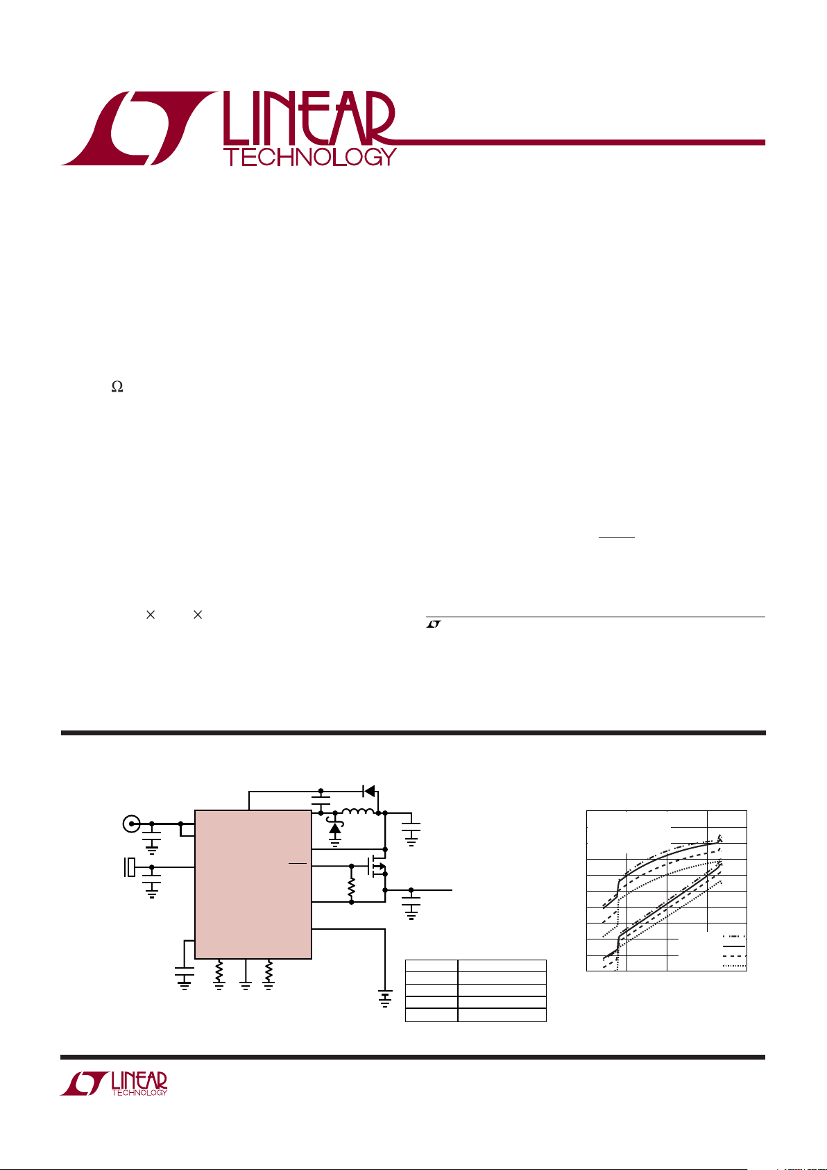
TYPICAL APPLICATIO
U
USB Power Manager with
High Voltage Switching Charger
The LTC®4089/LTC4089-5 are USB power managers plus
high voltage Li-Ion battery chargers. These devices control
the total current used by the USB peripheral for operation
and battery charging. Battery charge current is automatically reduced such that the sum of the load current and
the charge current does not exceed the programmed input
current limit. The LTC4089/LTC4089-5 also accommodate
high voltage power supplies, such as 12V AC-DC wall
adapters, FireWire, or automotive power.
The LTC4089 provides an adaptive output that tracks the
battery voltage for high effi ciency charging from the high
voltage input. The LTC4089-5 provides a fi xed 5V output
from the high voltage input to charge single cell Li-Ion
batteries. The charge current is programmable and an
end-of-charge status output (CHRG) indicates full charge.
Also featured is programmable total charge time, an NTC
thermistor input used to monitor battery temperature while
charging and automatic recharging of the battery.
■
Portable USB Devices—GPS Receivers, Cameras,
MP3 Players, PDAs
■
Seamless Transition Between Power Sources: Li-Ion
Battery, USB, and 6V to 36V External Supply
■
High Effi ciency 1.2A Charger from 6V to 36V Input
with Adaptive Output Control (LTC4089)
■
Load Dependent Charging from USB Input
Guarantees Current Compliance
■
215m Internal Ideal Diode plus Optional External
Ideal Diode Controller Provides Low Loss Power
Path When External Supply/USB Not Present
■
Constant-Current/Constant-Voltage Operation with
Thermal Feedback to Maximize Charging Rate
without Risk of Overheating
■
Selectable 100% or 20% Current Limit (e.g., 500mA/
100mA) from USB Input
■
Preset 4.2V Charge Voltage with 0.8% Accuracy
■
C/10 Charge Current Detection Output
■
NTC Thermistor Input for Temperature Qualifi ed
Charging
■
Tiny (6mm 3mm 0.75mm) 22-Pin DFN Package
APPLICATIO S
U
FEATURES
DESCRIPTIO
U
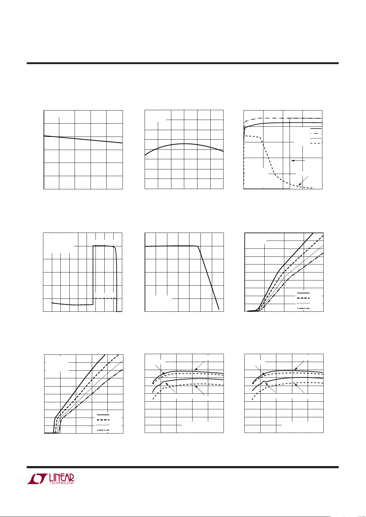
LTC4089 High Voltage
Battery Charger Effi ciency
BATTERY VOLTAGE (V)
2.5
40
EFFICIENCY (%)
45
55
60
65
90
75
3
3.5
4089 TA01b
50
80
85
70
4
4.5
HVIN = 8V
HVIN = 12V
HVIN = 24V
HVIN = 36V
CC CURRENT = 970mA
NO OUTPUT LOAD
FIGURE 10 SCHEMATIC
WITH R
PROG
= 52k
LTC4089-5
LTC4089
LTC4089/LTC4089-5
2
40895fb
Terminal Voltage
BOOST ...................................................... –0.3V to 50V
BOOST above SW .....................................................25V
HVIN, HVEN .............................................. –0.3V to 40V
IN, OUT, HVOUT
t < 1ms and Duty Cycle < 1% .................. –0.3V to 7V
DC ............................................................ –0.3V to 6V
BAT .............................................................. –0.3V to 6V
NTC, TIMER, PROG, CLPROG .......–0.3V to (V
CC
+ 0.3V)
CHRG, HPWR, SUSP, HVPR ......................... –0.3V to 6V
Pin Current, DC
IN, OUT, BAT (Note 6) ..............................................2.5A
Operating Temperature Range
LTC4089E ................................................. –40°C to 85°C
Maximum Operating Junction Temperature .......... 110°C
Storage Temperature Range ................... –65°C to 125°C
(Notes 1, 2, 3, 4, 5)
The
● denotes the specifi cations which apply over the full operating
temperature range, otherwise specifi cations are at TA = 25°C. HVIN = 12V, BOOST = 17V, VIN = 5V, V
BAT
= 3.7V, HVEN = 12V,
HPWR = 5V, R
PROG
= 100k, R
CLPROG
= 2k, SUSP = 0V, unless otherwise noted.
SYMBOL PARAMETER CONDITIONS MIN TYP MAX UNITS
USB Input Current Limit
V
IN
USB Input Supply Voltage IN
●
4.35 5.5 V
I
IN
Input Bias Current I
BAT
= 0 (Note 7)
Suspend Mode; SUSP = 5V
●
●
0.5
50
1
100
mA
µA
I
LIM
Current Limit R
CLPROG
= 2k, HPWR = 5V
R
CLPROG
= 2k, HPWR = 0V
●
●
475
90
500
100
525
110
mA
mA
I
IN(MAX)
Maximum Input Current Limit (Note 8) 2.4 A
R
ON
ON Resistance VIN to V
OUT
I
OUT
= 80mA Load 0.215
V
CLPROG
CLPROG Pin Voltage R
CLPROG
= 2k
R
CLPROG
= 1k
●
●
0.98
0.98
1.00
1.00
1.02
1.02
V
V
I
SS
Soft-Start Inrush Current IN 5 mA/µs
V
CLEN
Input Current Limit Enable
Threshold Voltage (V
IN
– V
OUT
)
(V
IN
– V
OUT
) VIN Rising
(V
IN
– V
OUT
) VIN Falling
20
–80
50
–50
80
–20
mV
mV
ELECTRICAL CHARACTERISTICS
ABSOLUTE AXI U RATI GS
W
WW
U
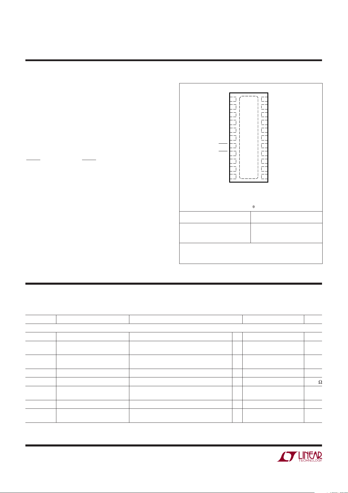
PACKAGE/ORDER I FOR ATIO
UUW
22
21
20
19
18
17
16
15
14
13
12
1
2
3
4
5
6
7
8
9
10
11
HVEN
HVIN
BOOST
SW
HVOUT
TIMER
SUSP
HPWR
CLPROG
OUT
IN
TOP VIEW
23
DJC PACKAGE
22-LEAD (6mm × 3mm) PLASTIC DFN
GND
GND
HVOUT
V
C
NTC
VNTC
HVPR
CHRG
PROG
GATE
BAT
EXPOSED PAD (PIN 23) IS GND
(MUST BE SOLDERED TO PCB)
T
JMAX
= 110°C, JA = 40°C/W
ORDER PART NUMBER DJC PART MARKING
LTC4089EDJC
LTC4089EDJC-5
4089
40895
Order Options Tape and Reel: Add #TR
Lead Free: Add #PBF Lead Free Tape and Reel: Add #TRPBF
Lead Free Part Marking: http://www.linear.com/leadfree/
Consult LTC Marketing for parts specifi ed with wider operating temperature ranges.
LTC4089/LTC4089-5
3
40895fb
SYMBOL PARAMETER CONDITIONS MIN TYP MAX UNITS
V
UVLO
Input Undervoltage Lockout VIN Powers Part, Rising Threshold
●
3.6 3.8 4 V
dV
UVLO
Input Undervoltage Lockout
Hysteresis
VIN Rising – VIN Falling 130 mV
High Voltage Regulator
V
HVIN
HVIN Supply Voltage 6 36 V
I
HVIN
HVIN Bias Current Not Switching
Shutdown; HVEN = 0V
1.9
0.01
2.5
2
mA
µA
V
OUT
Output Voltage with HVIN Present Assumes HVOUT to OUT Connection (LTC4089)
Assumes HVOUT to OUT Connection (LTC4089-5)
●
3.45
4.85
V
BAT
+0.354.6
5.15
V
V
V
HVUVLO
High Voltage Input Undervoltage
Lockout
V
HVIN
Rising 4.7 5 V
f
SW
Switching Frequency V
HVOUT
> 3.95V
V
HVOUT
= 0V
685 750
35
815 kHz
kHz
DC
MAX
Maximum Duty Cycle
●
88 95 %
I
SW(MAX)
Switch Current Limit (Note 9) 1.5 1.95 2.3 A
V
SAT
Switch V
CESAT
ISW = 1A 330 mV
I
LK
Switch Leakage Current 2µA
V
SWD
Minimum Boost Voltage Above SW ISW = 1A 1.85 2.2 V
I
BST
BOOST Pin Current ISW = 1A 30 50 mA
Battery Management
V
BAT
Input Voltage BAT 4.3 V
I
BAT
Battery Drain Current V
BAT
= 4.3V, Charging Stopped
Suspend Mode; SUSP = 5V
V
HVIN
= VIN = 0V, BAT Powers OUT, No Load
●
●
●
15
22
60
27
35
100
µA
µA
µA
V
FLOAT
Regulated Output Voltage I
BAT
= 2mA
I
BAT
= 2mA; (0°C – 85°C)
4.165
4.158
4.200
4.200
4.235
4.242
V
V
I
CHG
Current Mode Charge Current R
PROG
= 100k, No Load
R
PROG
= 50k, No Load; (0°C – 85°C)
●
465
900
500
1000
535
1080
mA
mA
I
CHG(MAX)
Maximum Charge Current (Note 8) 1.2 A
V
PROG
PROG Pin Voltage R
PROG
= 100k
R
PROG
= 50k
●
●
0.98
0.98
1.00
1.00
1.02
1.02
V
V
k
EOC
Ratio of End-of-Charge Current to
Charge Current
V
BAT
= V
FLOAT
(4.2V)
●
0.085 0.1 0.11 mA/mA
I
TRIKL
Trickle Charge Current V
BAT
= 2V, R
PROG
= 100k 35 50 60 mA
V
TRIKL
Trickle Charge Threshold Voltage
●
2.75 2.9 3 V
V
CEN
Charger Enable Threshold Voltage (V
OUT
– V
BAT
) Falling; V
BAT
= 4V
(V
OUT
– V
BAT
) Rising; V
BAT
= 4V
55
80
mV
mV
V
RECHRG
Recharge Battery Threshold Voltage V
FLOAT
- V
RECHRG
●
65 100 135 mV
t
TIMER
TIMER Accuracy V
BAT
= 4.3V –10 10 %
Recharge Time Percent of Total Charge Time 50 %
Low Battery Trickle Charge Time Percent of Total Charge Time, V
BAT
< 2.8V 25 %
T
LIM
Junction Temperature in Constant
Temperature Mode
105 °C
The ● denotes the specifi cations which apply over the full operating
temperature range, otherwise specifi cations are at T
A
= 25°C. HVIN = 12V, BOOST = 17V, VIN = 5V, V
BAT
= 3.7V, HVEN = 12V,
HPWR = 5V, R
PROG
= 100k, R
CLPROG
= 2k, SUSP = 0V, unless otherwise noted.
ELECTRICAL CHARACTERISTICS
LTC4089/LTC4089-5
4
40895fb
SYMBOL PARAMETER CONDITIONS MIN TYP MAX UNITS
Internal Ideal Diode
R
FWD
Incremental Resistance, VON
Regulation
I
BAT
= 100mA 125
m
R
DIO,ON
ON Resistance V
BAT
to V
OUT
I
BAT
= 600mA 215
m
V
FWD
Voltage Forward Drop (V
BAT
- V
OUT
)I
BAT
= 5mA
I
BAT
= 100mA
I
BAT
= 600mA
●
10 30
55
160
50 mV
mV
mV
V
OFF
Diode Disable Battery Voltage 2.8 V
I
FWD
Load Current Limit, for VON
Regulation
550 mA
I
D(MAX)
Diode Current Limit 2.2 A
External Ideal Diode
V
FWD, EXT
External Diode Forward Voltage 20 mV
Logic
V
OL
Output Low Voltage (CHRG, HVPR) I
SINK
= 5mA
●
0.1 0.4 V
V
IH
Input High Voltage HVEN, SUSP, HPWR Pin Low to High 2.3 V
V
IL
Input Low Voltage HVEN, SUSP, HPWR Pin High to Low 0.3 V
I
PULLDN
Logic Input Pull Down Current SUSP, HPWR 2 µA
I
HVEN
HVEN Pin Bias Current V
HVEN
= 2.3V
V
HVEN
= 0V
6
0.01
20
0.1
µA
µA
V
CHG,SD
Charger Shutdown Threshold
Voltage on TIMER
●
0.14 0.4 V
I
CHG,SD
Charger Shutdown Pull-Up Current
on TIMER
V
TIMER
= 0V
●
514 µA
NTC
I
VNTC
VNTC Pin Current V
VNTC
= 2.5V
●
1.4 2.5 3.5 mA
V
VNTC
VNTC Bias Voltage I
VNTC
= 500µA
●
4.4 4.85 V
I
NTC
NTC Input Leakage Current V
NTC
= 1V 0
±1
µA
V
COLD
Cold Temperature Fault Threshold
Voltage
Rising Threshold
Hysteresis
0.74•V
VNTC
0.02•V
VNTC
V
V
V
HOT
Hot Temperature Fault Threshold
Voltage
Falling Threshold
Hysteresis
0.29•V
VNTC
0.01•V
VNTC
V
V
V
DIS
NTC Disable Voltage NTC Input Voltage to GND (Falling)
Hysteresis
●
75 100
35
125 mV
mV
The ● denotes the specifi cations which apply over the full operating
temperature range, otherwise specifi cations are at T
A
= 25°C. HVIN = 12V, BOOST = 17V, VIN = 5V, V
BAT
= 3.7V, HVEN = 12V,
HPWR = 5V, R
PROG
= 100k, R
CLPROG
= 2k, SUSP = 0V, unless otherwise noted.
ELECTRICAL CHARACTERISTICS
Note 1: Stresses beyond those listed under Absolute Maximum Ratings
may cause permanent damage to the device. Exposure to any Absolute
Maximum Rating condition for extended periods may affect device
reliability and lifetime.
Note 2: V
CC
is the greater of VIN, V
OUT
or V
BAT
Note 3: All voltage values are with respect to GND.
Note 4: This IC includes over-temperature protection that is intended
to protect the device during momentary overload conditions. Junction
temperatures will exceed 110°C when over-temperature protection is
active. Continuous operation above the specifi ed maximum operating
junction temperature may result in device degradation or failure.
Note 5: The LTC4089/LTC4089-5 are guaranteed to meet specifi ed
performance from 0°C to 85°C and are designed, characterized and
expected to meet these extended temperature limits, but are not tested
at –40°C and 85°C.
Note 6: Guaranteed by long term current density limitations.
Note 7: Total input current is equal to this specifi cation plus 1.002 • I
BAT
where I
BAT
is the charge current.
Note 8: Accuracy of programmed current may degrade for currents greater
than 1.5A.
Note 9: Current limit guaranteed by design and/or correlation to static test.
Slope compensation reduces current limit at high duty cycle.
LTC4089/LTC4089-5
5
40895fb
TIME (MIN)
0
V
BAT
, V
OUT
, V
CHRGB
(V)
I
BAT
(mA)
2
3
200
40895 G03
1
0
50
100
150
5
4
600
900
300
0
1500
1200
V
BAT
V
OUT
V
CHRGB
I
BAT
1250mAh
CELL
HVIN = 12V
R
PROG
= 50k
C/10
TERMINATION
I
BAT
(mA)
0
4.00
V
FLOAT
(V)
4.05
4.10
4.15
4.20
4.25
4.30
200 400 600 800
40895 G01
1000
R
PROG
= 34k
TEMPERATURE (°C)
–50
V
FLOAT
(V)
4.195
4.200
4.205
25
75
40895 G02
4.190
4.185
4.180
–25 0 50
4.210
4.215
4.220
100
VIN = 5V
I
BAT
= 2mA
V
BAT
(V)
0
0
I
BAT
(mA)
100
300
400
500
1
2
2.5 4.5
40895 G04
200
0.5 1.5
3
3.5
4
600
VIN = 5V
V
OUT
= NO LOAD
R
PROG
= 100k
R
CLPROG
= 2k
HPWR = 5V
HPWR = 0V
TEMPERATURE (°C)
–50
I
BAT
(mA)
400
500
600
25 75
40895 G05
300
200
–25 0
50 100 125
100
0
VIN = 5V
V
BAT
= 3.5V
θ
JA
= 50°C/W
V
FWD
(mV)
0
0
I
OUT
(mA)
100
300
400
500
1000
700
50
100
40895 G06
200
800
900
600
150
200
V
BAT
= 3.7V
V
IN
= 0V
–50°C
0°C
50°C
100°C
0
3000
4000
5000
80
4085 G17
2000
1000
2500
3500
4500
1500
500
0
20
40
60
100
V
FWD
(mV)
I
OUT
(mA)
V
BAT
= 3.7V
V
IN
= 0V
Si2333 PFET
–50°C
0°C
50°C
100°C
I
OUT
(A)
0
EFFICIENCY (%)
80
90
100
0.8
40895 G08
70
60
75
85
95
65
55
50
0.2
0.4
0.6
1.0
FIGURE 10 SCHEMATIC
V
BAT
= 4.21V (I
BAT
= 0)
HVIN = 8V
HVIN = 12V
HVIN = 36V
HVIN = 24V
I
OUT
(A)
0
EFFICIENCY (%)
80
90
100
0.8
40895 G09
70
60
75
85
95
65
55
50
0.2
0.4
0.6
1.0
FIGURE 10 SCHEMATIC
V
BAT
= 4.21V (I
BAT
= 0)
HVIN = 8V
HVIN = 12V
HVIN = 36V
HVIN = 24V
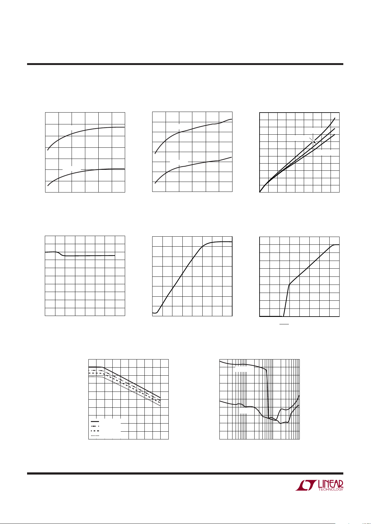
TYPICAL PERFORMANCE CHARACTERISTICS
V
FLOAT
Load Regulation
Battery Regulation (Float)
Voltage vs Temperature
Battery Current and Voltage vs
Time (LTC4089)
Charging from USB, I
BAT
vs V
BAT
Charge Current vs Temperature
(Thermal Regulation)
Ideal Diode Current vs Forward
Voltage and Temperature (No
External Device)
Ideal Diode Current vs Forward
Voltage and Temperature with
External Device
LTC4089 High Voltage Regulator
Effi ciency vs Output Load
LTC4089-5 High Voltage
Regulator Effi ciency vs Output
Load
T
A
= 25°C, unless otherwise specifi ed.
LTC4089/LTC4089-5
6
40895fb
VIN (V)
5
1.6
1.5
1.4
1.3
1.2
1.1
1.0
0.9
20 30
40895 G10
10 15
25 35
I
OUT
(A)
MINIMUM
TYPICAL
VIN (V)
5
1.8
1.6
1.5
1.4
1.3
1.2
1.1
1.0
0.9
20 30
40895 G11
10 15
25 35
I
OUT
(A)
MINIMUM
TYPICAL
SWITCH CURRENT (A)
0
V
CE(SW)
(mV)
150
450
500
550
0.4
0.8
1.0
40895 G12
50
350
250
100
400
0
300
200
0.2
0.6
1.4
1.2
1.6
1.8
TA = 25°C
TA = 85°C
TA = –40°C
TEMPERATURE (°C)
FREQUENCY (kHz)
720
760
800
125
40895 G13
680
640
700
740
780
660
620
600
–25–50
250
75 100 150
50
FEEDBACK VOLTAGE (mV)
0
SWITCHING FREQUENCY (kHz)
400
600
800
40895 G14
200
0
200
400
600
100
300
500
700
800
300
500
100
700
SHDN PIN VOLTAGE (V)
0
0
SWITCH CURRENT LIMIT (A)
0.2
0.6
0.8
1.0
2.0
1.4
0.50 1 1.25
40895 G15
0.4
1.6
1.8
1.2
0.25 0.75 1.50 1.75 2
DUTY CYCLE (%)
0
CURRENT LIMIT (A)
1.6
1.8
2.0
80
40895 G16
1.4
1.2
1.5
1.7
1.9
1.3
1.1
1.0
2010
4030
60 70 90
50
100
TA = –40°C
T
A
= –5°C
T
A
= 25°C
T
A
= 90°C
LOAD CURRENT (mA)
1
5.8
INPUT VOLTAGE (V)
6.0
6.2
6.4
6.6
10 100 1000
40895 G17
5.6
5.4
5.2
5.0
6.8
7.0
TO START
TO RUN
TYPICAL PERFORMANCE CHARACTERISTICS
High Voltage Regulator
Maximum Load Current, L = 10µH
High Voltage Regulator
Maximum Load Current, L = 33µH
High Voltage Regulator
Switch Voltage Drop
High Voltage Regulator
Switch Frequency
High Voltage Regulator
Frequency Foldback
High Voltage Regulator
Soft-Start
High Voltage Switch Current Limit
High Voltage Regulator
Typical Minimum Input Voltage
T
A
= 25°C, unless otherwise specifi ed.
LTC4089/LTC4089-5
7
40895fb
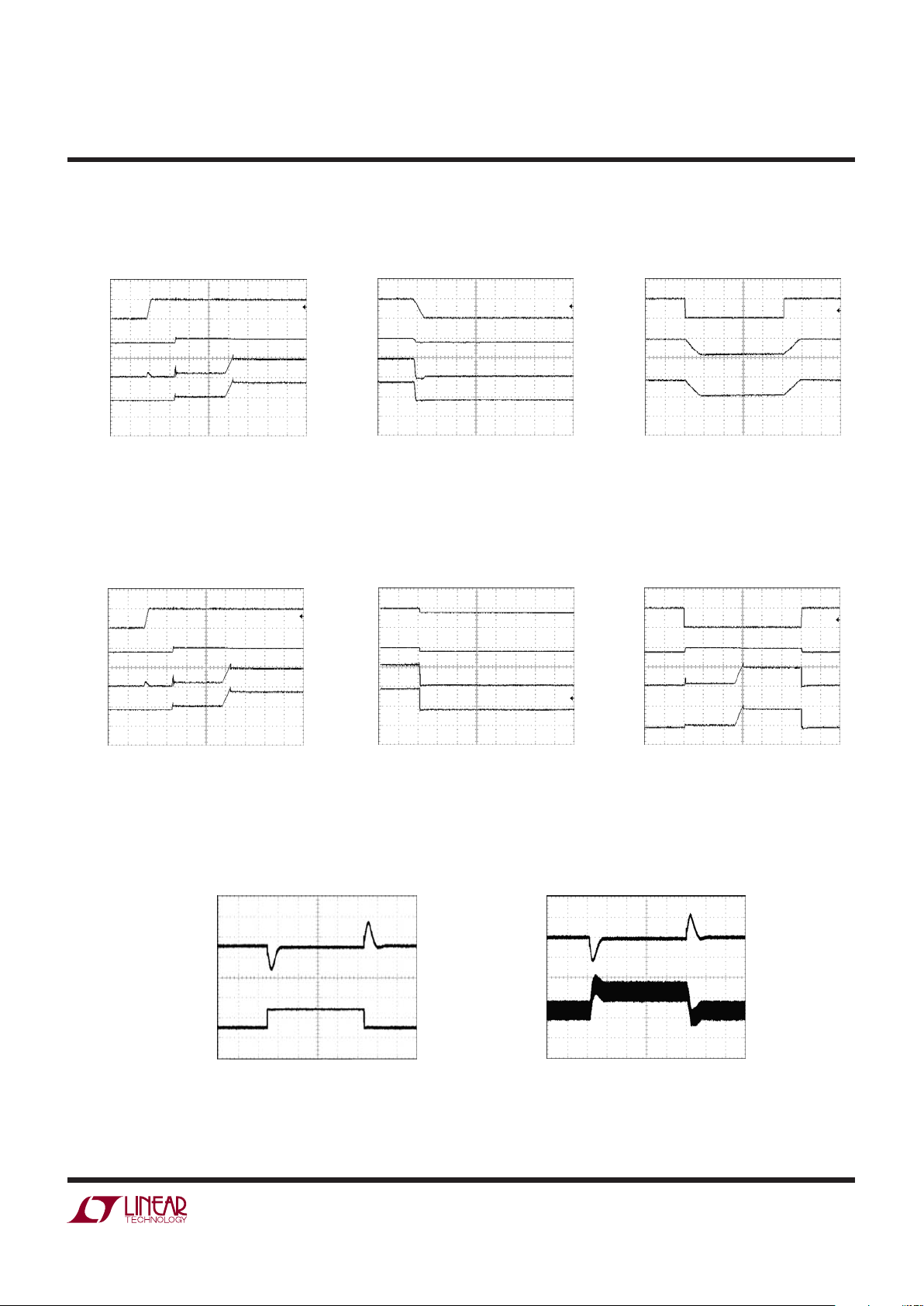
1ms/DIV
V
IN
5V/DIV
V
OUT
5V/DIV
I
IN
0.5A/DIV
I
BAT
0.5A/DIV
40895 G18
V
BAT
= 3.85V
I
OUT
= 100mA
1ms/DIV
V
IN
5V/DIV
V
OUT
5V/DIV
I
IN
0.5A/DIV
I
BAT
0.5A/DIV
40895 G19
V
BAT
= 3.85V
I
OUT
= 100mA
100µs/DIV
HPWR
5V/DIV
I
IN
0.5A/DIV
I
BAT
0.5A/DIV
40895 G20
V
BAT
= 3.85V
I
OUT
= 50mA
1ms/DIV
WALL
5V/DIV
V
OUT
5V/DIV
I
WALL
0.5A/DIV
I
BAT
0.5A/DIV
40895 G21
V
BAT
= 3.85V
I
OUT
= 100mA
R
PROG
= 100k
1ms/DIV
WALL
5V/DIV
V
OUT
5V/DIV
I
WALL
0.5A/DIV
I
BAT
0.5A/DIV
40895 G22
V
BAT
= 3.85V
I
OUT
= 100mA
R
PROG
= 100k
100µs/DIV
SUSP
5V/DIV
V
OUT
5V/DIV
I
IN
0.5A/DIV
I
BAT
0.5A/DIV
40895 G23
V
BAT
= 3.85V
I
OUT
= 50mA
20µS/DIV
H
VOUT
50mV/DIV
I
OUT
0.5A/DIV
40895 G24
20µS/DIV
H
VOUT
50mV/DIV
I
L
0.5A/DIV
40895 G25
Input Connect Waveforms
TYPICAL PERFORMANCE CHARACTERISTICS
Input Disconnect Waveforms Response to HPWR
Wall Connect Waveforms
Wall Disconnect Waveforms Response to Suspend
High Voltage Regulator Load
Transient
High Voltage Regulator Load
Transient
T
A
= 25°C, unless otherwise specifi ed.

LTC4089/LTC4089-5
8
40895fb
PI FU CTIO S
UUU
GND (Pins 1, 2): Ground. Tie the GND pin to a local ground
plane below the LTC4089 and the circuit components.
HVOUT (Pins 3, 18): Voltage Output of the High Voltage
Regulator. When suffi cient voltage is present at HVOUT,
the low voltage power path from IN to OUT will be disconnected and the HVPR pin will be pulled low to indicate
that a high voltage wall adapter has been detected. The
LTC4089 high voltage regulator will maintain just enough
differential voltage between HVOUT and BAT to keep the
battery charger MOSFET out of dropout (typically 300mV
from OUT to BAT). The LTC4089-5 high voltage regulator will provide a fi xed 5V output to the battery charger
MOSFET. HVOUT should be bypassed with at least 10µF
to GND. Connect pins 3 and 18 with a resistance no
greater than 1
.
V
C
(Pin 4): Leave the VC pin fl oating or bypass to ground
with a 10pF capacitor. This optional 10pF capacitor reduces
HVOUT ripple in discontinuous mode.
NTC (Pin 5): Input to the NTC Thermistor Monitoring
Circuits. Under normal operation, tie a thermistor from
the NTC pin to ground and a resistor of equal value from
NTC to VNTC. When the voltage on this pin is above 0.74
• V
VNTC
(Cold, 0°C) or below 0.29 • V
VNTC
(Hot, 50°C)
the timer is suspended but not cleared, the charging is
disabled and the CHRG pin remains in its former state.
When the voltage on NTC comes back between 0.74 •
V
VNTC
and 0.29 • V
VNTC
, the timer continues where it
left off and charging is re-enabled if the battery voltage
is below the recharge threshold. There is approximately
3°C of temperature hysteresis associated with each of the
input comparators.
Connect the NTC pin to ground to disable this feature. This
will disable all of the LTC4089 NTC functions.
VNTC (Pin 6): Output Bias Voltage for NTC. A resistor from
this pin to the NTC pin will bias the NTC thermistor.
HVPR (Pin 7): High Voltage Present Output. Active low
open drain output pin. A low on this pin indicates that the
high voltage regulator has suffi cient voltage to charge the
battery. This feature is disabled if no power is present on
HVIN, IN or BAT (i.e., below UVLO thresholds).
CHRG (Pin 8): Open-Drain Charge Status Output. When the
battery is being charged, the CHRG pin is pulled low by an
internal N-channel MOSFET. When the timer runs out or
the charge current drops below 10% of the programmed
charge current or the input supply is removed, the CHRG
pin is forced to a high impedance state.
PROG (Pin 9): Charge Current Program. Connecting a
resistor, R
PROG
, to ground programs the battery charge
current. The battery charge current is programmed
as follows:
IA
V
R
CHG
PROG
(),=
50 000
GATE (Pin 10): External ideal diode gate pin. This pin can
be used to drive the gate of an optional external PFET connected between BAT (drain) and OUT (source). By doing
so, the impedance of the ideal diode between BAT and
OUT can be reduced. When not in use, this pin should be
left fl oating. It is important to maintain a high impedance
on this pin and minimize all leakage paths.
BAT (Pin 11): Connect to a single cell Li-Ion battery. This
pin is used as an output when charging the battery and as
an input when supplying power to OUT. When the OUT pin
potential drops below the BAT pin potential, an ideal diode
function connects BAT to OUT and prevents V
OUT
from
dropping more than 100mV below V
BAT
. A precision internal
resistor divider sets the fi nal fl oat (charging) potential on
this pin. The internal resistor divider is disconnected when
IN and HVIN are in undervoltage lockout.
IN (Pin 12): Input Supply. Connect to USB supply, V
BUS
.
Input current to this pin is limited to either 20% or 100%
of the current programmed by the CLPROG pin as determined by the state of the HPWR pin. Charge current
(to the BAT pin) supplied through the input is set to the
current programmed by the PROG pin but will be limited
by the input current limit if charge current is set greater
than the input current limit.
 Loading...