

Linear Technology LTC4085, LTC4085EDE Datasheet
LTC4085
1
4085fa
I
LOAD
(mA)
0
600
500
400
300
200
100
0
–100
300 500
4085 TA01b
100 200
400 600
CURRENT (mA)
I
LOAD
I
IN
I
BAT
(CHARGING)
I
BAT
(DISCHARGING)
WALL = 0V
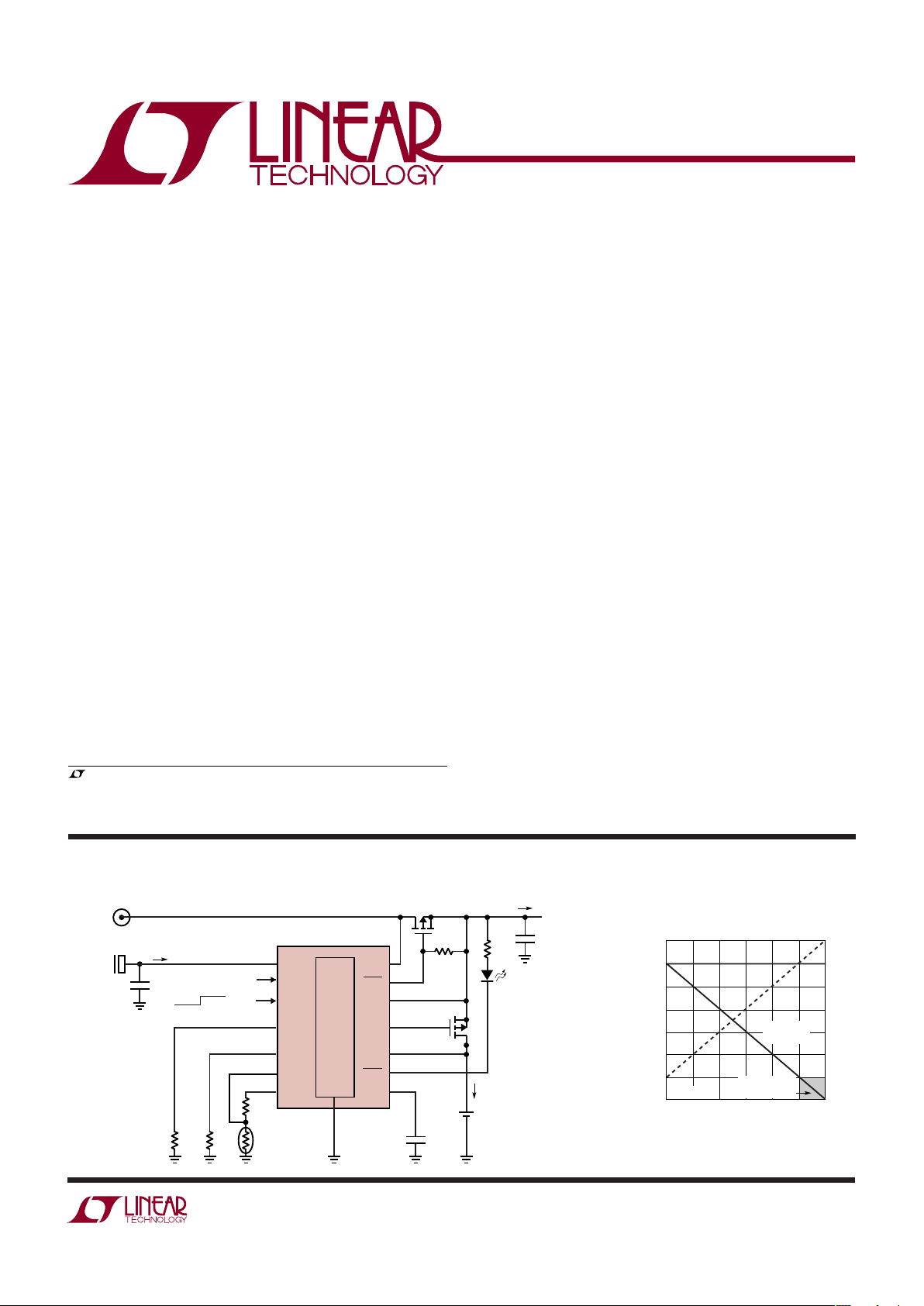
USB Power Manager with
Ideal Diode Controller and
Li-Ion Charger
The LTC®4085 is a USB power manager and Li-Ion battery
charger designed for portable battery-powered applications. The part controls the total current used by the USB
peripheral for operation and battery charging. The total
input current can be limited to 20% or 100% of a programmed value up to 1.5A (typically 100mA or 500mA).
Battery charge current is automatically reduced such that
the sum of the load current and charge current does not
exceed the programmed input current limit.
The LTC4085 includes a complete constant-current/constant-voltage linear charger for single cell Li-ion batteries.
The fl oat voltage applied to the battery is held to a tight
0.8% tolerance, and charge current is programmable using
an external resistor to ground. An end-of-charge status
output
⎯C⎯H⎯R⎯
G indicates full charge. Total charge time is
programmable by an external capacitor to ground. When
the battery drops 100mV below the fl oat voltage, automatic
recharging of the battery occurs. Also featured is an NTC
thermistor input used to monitor battery temperature
while charging.
The LTC4085 is available in a 14-lead low profi le 4mm ×
3mm DFN package.
■
Portable USB Devices: Cameras, MP3 Players, PDAs
■
Seamless Transition Between Input Power Sources:
Li-Ion Battery, USB and 5V Wall Adapter
■
215mΩ Internal Ideal Diode Plus Optional External
Ideal Diode Controller Provide Low Loss PowerPath
TM
When Wall Adapter/USB Input Not Present
■
Load Dependent Charging Guarantees Accurate USB
Input Current Compliance
■
Constant-Current/Constant-Voltage Operation with
Thermal Feedback to Maximize Charging Rate Without
Risk of Overheating*
■
Selectable 100% or 20% Input Current Limit
(e.g., 500mA/100mA)
■
Battery Charge Current Independently Programmable
Up to 1.2A
■
Preset 4.2V Charge Voltage with 0.8% Accuracy
■
C/10 Charge Current Detection Output
■
NTC Thermistor Input for Temperature Qualifi ed Charging
■
Tiny (4mm × 3mm × 0.75mm) 14-Lead DFN Package
APPLICATIO S
U
FEATURES DESCRIPTIO
U
TYPICAL APPLICATIO
U
IN
SUSP
HPWR
PROG
CLPROG
NTC
V
NTC
WALL
ACPR
OUT
GATE
BAT
CHRG
TIMER
LTC4085
GND
+
0.1µF
4.7µF
TO LDOs,
REGs, ETC
10k
10k2k100k
5V WALL
ADAPTER
INPUT
5V (NOM)
FROM USB
CABLE V
BUS
4.7µF
SUSPEND USB POWER
100mA 500mA SELECT
1k
510Ω
4085 TA01
*
* OPTIONAL - TO LOWER
IDEAL DIODE IMPEDANCE
I
IN
I
LOAD
I
BAT
, LT, LTC and LTM are registered trademarks of Linear Technology Corporation.
PowerPath is a trademark of Linear Technology Corporation. All other trademarks are the
property of their respective owners. Protected by U.S. Patents, including 6522118, 6700364.
Other patents pending.
Input and Battery Current vs Load Current
R
PROG
= 100k, R
CLPROG
= 2k
LTC4085
2
4085fa
(Notes 1, 2, 3, 4, 5)
Terminal Voltage
IN, OUT
t < 1ms and Duty Cycle < 1% ................... –0.3V to 7V
Steady State ............................................. –0.3V to 6V
BAT,
⎯C⎯H⎯R⎯
G, HPWR, SUSP, WALL, ⎯A⎯C⎯P⎯R ..... –0.3V to 6V
NTC, TIMER, PROG, CLPROG .......–0.3V to (V
CC
+ 0.3V)
Pin Current (Steady State)
IN, OUT, BAT (Note 6) ..............................................2.5A
Operating Temperature Range ................. –40°C to 85°C
Maximum Operating Junction Temperature .......... 110°C
Storage Temperature Range ................... –65°C to 125°C
The
●
indicates specifi cations which apply over the full operating
temperature range, otherwise specifi cations are at TA = 25°C. VIN = 5V, V
BAT
= 3.7V, HPWR = 5V, WALL = 0V, R
PROG
= 100k,
R
CLPROG
= 2k, unless otherwise noted.
SYMBOL PARAMETER CONDITIONS MIN TYP MAX UNITS
V
IN
Input Supply Voltage IN and OUT
4.35 5.5 V
V
BAT
Input Voltage BAT
4.3 V
I
IN
Input Supply Current I
BAT
= 0 (Note 7)
Suspend Mode; SUSP = 5V
Suspend Mode; SUSP = 5V, WALL = 5V,
V
OUT
= 4.8V
●
●
●
0.5
50
60
1.2
100
110
mA
μA
μA
I
OUT
Output Supply Current V
OUT
= 5V, VIN = 0V, NTC = V
NTC
●
0.7 1.4 mA
I
BAT
Battery Drain Current V
BAT
= 4.3V, Charging Stopped
Suspend Mode; SUSP = 5V
V
IN
= 0V, BAT Powers OUT, No Load
●
●
●
15
22
60
27
35
100
μA
μA
μA
V
UVLO
Input or Output Undervoltage Lockout VIN Powers Part, Rising Threshold
V
OUT
Powers Part, Rising Threshold
●
●
3.6
2.75
3.8
2.9543.15
V
V
ΔV
UVLO
Input or Output Undervoltage Lockout VIN Rising – VIN Falling
or V
OUT
Rising – V
OUT
Falling
130 mV
Current Limit
I
LIM
Current Limit R
CLPROG
= 2k (0.1%), HPWR = 5V
R
CLPROG
= 2k (0.1%), HPWR = 0V
●
●
475
90
500
100
525
110
mA
mA
I
IN(MAX)
Maximum Input Current Limit (Note 8) 2.4 A
R
ON
ON Resistance VIN to V
OUT
I
OUT
= 100mA Load 215 mΩ
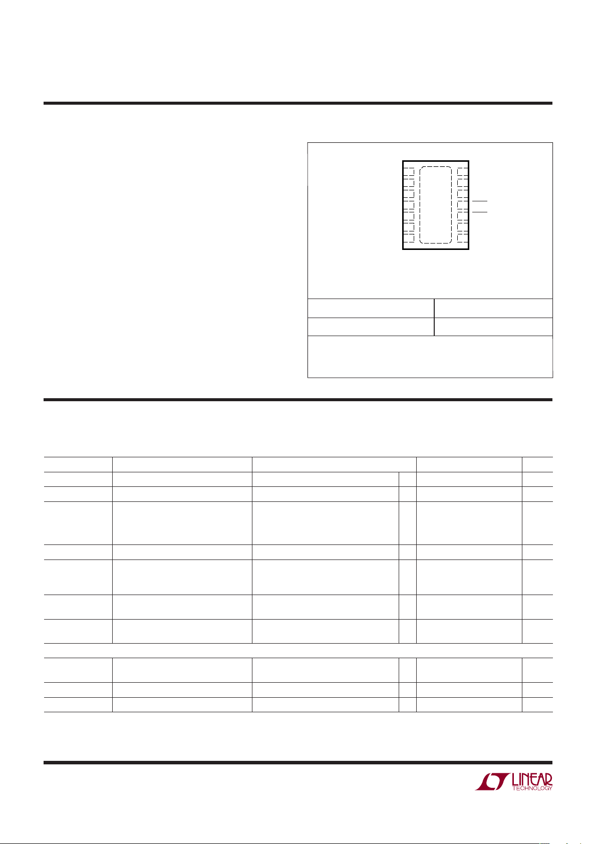
ELECTRICAL CHARACTERISTICS
ABSOLUTE AXI U RATI GS
W
WW
U
ORDER PART NUMBER
DE PART MARKING
Consult LTC Marketing for parts specifi ed with wider operating temperature ranges.
4085
PACKAGE/ORDER I FOR ATIO
UUW
T
JMAX
= 125°C, θJA = 40°C/W
EXPOSED PAD (PIN 15) IS GND, MUST BE CONNECTED TO PCB
Order Options Tape and Reel: Add #TR
Lead Free: Add #PBF Lead Free Tape and Reel: Add #TRPBF
Lead Free Part Marking: http://www.linear.com/leadfree/
1
2
3
4
5
6
7
14
13
12
11
10
9
8
BAT
GATE
PROG
CHRG
ACPR
V
NTC
NTC
IN
OUT
CLPROG
HPWR
SUSP
TIMER
WALL
TOP VIEW
15
DE PACKAGE
14-LEAD (4mm × 3mm) PLASTIC DFN
LTC4085EDE
LTC4085
3
4085fa
SYMBOL PARAMETER CONDITIONS MIN TYP MAX UNITS
V
CLPROG
CLPROG Pin Voltage R
PROG
= 2k
R
PROG
= 1k
●
●
0.98
0.98
1
1
1.02
1.02
V
V
I
SS
Soft Start Inrush Current IN or OUT 5 mA/μs
V
CLEN
Input Current Limit Enable Threshold
Voltage
(VIN – V
OUT
) VIN Rising
(V
IN
– V
OUT
) VIN Falling
20
-80
50
-60
80
-20
mV
mV
Battery Charger
V
FLOAT
Regulated Output Voltage I
BAT
= 2mA
I
BAT
= 2mA, (0°C – 85°C)
4.165
4.158
4.2
4.2
4.235
4.242
V
V
I
BAT
Current Mode Charge Current R
PROG
= 100k (0.1%), No Load
R
PROG
= 50k (0.1%), No Load
●
●
465
920
500
1000
535
1080
mA
mA
I
BAT(MAX)
Maximum Charge Current (Note 8) 1.5 A
V
PROG
PROG Pin Voltage R
PROG
= 100k
R
PROG
= 50k
●
●
0.98
0.98
1
1
1.02
1.02
V
V
k
EOC
Ratio of End-of-Charge Current to
Charge Current
V
BAT
= V
FLOAT
(4.2V)
●
0.085 0.1 0.11 mA/mA
I
TRIKL
Trickle Charge Current V
BAT
= 2V, R
PROG
= 100k (0.1%) 40 50 60 mA
V
TRIKL
Trickle Charge Threshold Voltage
●
2.8 2.9 3 V
V
CEN
Charger Enable Threshold Voltage (V
OUT
– V
BAT
) Falling; V
BAT
= 4V
(V
OUT
– V
BAT
) Rising; V
BAT
= 4V
55
80
mV
mV
V
RECHRG
Recharge Battery Threshold Voltage V
FLOAT
– V
RECHRG
●
60 100 130 mV
t
TIMER
TIMER Accuracy V
BAT
= 4.3V -10 10 %
Recharge Time Percent of Total Charge Time 50 %
Low Battery Trickle Charge Time Percent of Total Charge Time, V
BAT
< 2.8V 25 %
T
LIM
Junction Temperature in Constant
Temperature Mode
105 °C
Internal Ideal Diode
R
FWD
Incremental Resistance, VON Regulation I
BAT
= 100mA 125 mΩ
R
DIO(ON)
ON Resistance V
BAT
to V
OUT
I
BAT
= 600mA 215 mΩ
V
FWD
Voltage Forward Drop (V
BAT
– V
OUT
)I
BAT
= 5mA
I
BAT
= 100mA
I
BAT
= 600mA
●
10 30
55
160
50 mV
mV
mV
V
OFF
Diode Disable Battery Voltage 2.8 V
I
FWD
Load Current Limit, for VON Regulation 550 mA
I
D(MAX)
Diode Current Limit 2.2 A
External Ideal Diode
V
FWD,EDA
External Ideal Diode Forward Voltage V
GATE
= 1.85V; I
GATE
= 0 20 mV
Logic
V
OL
Output Low Voltage ⎯C⎯H⎯R⎯G, ⎯A⎯C⎯P⎯RI
SINK
= 5mA
●
0.1 0.25 V
V
IH
Input High Voltage SUSP, HPWR Pin
●
1.2 V
V
IL
Input Low Voltage SUSP, HPWR Pin
●
0.4 V
I
PULLDN
Logic Input Pull-Down Current SUSP, HPWR 2 μA
The
●
indicates specifi cations which apply over the full operating
temperature range, otherwise specifi cations are at T
A
= 25°C. VIN = 5V, V
BAT
= 3.7V, HPWR = 5V, WALL = 0V, R
PROG
= 100k,
R
CLPROG
= 2k, unless otherwise noted.
ELECTRICAL CHARACTERISTICS
LTC4085
4
4085fa
SYMBOL PARAMETER CONDITIONS MIN TYP MAX UNITS
V
CHG(SD)
Charger Shutdown Threshold Voltage
on TIMER
●
0.15 0.4 V
I
CHG(SD)
Charger Shutdown Pull-Up Current
on TIMER
V
TIMER
= 0V
●
514 μA
V
WAR
Absolute Wall Input Threshold Voltage V
WALL
Rising Threshold
●
4.15 4.25 4.35 V
V
WAF
Absolute Wall Input Threshold Voltage V
WALL
Falling Threshold 3.12 V
V
WDR
Delta Wall Input Threshold Voltage V
WALL
– V
BAT
Rising Threshold 75 mV
V
WDF
Delta Wall Input Threshold Voltage V
WALL
– V
BAT
Falling Threshold
●
02540 mV
I
WALL
Wall Input Current V
WALL
= 5V 75 150 μA
NTC
V
VNTC
V
NTC
Bias Voltage I
VNTC
= 500μA
●
4.4 4.85 V
I
NTC
NTC Input Leakage Current V
NTC
= 1V 0 ±1 μA
V
COLD
Cold Temperature Fault Threshold
Voltage
Rising Threshold
Hysteresis
0.74 • V
VNTC
0.02 • V
VNTC
V
V
V
HOT
Hot Temperature Fault Threshold
Voltage
Falling Threshold
Hysteresis
0.29 • V
VNTC
0.01 • V
VNTC
V
V
V
DIS
NTC Disable Voltage NTC Input Voltage to GND (Falling)
Hysteresis
●
75 100
35
125 mV
mV
Note 1: Stresses beyond those listed under Absolute Maximum Ratings
may cause permanent damage to the device. Exposure to any Absolute
Maximum Rating condition for extended periods may affect device
reliability and lifetime.
Note 2: V
CC
is the greater of VIN, V
OUT
or V
BAT
.
Note 3: All voltage values are with respect to GND.
Note 4: This IC includes overtemperature protection that is intended
to protect the device during momentary overload conditions. Junction
temperatures will exceed 125°C when overtemperature protection is
active. Continuous operation above the specifi ed maximum operating
junction temperature may result in device degradation or failure.
Note 5: The LTC4085E is guaranteed to meet specifi ed performance from
0° to 85°C. Specifi cations over the –40°C to 85°C operating temperature
range are assured by design, characterization and correlation with
statistical process controls.
Note 6: Guaranteed by long term current density limitations.
Note 7: Total input current is equal to this specifi cation plus 1.002 • I
BAT
where I
BAT
is the charge current.
Note 8: Accuracy of programmed current may degrade for currents greater
than 1.5A.
The
●
indicates specifi cations which apply over the full operating
temperature range, otherwise specifi cations are at T
A
= 25°C. VIN = 5V, V
BAT
= 3.7V, HPWR = 5V, WALL = 0V, R
PROG
= 100k,
R
CLPROG
= 2k, unless otherwise noted.
ELECTRICAL CHARACTERISTICS
LTC4085
5
4085fa
TEMPERATURE (°C)
–50
V
PROG
(V)
0.995
1.000
1.005
25
75
4085 G07
0.990
0.985
0.980
–25 0 50
1.010
1.015
1.020
100
VIN = 5V
V
BAT
= 4.2V
R
PROG
= 100k
R
CLPROG
= 2k
I
BAT
(mA)
0
4.00
V
FLOAT
(V)
4.05
4.10
4.15
4.20
4.25
4.30
200 400 600 800
4085 G08
1000
R
PROG
= 34k
TEMPERATURE (°C)
–50
VFLOAT (V)
4.195
4.200
4.205
25
75
4085 G09
4.190
4.185
4.180
–25 0 50
4.210
4.215
4.220
100
VIN = 5V
I
BAT
= 2mA
TEMPERATURE (°C)
–50
0
I
IN
(µA)
100
300
400
500
50
900
4085 G01
200
0
–25
75
25 100
600
700
800
VIN = 5V
V
BAT
= 4.2V
R
PROG
= 100k
R
CLPROG
= 2k
TEMPERATURE (°C)
–50
70
60
50
40
30
20
10
0
25 75
4085 G02
25 0
50 100
I
IN
(µA)
VIN = 5V
V
BAT
= 4.2V
R
PROG
= 100k
R
CLPROG
= 2k
SUSP = 5V
TEMPERATURE (°C)
–50
0
I
BAT
(µA)
20
40
60
–25
0
25 50
4085 G03
75
80
100
10
30
50
70
90
100
VIN = 0V
V
BAT
= 4.2V
TEMPERATURE (°C)
–50
475
I
IN
(mA)
485
495
505
515
525
–25
02550
4085 G04
75 100
VIN = 5V
V
BAT
= 3.7V
R
PROG
= 100k
R
CLPROG
= 2k
TEMPERATURE (°C)
–50
I
IN
(mA)
92
96
100
–25
0
25 50
4085 G05
75
104
108
110
90
94
98
102
106
100
VIN = 5V
V
BAT
= 3.7V
R
PROG
= 100k
R
CLPROG
= 2k
TEMPERATURE (°C)
–50
0
V
CLPROG
(V)
0.2
0.4
0.6
0.8
1.2
–25
02550
4085 G06
75 100
1.0
VIN = 5V
R
CLPROG
= 2k
HPWR = 5V
HPWR = 0V
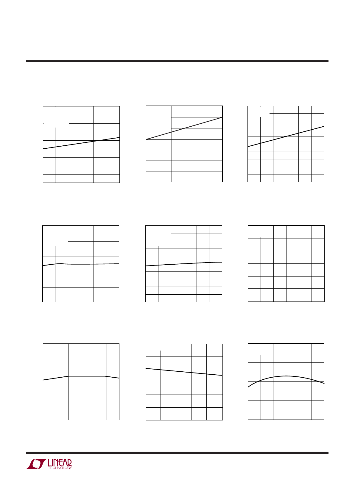
Input Supply Current
vs Temperature
Input Supply Current vs
Temperature (Suspend Mode)
Battery Drain Current
vs Temperature
(BAT Powers OUT, No Load)
Input Current Limit
vs Temperature, HPWR = 5V
Input Current Limit
vs Temperature, HPWR = 0V
CLPROG Pin Voltage
vs Temperature
PROG Pin Voltage
vs Temperature V
FLOAT
Load Regulation
Battery Regulation (Float)
Voltage vs Temperature
TYPICAL PERFOR A CE CHARACTERISTICS
UW
TA = 25°C unless otherwise noted.
LTC4085
6
4085fa
TEMPERATURE (°C)
–50
I
BAT
(mA)
400
500
600
25 75
4085 G12
300
200
–25 0
50 100 125
100
0
VIN = 5V
V
BAT
= 3.5V
θ
JA
= 50°C/W
TEMPERATURE (°C)
–50
125
R
ON
(mΩ)
150
175
200
225
275
–25
02550
4085 G10
75 100
250
VIN = 4.5V
VIN = 5.5V
I
LOAD
= 400mA
VIN = 5V
TIME (min)
0
0
I
BAT
(mA)
100
200
300
400
500
600
0
V
BAT
AND V
CHRG
(V)
1
2
3
4
5
6
50 100 150 200
4085 G11
400mAhr CELL
V
IN
= 5V
R
PROG
= 100k
R
CLPROG
= 2.1k
C/10
TERMINATION
CHRG
V
BAT
I
BAT
V
BAT
(V)
0
0
I
BAT
(mA)
100
300
400
500
1
2
2.5 4.5
4085 G13
200
0.5 1.5
3
3.5
4
600
VIN = 5V
V
OUT
= NO LOAD
R
PROG
= 100k
R
CLPROG
= 2k
HPWR = 5V
V
BAT
(V)
0
0
I
BAT
(mA)
20
60
80
100
1
2
2.5 4.5
4085 G14
40
0.5 1.5
3
3.5
4
120
VIN = 5V
V
OUT
= NO LOAD
R
PROG
= 100k
R
CLPROG
= 2k
HPWR = 0V
V
FWD
(mV)
0
0
I
OUT
(mA)
100
300
400
500
1000
700
50
100
4085 G15
200
800
900
600
150
200
V
BAT
= 3.7V
V
IN
= 0V
–50°C
0°C
50°C
100°C
V
FWD
(mV)
0
0
I
OUT
(mA), R
DIO
(mΩ)
100
300
400
500
1000
700
50
100
4085 G16
200
800
900
600
150
200
V
BAT
= 3.7V
V
IN
= 0V
R
DIO
I
OUT
0
3000
4000
5000
80
4085 G17
2000
1000
2500
3500
4500
1500
500
0
20
40
60
100
V
FWD
(mV)
I
OUT
(mA)
V
BAT
= 3.7V
V
IN
= 0V
Si2333 PFET
–50°C
0°C
50°C
100°C
0
3000
4000
5000
80
2000
1000
2500
3500
4500
1500
500
0
20
40
60
100
V
FWD
(mV)
I
OUT
(mA)
V
BAT
= 3.7V
V
IN
= 0V
Si2333 PFET
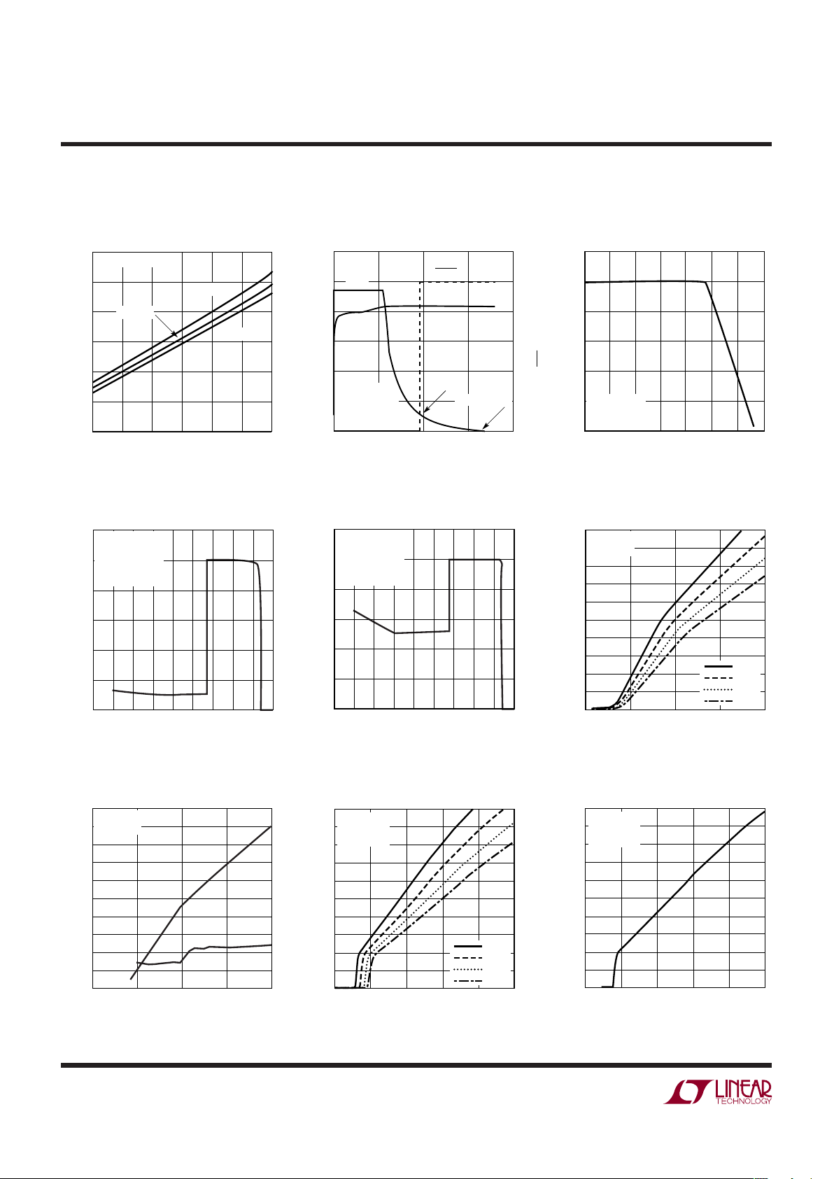
Input RON vs Temperature
Battery Current and Voltage
vs Time
Charge Current vs Temperature
(Thermal Regulation)
Charging from USB, I
BAT
vs V
BAT
Charging from USB, Low Power,
I
BAT
vs V
BAT
Ideal Diode Current vs Forward
Voltage and Temperature
(No External Device)
Ideal Diode Resistance and
Current vs Forward Voltage
(No External Device)
Ideal Diode Current vs Forward
Voltage and Temperature with
External Device
Ideal Diode Resistance and
Current vs Forward Voltage with
External Device
TYPICAL PERFOR A CE CHARACTERISTICS
UW
TA = 25°C unless otherwise noted.
LTC4085
7
4085fa
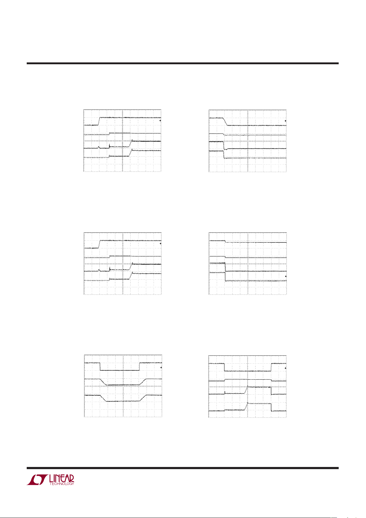
Input Connect Waveforms
Input Disconnect Waveforms
Response to HPWR
Wall Connect Waveforms,
V
IN
= 0V
TYPICAL PERFOR A CE CHARACTERISTICS
UW
TA = 25°C unless otherwise noted.
1ms/DIV
V
IN
5V/DIV
V
OUT
5V/DIV
I
IN
0.5A/DIV
I
BAT
0.5A/DIV
4085 G19
V
BAT
= 3.85V
I
OUT
= 100mA
1ms/DIV
V
IN
5V/DIV
V
OUT
5V/DIV
I
IN
0.5A/DIV
I
BAT
0.5A/DIV
4085 G20
V
BAT
= 3.85V
I
OUT
= 100mA
100µs/DIV
HPWR
5V/DIV
I
IN
0.5A/DIV
I
BAT
0.5A/DIV
4085 G21
V
BAT
= 3.85V
I
OUT
= 50mA
1ms/DIV
WALL
5V/DIV
V
OUT
5V/DIV
I
WALL
0.5A/DIV
I
BAT
0.5A/DIV
4085 G22
V
BAT
= 3.85V
I
OUT
= 100mA
R
PROG
= 100k
1ms/DIV
WALL
5V/DIV
V
OUT
5V/DIV
I
WALL
0.5A/DIV
I
BAT
0.5A/DIV
4085 G23
V
BAT
= 3.85V
I
OUT
= 100mA
R
PROG
= 100k
100µs/DIV
SUSP
5V/DIV
V
OUT
5V/DIV
I
IN
0.5A/DIV
I
BAT
0.5A/DIV
4085 G24
V
BAT
= 3.85V
I
OUT
= 50mA
Wall Disconnect Waveforms,
V
IN
= 0V
Response to Suspend

LTC4085
8
4085fa
PI FU CTIO S
UUU
IN (Pin 1): Input Supply. Connect to USB supply, V
BUS
.
Input current to this pin is limited to either 20% or 100%
of the current programmed by the CLPROG pin as determined by the state of the HPWR pin. Charge current (to
BAT pin) supplied through the input is set to the current
programmed by the PROG pin but will be limited by the
input current limit if charge current is set greater than the
input current limit.
OUT (Pin 2): Voltage Output. This pin is used to provide
controlled power to a USB device from either USB V
BUS
(IN) or the battery (BAT) when the USB is not present.
This pin can also be used as an input for battery charging
when the USB is not present and a wall adapter is applied
to this pin. OUT should be bypassed with at least 4.7μF
to GND.
CLPROG (Pin 3): Current Limit Program and Input Current Monitor. Connecting a resistor, R
CLPROG
, to ground
programs the input to output current limit. The current
limit is programmed as follows:
IA
V
R
CL
CLPROG
()=
1000
In USB applications the resistor R
CLPROG
should be set
to no less than 2.1k.
The voltage on the CLPROG pin is always proportional to
the current fl owing through the IN to OUT power path.
This current can be calculated as follows:
IA
V
R
IN
CLPROG
CLPROG
() •= 1000
HPWR (Pin 4): High Power Select. This logic input is used
to control the input current limit. A voltage greater than
1.2V on the pin will set the input current limit to 100%
of the current programmed by the CLPROG pin. A voltage less than 0.4V on the pin will set the input current
limit to 20% of the current programmed by the CLPROG
pin. A 2μA pull-down is internally applied to this pin to
ensure it is low at power up when the pin is not being
driven externally.
SUSP (Pin 5): Suspend Mode Input. Pulling this pin above
1.2V will disable the power path from IN to OUT. The supply current from IN will be reduced to comply with the
USB specifi cation for suspend mode. Both the ability to
charge the battery from OUT and the ideal diode function
(from BAT to OUT) will remain active. Suspend mode will
reset the charge timer if V
OUT
is less than V
BAT
while in
suspend mode. If V
OUT
is kept greater than V
BAT
, such as
when a wall adapter is present, the charge timer will not
be reset when the part is put in suspend. A 2μA pull-down
is internally applied to this pin to ensure it is low at power
up when the pin is not being driven externally.
TIMER (Pin 6): Timer Capacitor. Placing a capacitor, C
TIMER
,
to GND sets the timer period. The timer period is:
t Hours
C R Hours
Fk
TIMER
TIMER PROG
()
••
.•
=
µ
3
0 1 100
Charge time is increased if charge current is reduced
due to undervoltage current limit, load current, thermal
regulation and current limit selection (HPWR).
Shorting the TIMER pin to GND disables the battery
charging functions.
 Loading...