

FEATURES
■
Complete Fast Charger Controller for Single,
2-, 3- or 4-Series Cell NiMH/NiCd Batteries
■
No Firmware or Microcontroller Required
■
Termination by –∆V, Maximum Voltage or
Maximum Time
■
No Sense Resistor or Blocking Diode Required
■
Automatic Recharge Keeps Batteries Charged
■
Programmable Fast Charge Current: 0.4A to 2A
■
Accurate Charge Current: ±5% at 2A
■
Fast Charge Current Programmable Beyond 2A with
External Sense Resistor
■
Automatic Detection of Battery
■
Precharge for Heavily Discharged Batteries
■
Optional Temperature Qualified Charging
■
Charge and AC Present Status Outputs Can Drive LED
■
Automatic Sleep Mode with Input Supply Removal
■
Negligible Battery Drain in Sleep Mode: <1µA
■
Manual Shutdown
■
Input Supply Range: 4.5V to 10V
■
Available in 16-Lead DFN and TSSOP Packages
U
APPLICATIO S
■
Portable Computers, Cellular Phones and PDAs
■
Medical Equipment
■
Charging Docks and Cradles
■
Portable Consumer Electronics
LTC4060
Standalone Linear NiMH/NiCd
Fast Battery Charger
U
DESCRIPTIO
The LTC®4060 is a complete fast charging system for NiMH
or NiCd batteries. Just a few external components are
needed to design a standalone linear charging system.
An external PNP transistor provides charge current that is
user programmable with a resistor. A small external capacitor sets the maximum charge time. No external current
sense resistor is needed, and no blocking diode is required.
The IC automatically senses the DC input supply and battery insertion or removal. Heavily discharged batteries are
initially charged at a C/5 rate before a fast charge is applied.
Fast charge is terminated using the – ∆V detection method.
Backup termination consists of a programmable timer and
battery overvoltage detector. An optional external NTC thermistor can be used for temperature-based qualification of
charging. An optional programmable recharge feature automatically recharges batteries after discharge.
Manual shutdown is accomplished with the SHDN pin, while
removing input power automatically puts the LTC4060 into
sleep mode. During shutdown or sleep mode, battery drain
is <1µA.
The LTC4060 is available in both low profile (0.75mm) 16pin 5mm × 3mm DFN and 16-lead TSSOP packages. Both
feature exposed metal die mount pads for optimum thermal performance.
, LTC and LT are registered trademarks of Linear Technology Corporation.
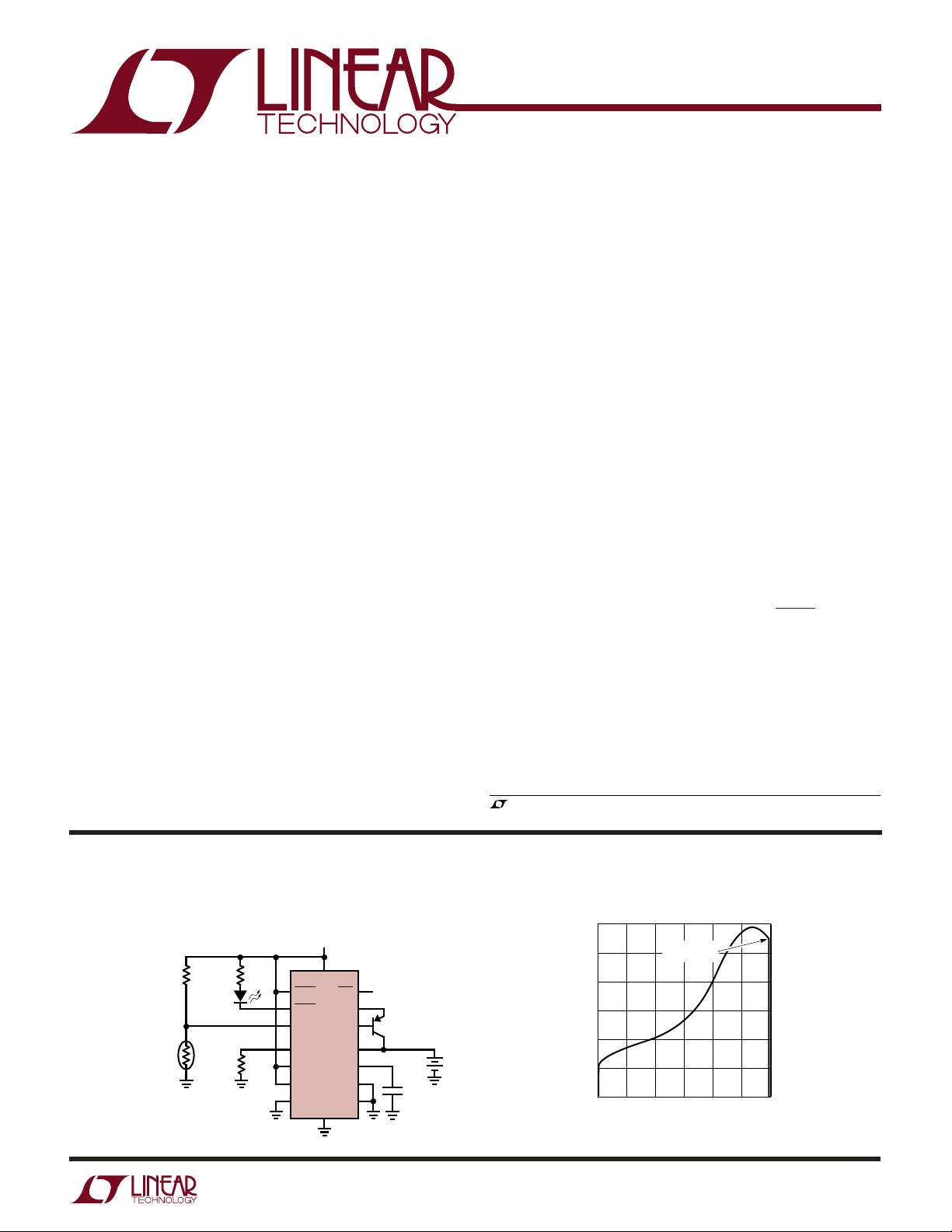
TYPICAL APPLICATIO
2-Cell, 2A Standalone NiMH Fast Charger with
Optional Thermistor and Charge Indicator
330Ω
“CHARGE”
NTC
698Ω
SHDN
CHRG
NTC
PROG
ARCT
SEL0
SEL1
U
V
IN =
V
CC
SENSE
LTC4060
PAUSE
GND
5V
ACP
DRIVE
BAT
TIMER
CHEM
1.5nF
4060 TA01
+
NiMH
BATTERY
2-Cell NiMH Charging Profile
3.40
–∆V
TERMINATION
3.30
3.20
BATTERY VOLTAGE (V)
3.10
0
10 20 30 40
CHARGE TIME (MINUTES)
50
60
4060 TA01b
4060f
1
LTC4060
WW
W
U
ABSOLUTE MAXIMUM RATINGS
(Note 1)
VCC to GND ............................................... –0.3V to 11V
Input Voltage
SHDN, NTC, SEL0, SEL1, PROG, ARCT,
BAT, CHEM, TIMER, PAUSE ...... –0.3V to VCC + 0.3V
Output Voltage
CHRG, ACP, DRIVE ................... –0.3V to VCC + 0.3V
Output Current (SENSE) ...................................... –2.2A
Short-Circuit Duration (DRIVE) ...................... Indefinite
U
W
U
PACKAGE/ORDER INFORMATION
TOP VIEW
DRIVE
1
BAT
2
SENSE
3
TIMER
4
SHDN
5
PAUSE
6
PROG
7
ARCT
8
DHC16 PACKAGE
16-LEAD (5mm × 3mm) PLASTIC DFN
T
= 125°C, θJA = 37°C/W
JMAX
EXPOSED PAD (PIN 17) IS GND
MUST BE SOLDERED TO PCB TO OBTAIN
= 37°C/W OTHERWISE θJA = 140°C
θ
JA
16
GND
15
CHRG
14
V
CC
ACP
13
17
CHEM
12
NTC
11
SEL1
10
SEL0
9
ORDER PART
NUMBER
LTC4060EDHC
DHC PART
MARKING
4060
Operating Ambient Temperature Range
(Note 2) ............................................. – 40°C to 85°C
Operating Junction Temperature (Note 3) ........... 125°C
Storage Temperature Range
TSSOP Package ............................... – 65°C to 150°C
DFN Package .................................... –65°C to 125°C
Lead Temperature (Soldering, 10 sec)
TSSOP Package ................................................ 300°C
TOP VIEW
1
DRIVE
2
BAT
3
SENSE
4
TIMER
SHDN
PAUSE
PROG
ARCT
16-LEAD PLASTIC TSSOP
T
JMAX
EXPOSED PAD (PIN 17) IS GND
MUST BE SOLDERED TO PCB TO OBTAIN
θJA = 37°C/W OTHERWISE θJA = 135°C
17
5
6
7
8
FE PACKAGE
= 125°C, θJA = 37°C/W
GND
16
CHRG
15
V
14
CC
ACP
13
CHEM
12
NTC
11
SEL1
10
SEL0
9
ORDER PART
NUMBER
LTC4060EFE
FE PART
MARKING
4060EFE
Consult LTC Marketing for parts specified with wider operating temperature ranges.
ELECTRICAL CHARACTERISTICS
temperature range, otherwise specifications are at TA = 25°C. VCC = 5V, V
The ● indicates specifications which apply over the full operating
= 2.8V, GND = 0V unless otherwise specified. All
BAT
currents into the device pins are positive and all currents out of the device pins are negative. All voltages are referenced to GND
unless otherwise specified.
SYMBOL PARAMETER CONDITIONS MIN TYP MAX UNITS
VCC Supply
V
I
I
I
I
V
V
CC
SD
BSD
BSL
CC
UVI1
UVD1
Operating Voltage Range (Note 4) ● 4.50 10 V
VCC Supply Current (Note 9) I
= 2mA (R
PROG
PAUSE = V
CC
= 698Ω), 2.9 4.3 mA
PROG
VCC Supply Shutdown Current SHDN = 0V 250 325 µA
Battery Pin Leakage Current in Shutdown (Note 5) V
Battery Pin Leakage Current in Sleep (Note 6) VCC = 0V, V
= 2.8V, SHDN = 0V –1 0 1 µA
BAT
= 5.6V –1 0 1 µA
BAT
Undervoltage Lockout Exit Threshold SEL0 = 0, SEL1 = 0 and SEL0 = VCC, ● 4.25 4.36 4.47 V
SEL1 = 0, V
Increasing
CC
Undervoltage Lockout Entry Threshold SEL0 = 0, SEL1 = 0 and SEL0 = VCC, ● 4.15 4.26 4.37 V
SEL1 = 0, V
Decreasing
CC
4060f
2

LTC4060
ELECTRICAL CHARACTERISTICS
temperature range, otherwise specifications are at T
The ● indicates specifications which apply over the full operating
= 25°C. VCC = 5V, V
A
= 2.8V, GND = 0V unless otherwise specified. All
BAT
currents into the device pins are positive and all currents out of the device pins are negative. All voltages are referenced to GND
unless otherwise specified.
SYMBOL PARAMETER CONDITIONS MIN TYP MAX UNITS
V
UVI2
V
UVD2
V
UVI3
V
UVD3
V
UVH
Charging Performance
I
FCH
I
FCL
I
PCH
I
PCL
I
BRD
V
BR
V
BRH
V
BOV
V
BOVH
V
FCQ
V
FCQH
V
IDT
V
IDTH
V
MDV
V
PROG
V
ART
V
ARDT
V
ARH
V
ARDEF
V
ARDIS
I
ARL
V
CLD
V
CLDH
V
HTI
Undervoltage Lockout Exit Threshold SEL0 = 0, SEL1 = VCC, VCC Increasing ● 6.67 6.81 6.95 V
Undervoltage Lockout Entry Threshold SEL0 = 0, SEL1 = VCC, VCC Decreasing ● 6.57 6.71 6.85 V
Undervoltage Lockout Exit Threshold SEL0 = VCC, SEL1 = VCC, VCC Increasing ● 8.28 8.47 8.65 V
Undervoltage Lockout Entry Threshold SEL0 = VCC, SEL1 = VCC, VCC Decreasing ● 8.18 8.37 8.55 V
Undervoltage Lockout Hysteresis For All SEL0, SEL1 Options 100 mV
High Fast Charge Current (Notes 7, 10) R
Low Fast Charge Current (Note 7) R
High Precharge Current (Note 7) R
Low Precharge Current (Note 7) R
Battery Removal Detection Bias Current 4.5V < VCC < 10V, V
Battery Removal Threshold Voltage (Note 8) V
Battery Removal Threshold Hysteresis Voltage V
= 698Ω, 5V < VCC < 10V ● 1.9 2 2.1 A
PROG
= 3480Ω, 4.5V < VCC < 10V ● 0.35 0.4 0.45 A
PROG
= 698Ω, 4.5V < VCC < 10V 320 400 480 mA
PROG
= 3480Ω, 4.5V < VCC < 10V 40 80 120 mA
PROG
= VCC – 0.4V ● –450 –300 –160 µA
BAT
Increasing, 4.5V < VCC < 10V ● 1.95 2.05 2.15 V
CELL
Decreasing 50 mV
CELL
(Note 8)
Battery Overvoltage Threshold (Note 8) V
Battery Overvoltage Threshold Hysteresis (Note 8) V
Fast Charge Qualification Threshold Voltage V
Increasing, 4.5V < VCC < 10V ● 1.85 1.95 2.05 V
CELL
Decreasing 50 mV
CELL
Increasing, 4.5V < VCC < 10V 840 900 960 mV
CELL
(Note 8)
Fast Charge Qualification Threshold Hysteresis V
Decreasing 50 mV
CELL
Voltage (Note 8)
Initial Delay Hold-Off Threshold Voltage (Note 8) V
Initial Delay Hold-Off Threshold Hysteresis Voltage V
Increasing, 4.5V < VCC < 10V 1.24 1.3 1.36 V
CELL
Decreasing 50 mV
CELL
(Note 8)
–∆V Termination (Note 8) CHEM = VCC (NiCd) ● 11 16 21 mV
CHEM = 0V (NiMH)
Program Pin Voltage 4.5V < VCC < 10V, R
= 635Ω ● 1.45 1.5 1.54 V
PROG
● 5814mV
and 3480Ω
Automatic Recharge Programmed Threshold V
Voltage Accuracy (Note 8) 4.5V < V
Automatic Recharge Default Threshold Voltage V
Accuracy (Note 8) 4.5V < V
Automatic Recharge Threshold Voltage Hysteresis V
Decreasing, V
CELL
CELL
CELL
< 10V
CC
Decreasing, V
< 10V
CC
Increasing 50 mV
= 1.1V, ● 1.065 1.1 1.135 V
ARCT
= VCC, ● 1.235 1.3 1.365 V
ARCT
(Note 8)
Automatic Recharge Pin Default Enable Threshold V
CC
V
CC
Voltage – 0.8 – 0.2
Automatic Recharge Pin Disable Threshold 250 650 mV
Voltage
Automatic Recharge Pin Pull-Down Current V
NTC Pin Cold Threshold Voltage V
NTC Pin Cold Threshold Hysteresis Voltage V
NTC Pin Hot Charge Initiation Threshold Voltage V
= 1.3V ● 0.15 1.5 µA
ARCT
Decreasing, 4.5V < VCC < 10V ● 0.83 • 0.86 • 0.89 • V
NTC
Increasing 150 mV
NTC
Decreasing, 4.5V < VCC < 10V ● 0.47 • 0.5 • 0.53 • V
NTC
V
CC
V
CC
V
CC
V
CC
V
CC
V
CC
4060f
V
3
LTC4060
ELECTRICAL CHARACTERISTICS
temperature range, otherwise specifications are at T
The ● indicates specifications which apply over the full operating
= 25°C. VCC = 5V, V
A
= 2.8V, GND = 0V unless otherwise specified. All
BAT
currents into the device pins are positive and all currents out of the device pins are negative. All voltages are referenced to GND
unless otherwise specified.
SYMBOL PARAMETER CONDITIONS MIN TYP MAX UNITS
V
HTIH
V
HTC
V
HTCH
V
NDIS
I
NL
t
ACC
Output Drivers
I
DRV
R
DRV
V
OL
I
OH
Control Inputs
V
IT
V
ITH
I
IPD
I
IPU
NTC Pin Hot Charge Initiation Hysteresis Voltage V
NTC Pin Hot Charge Cutoff Threshold Voltage V
NTC Pin Hot Charge Cutoff Hysteresis Voltage V
Increasing 100 mV
NTC
Decreasing, 4.5V ≤ VCC ≤ 10V ● 0.37 • 0.4 • 0.43 • V
NTC
Increasing 100 mV
NTC
V
CC
V
CC
V
CC
NTC Pin Disable Threshold Voltage 25 250 mV
NTC Pin Pull-Down Current V
Timer Accuracy R
Drive Pin Sink Current V
Drive Pin Resistance to V
CC
ACP, CHRG Output Pins Low Voltage I
ACP, CHRG Output Pins High Leakage Current Outputs Inactive, V
= 2.5V ● 0.15 1.5 µA
NTC
= 698Ω, C
PROG
= 3480Ω, C
R
PROG
= 4V ● 40 70 120 mA
DRIVE
V
= 4V, Not Charging 4700 Ω
DRIVE
= I
ACP
= 10mA 0.8 V
CHRG
= 1.2nF and –15 0 15 %
TIMER
= 470pF
TIMER
= V
CHRG
ACP
= V
CC
–2 2 µA
SHDN, SEL0, SEL1, CHEM, PAUSE Pins Digital VCC = 10V 350 650 mV
Input Threshold Voltage
SHDN, SEL0, SEL1, CHEM, PAUSE Pins Digital 50 mV
Input Hysteresis Voltage
SHDN, SEL0, SEL1, CHEM Pins Digital Input VCC = 10V, VIN = V
CC
0.4 2 µA
Pull-Down Current
PAUSE Pin Digital Input Pull-Up Current VIN = GND –2 –0.4 µA
Note 1: Absolute Maximum Ratings only indicate limits for survivability.
Operating the device beyond these limits may result in permanent damage.
Continuous or extended application of these maximum levels may
adversely affect device reliability.
Note 2: The LTC4060 is guaranteed to meet performance specifications
from 0°C to 70°C ambient temperature range and 0°C to 85°C junction
temperature range. Specifications over the –40°C to 85°C operating
ambient temperature range are assured by design, characterization and
correlation with statistical process controls.
Note 3: This IC includes overtemperature protection that is intended to
protect the device during momentary overload conditions. Overtemperature protection is activated at a temperature of approximately 145°C,
which is above the specified maximum operating junction temperature.
Continuous operation above the specified maximum operation temperature
may result in device degradation or failure. Operating junction temperature
(in °C) is calculated from the ambient temperature TA and the average
T
J
power dissipation P
TJ = TA + θ
Note 4: Short duration drops below the minimum V
(in watts) by the formula:
D
• P
JA
D
specification of
CC
several microseconds or less are ignored by the undervoltage detection
circuit.
Note 5: Assumes that the external PNP pass transistor has negligible B-C
reverse leakage current when the collector is biased at 2.8V (V
charged cells in series) and the base is biased at V
CC
.
BAT
for two
Note 6: Assumes that the external PNP pass transistor has negligible B-E
reverse leakage current when the emitter is biased at 0V (V
base is biased at 5.6V (V
for four charged cells in series).
BAT
) and the
CC
Note 7: The charge current specified is the regulated current through the
internal current sense resistor that flows into the external PNP pass
transistor’s emitter. Actual battery charging current is slightly less and
depends upon PNP alpha.
Note 8: Given as a per cell voltage (V
/Number of Cells).
BAT
Note 9: Supply current includes the current programming resistor current
of 2mA. The charger is paused and not charging the battery.
Note 10: The minimum V
supply is set at 5V during this test to
CC
compensate for voltage drops due to test socket contact resistance and 2A
of current. This ensures that the supply voltage delivered to the device
under test does not fall below the UVLO entry threshold. Specification at
the minimum V
of 4.5V is assured by design and characterization.
CC
4060f
4
UW
TEMPERATURE (°C)
–50
0.5
1.0
1.7
25 75
4060 G09
0
–0.5
–25 0
50 100 125
–1.0
–1.5
1.5
ERROR (%)
VCC = 10V
VCC = 4.5V
R
PROG
= 3480Ω
C
TIMER
= 470pF
R
PROG
= 698Ω
C
TIMER
= 1.2nF
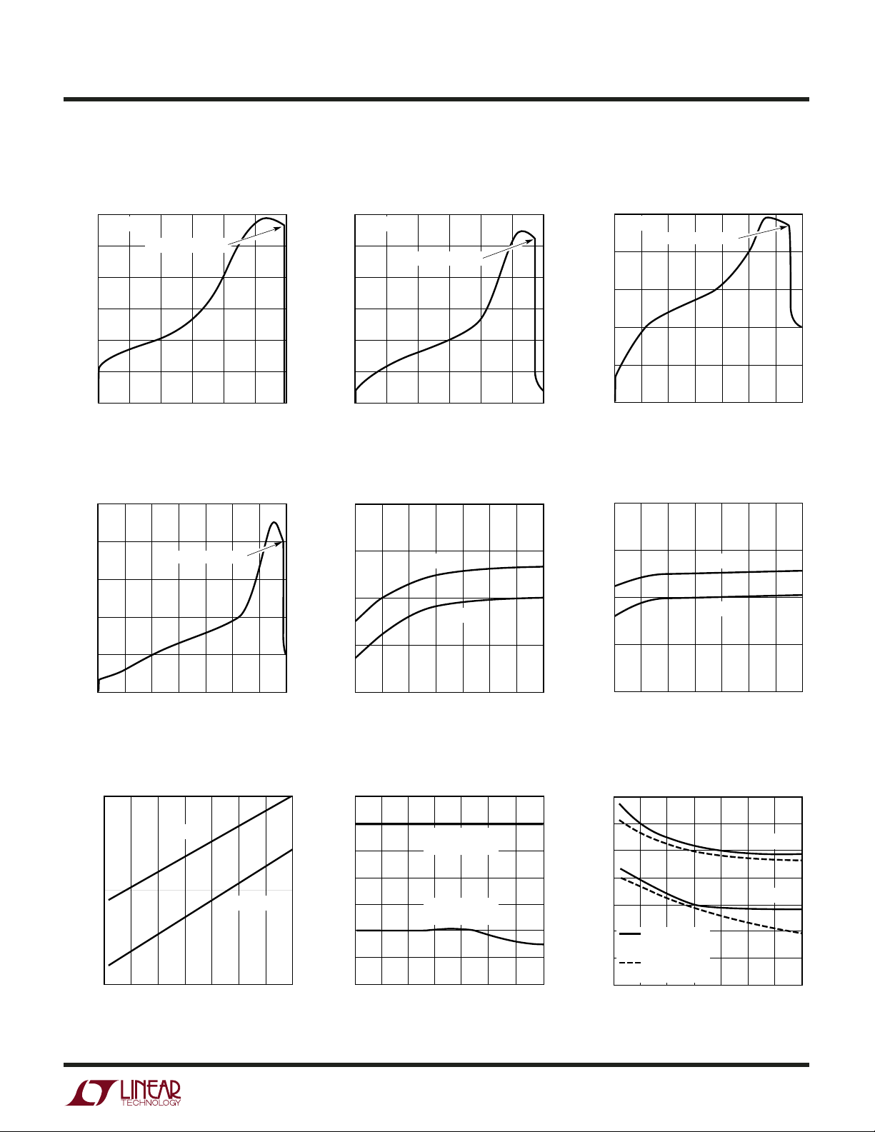
TYPICAL PERFOR A CE CHARACTERISTICS
LTC4060
NiMH Battery Charging
Characteristics at 1C Rate
1.70
TA = 25°C
–∆V TERMINATION
1.65
1.60
CELL VOLTAGE (V)
1.55
0
10 20 30 40
CHARGE TIME (MINUTES)
NiCd Battery Charging
Characteristics at C/2 Rate
1.65
1.60
–∆V TERMINATION
1.55
1.50
CELL VOTLAGE (V)
1.45
NiCd Battery Charging
Characteristics at 1C Rate
1.7
TA = 25°C
–∆V TERMINATION
1.6
1.5
CELL VOLTAGE (V)
1.4
0
50
60
4060 G01
10 20 30 40
CHARGE TIME (MINUTES)
I
vs Temperature and
FCH
50
60
4060 G02
Supply Voltage
2.010
2.005
(A)
2.000
FCH
I
1.995
VCC = 10V
VCC = 4.5V
NiMH Battery Charging
Characteristics at C/2 Rate
1.60
TA = 25°C
1.55
1.50
1.45
CELL VOTLAGE (V)
1.40
1.35
020
I
–∆V TERMINATION
60
40
CHARGE TIME (MINUTES)
vs Temperature and
FCL
Supply Voltage
402
401
(mA)
400
FCL
I
399
80
VCC = 10V
VCC = 4.5V
100
120
140
4060 G03
1.40
–260
(µA)
–300
BRD
I
–340
020
–50
60
40
CHARGE TIME (MINUTES)
I
vs Temperature and
BRD
Supply Voltage
VCC = 10V
–25 0 25 50
TEMPERATURE (°C)
80
100
120
4060 G04
VCC = 4.5V
75 100 125
4060 G07
140
1.990
–50
–25 0 25 50
V
MDV
Supply Voltage
18
16
14
12
(mV)
MDV
10
V
8
6
4
–50
–25 0
TEMPERATURE (°C)
75 100 125
vs Temperature and
NiCd
4.5V ≤ V
4.5V ≤ V
TEMPERATURE (°C)
≤ 10V
CC
NiMH
≤ 10V
CC
50 100 125
25 75
4060 G05
4060 G08
398
–50
–25 0 25 50
t
vs Temperature and
ACC
Supply Voltage
TEMPERATURE (°C)
75 100 125
4060 G06
4060f
5

LTC4060
U
UU
PI FU CTIO S
DRIVE (Pin 1): Base Drive Output for the External PNP
Pass Transistor. Provides a controlled sink current that
drives the base of the PNP. This pin has current limit
protection for the LTC4060.
BAT (Pin 2): Battery Voltage Sense Input Pin. The LTC4060
uses the voltage on this pin to monitor battery voltage and
control the battery current during charging. An internal
resistor divider is connected to this pin which is disconnected when in shutdown or when no power is applied to
VCC.
SENSE (Pin 3): Charge Current Sense Node Input. Current
from V
tor and reappears at the SENSE pin to supply current to the
external PNP emitter. The PNP collector provides charge
current directly to the battery.
TIMER (Pin 4): Charge Timer Input. A capacitor connected
between TIMER and GND along with a resistor connected
from PROG to GND programs the charge cycle timing
limits.
SHDN (Pin 5): Active Low Shutdown Control Logic Input.
When pulled low, charging stops and the LTC4060 supply
current is minimized.
PAUSE (Pin 6): Pause Enable Logic Input. The charger can
be paused, turning off the charge current, disabling termination and stopping the timer when this pin is high. A low
level will resume the charging process.
PROG (Pin 7): Charge Current Programming Input. Provides a virtual reference of 1.5V for an external resistor
(R
PROG
battery charge current. The fast charge current will be 930
times the current through this resistor. This voltage is also
usable as system voltage reference.
passes through the internal current sense resis-
CC
) tied between this pin and GND that programs the
SEL0, SEL1 (Pins 9, 10): Number of Cells Selection Logic
Input. For single cell, connect both pins to GND. For two
cells, connect SEL1 to GND and SEL0 to V
cells, SEL1 connects to V
cells, connect both pins to V
NTC (Pin 11): Battery Temperature Input. An external NTC
thermistor network may be connected to NTC to provide
temperature-based charge qualification. Connecting NTC
to GND inhibits this function.
CHEM (Pin 12): Battery Chemistry Selection Logic Input.
When connected to a high level NiCd fast charge –∆V
termination parameters are used. A low level selects NiMH
parameters.
ACP (Pin 13): Open-Drain Power Supply Status Output.
When V
old, the ACP pin will pull to ground. Otherwise the pin is
high impedance. This output is capable of driving an LED.
VCC (Pin 14): Power Input. This pin can be bypassed to
ground with a capacitance of 1µF.
CHRG (Pin 15): Open-Drain Charge Indicator Status Output. The LTC4060 indicates it is providing charge to the
battery by driving this pin to GND. If charging is paused or
suspended due to abnormal battery temperature, the pin
remains pulled to GND. Otherwise the pin is high impedance. This output can drive an LED.
GND (Pin 16): Ground. This pin provides a ground for the
internal voltage reference and other circuits. All voltage
thresholds are referenced to this pin.
Exposed Pad (Pin 17): Thermal Connection. Internally
connected to GND. Solder to PCB ground for optimum
thermal performance.
is greater than the undervoltage lockout thresh-
CC
and SEL0 to GND. For four
CC
.
CC
For three
CC.
ARCT (Pin 8): Autorecharge Threshold Programming
Input. When the average cell voltage falls below this
threshold, charging is reinitiated. The voltage on this pin
is conveniently derived by using two series PROG pin
resistors and connecting to their common. Connecting
ARCT to VCC invokes a default threshold of 1.3V. Connecting ARCT to GND inhibits autorecharge.
6
4060f

BLOCK DIAGRA
VOLTAGE
REFERENCE
1.5V
PROG
R
PROG
7
NTC
11
CHRG
15
ACP
13
SHDN
5
PAUSE
6
W
I
OSC
+
–
THERMISTOR
I
I/5
A1
INTERFACE
CURRENT
DIVIDER
I I/5
R1
31.5Ω
–
V
CC
COLD
HOT
CUTOFF
CHARGER STATE
CONTROL LOGIC
I
OSC
14
A2
V
CC
+
R2
0.03Ω
SUPPLY GOOD
OUTPUT DRIVER
CURRENT LIMIT
OVERTEMPERATURE
DETECT
AND
IC
UVLO
A/D
CONVERTER
BATTERY
DETECTOR
SEL0
SEL1
SENSE
DRIVE
I
BRD
BAT
LTC4060
3
1
2
+
GND
16, 17
12
CHEM
10
SEL1
SEL0
9
OSCILLATOR
TIMER
4
C
TIMER
AUTORECHARGE
DETECTOR
ARCT
8
4060 BD
4060f
7

LTC4060
OPERATIO
U
The LTC4060 is a complete linear fast charging system for
NiMH or NiCd batteries. Operation can be understood by
referring to the Block Diagram, State Diagram (Figure 1)
and application circuit (Figure 2). While in the unpowered
sleep mode, the battery is disconnected from any internal
loading. The sleep mode is exited and the shutdown mode
is entered when VCC rises above the UVLO (Undervoltage
Lock Out) exit threshold. The UVLO thresholds are dependent upon the number of series cells programmed by the
SEL0 and SEL1 pins. When shutdown occurs the ACP pin
goes from a high to low impedance state. The shutdown
mode is exited and the charge qualification mode entered
SUPPLY
GOOD
LOW OR NO
SUPPLY
SLEEP
(ACP = 0)
when all of the following conditions are met: 1) there is no
manual shutdown command from SHDN, 2) the battery
overvoltage detector does not detect a battery overvoltage, 3) the battery removal detector detects a battery in
place, 4) pause is inactive and 5) the IC’s junction temperature is normal. Once in the charge qualification mode the
thermistor interface monitors an optional thermistor network to determine if the battery temperature is within
charging limits. If the temperature is found within limits
charging can begin. While charging, the CHRG pin pulls to
GND which can drive an LED.
MANUAL
SHUTDOWN
(SHDN = 0)
BATTERY REMOVED,
SHUTDOWN
BATTERY OVERVOLTAGE,
CHARGE PERIOD TIMED
OUT OR IC TOO HOT
< AUTORECHARGE
V
CELL
THRESHOLD
AUTOMATIC
RECHARGE
–∆V TERMINATION
ADEQUATE SUPPLY
AND CHARGER ENABLED
CHARGE
QUALIFICATION
BATTERY PRESENT AND
TEMPERATURE GOOD
(OPTIONAL)
PRECHARGE
/5)
(I
MAX
ADEQUATE V
TEMPERATURE GOOD
(OPTIONAL)
FAST CHARGE
)
(I
MAX
4060 F01
CELL
AND
8
Figure 1. LTC4060 Basic State Diagram
4060f

OPERATIO
LTC4060
U
The charge current is set with an external current programming resistor connected between the PROG pin and
GND. In the Block Diagram, amplifier A1 will cause a virtual
1.5V to appear on the PROG pin and thus, all of the programming resistor’s current will flow through the N-channel
FET to the current divider. The current divider is controlled
by the charger state control logic to produce a voltage
across R1, appropriate either for precharge (I/5) or for fast
charge (I), depending on the cell voltage. The current divider also produces a constant current I
with an external capacitor tied to the TIMER pin, sets the
Oscillator’s clock frequency. During charging, the external
PNP transistor’s collector will provide the battery charge
current. The PNP’s emitter current flows into the SENSE
pin and through the internal current sense resistor R2
(0.03Ω). This current is slightly more than the collector
current since it includes the base current. Amplifier A2 and
the output driver will drive the base of the external PNP
through the DRIVE pin to force the same reference voltage
that appears across R1 to appear across the R2. The precision ratio between R1 and R2, along with the current
programming resistor, accurately determines the charge
current.
When charging begins, the charger state control logic will
enable precharge of the battery. When the cell voltage
exceeds the fast charge qualification threshold, fast charge
begins. If the cell voltage exceeds the initial delay hold off
threshold voltage just prior to precharge, then the A/D
converter immediately monitors for a –∆V event to
terminate charging while in fast charge. Otherwise, the
fast charge voltage stabilization hold off period must
expire before the A/D converter monitors for a –∆V event
from which to terminate charging. The –∆V magnitude for
termination is selected for either NiMH or NiCd by the
CHEM pin. Should the battery temperature become too hot
or too cold, charging will be suspended by the charger
state control logic until the temperature enters normal
limits. A termination timer puts the charger into shutdown
mode if the programmed time has expired. After charging
has ended, the optional autorecharge detector function
monitors for the battery voltage to drop to either a default
or externally programmed cell voltage before automatically restarting a charge cycle.
, that along
OSC
The SHDN pin can be used to return the charger to a
shutdown and reset state. The PAUSE pin can be used to
pause the charge current and internal clocks for any
interval desired.
Fault conditions, such as overheating of the IC due to
excessive PNP base current drive, are monitored and
limited by the IC overtemperature detection and output
driver and current limit blocks.
When either VCC is removed or manual shutdown is
entered, the charger will draw only tiny leakage currents
from the battery, thus maximizing standby time. With V
removed, the external PNP’s base is connected to the
battery by the charger. In manual shutdown, the base is
connected to VCC by the charger.
Undervoltage Lockout
An internal undervoltage lockout circuit (UVLO) monitors
the input voltage and keeps the charger in the inactive
sleep mode until VCC rises above the undervoltage exit
threshold. The ACP pin is high impedance while in the
sleep mode and becomes low impedance to ground when
in the active mode. The threshold is dependent upon the
number of series cells selected by the SEL0 and SEL1 pins
(see V
table). The UVLO circuit has a built-in hysteresis of 100mV.
The thresholds are chosen to provide a minimum voltage
drop of approximately 600mV between minimum V
BAT at a battery cell voltage of 1.8V. This helps to protect
against excessive saturation in the external power PNP
when the supply voltage is near its minimum. While
inactive the LTC4060 reduces battery current to just a
negligible leakage current (I
Manual Shutdown Control
The LTC4060 can be forced into a low quiescent current
shutdown while VCC is present by applying a low level to
the SHDN pin. In manual shutdown, charging is inhibited,
the internal timer is reset and oscillator disabled, CHRG
status output is high impedance and ACP continues to
provide the correct status. The LTC4060 will draw low current from the supply (ISD), and only a negligible leakage
current is applied to the battery (I
UVI1-3
and V
in the Electrical Characteristics
UVD1-3
).
BSL
). If a high level is
BSD
CC
CC
and
4060f
9

LTC4060
OPERATIO
U
applied to the SHDN pin, shutdown ends and charge qualification is entered.
Charge Qualification
After exiting the sleep or shutdown modes the LTC4060
will check for the presence of a battery and for proper
battery temperature (if a thermistor is used) before initiating charging.
When V
a battery is assumed to be present. Should V
above 1.95V (V
CELL
(V
/Number of Cells) is below 2.05V (VBR),
BAT
) for a time greater than the battery
BOV
CELL
rise
overvoltage event delay shown in the far right column of
Table 1, then a battery overvoltage condition is detected
and charging stops. Once stopped in this way, qualification can be reinitiated after V
(V
BOV
– V
) only by removing and replacing the battery
BOVH
has fallen below 1.9V
CELL
(or replacing the battery if the overvoltage condition is a
result of battery removal), toggling the SHDN pin low to
high or removing and reapplying power to the charger.
If the NTC pin voltage is above the temperature disable
threshold (V
), the LTC4060 verifies that the ther-
NDIS
mistor temperature is between 5°C and 45°C. Charging
will not initiate until these temperature limits are met.
The LTC4060 continues to qualify important voltage and
temperature parameters during all charging states. If V
CC
drops below the undervoltage lockout threshold, sleep
mode is entered.
If the internal die temperature becomes excessive, charging stops and the part enters the shutdown state. Once in
the shutdown state charge qualification can be reinitiated
only when the die temperature drops to normal and then
by removing and replacing the battery or toggling the
SHDN pin low to high or removing and reapplying power
to the charger.
Precharge
The state that is entered when qualified charging begins is
precharge. The CHRG status output is set low and remains
low during both precharge and fast charge. If the voltage
on V
is below the 900mV (V
CELL
) fast charge qualifica-
FCQ
tion voltage, the LTC4060 charges using one-fifth the
maximum programmed charge current. The cell voltage is
continuously checked to determine when the battery is
ready to accept a fast charge. Until this voltage reaches
V
, the LTC4060 remains in precharge.
FCQ
If an external thermistor indicates that the sensed temperature is beyond a range of 5°C to 45°C charging is
suspended, the charge timer is paused and the CHRG
status output remains low. Normal charging resumes
from the previous state when the sensed temperature
rises above 5°C or falls below 45°C.
Fast Charge
When the average cell voltage exceeds V
, the LTC4060
FCQ
transitions from the precharge to the fast charge state and
Table 1. LTC4060 Time Limit Programming Examples
TYPICAL BATTERY CHARGE BATTERY AUTOMATIC
FAST VOLTAGE TIME VOLTAGE RECHARGE UVLO EXIT, BATTERY
FAST CHARGE STABILIZATION LIMIT SAMPLING ENTRY INSERTION/REMOVAL/OVERVOLTAGE,
CHARGE RATE HOLD OFF (t
CURRENT R
2A 698Ω 1nF 1.5 4.6 to 5.7 1.1 15 15 to 31 175 to 260
2A 698Ω 1.5nF 1 6.9 to 8.4 1.6 23 23 to 46 260 to 390
2A 698Ω 1.8nF 0.75 8.4 to 10.3 2 28 28 to 56 320 to 480
2A 698Ω 2.7nF 0.5 12.6 to 15.4 3 42 42 to 84 480 to 720
400mA 3480Ω 180pF 1.5 4.2 to 5.2 1 14 14 to 28 160 to 240
400mA 3480Ω 270pF 1 6.3 to 7.7 1.5 21 21 to 42 240 to 360
400mA 3480Ω 390pF 0.75 8.9 to 11 2.1 30 30 to 60 340 to 510
400mA 3480Ω 560pF 0.5 12.6 to 15.4 3 42 42 to 84 480 to 720
PROGCTIMER
(C) (MINUTES) (HOURS) (SECONDS) (SECONDS) THERMISTOR EVENT DELAYS (ms)
) INTERVAL DELAY FAST CHARGE ENTRY AND
MAX
10
4060f

OPERATIO
LTC4060
U
charging begins at the maximum current set by the
exter
nal programming resistor connected between the
PROG pin and GND.
If an external thermistor indicates sensed temperature is
beyond a range of 5°C to 55°C charging is suspended, the
charge timer is paused and the CHRG status output
remains low. Normal charging resumes from the previous
state when the sensed temperature rises above 5°C or falls
below 45°C. Voltage-based termination (–∆V) is then
reset and immediately enabled. If voltage-based termination was imminent when the temperature limits were
exceeded, charge termination will occur.
Charge Termination
Once fast charge begins and after an initial battery voltage
stabilization hold-off period shown in Table 1, voltagebased termination (–∆V) is enabled. This period is used to
prevent falsely terminating on a –∆V event that can occur
almost immediately after initiating charging on some
heavily discharged or stored batteries. However, if V
was measured to be above 1.3V (V
to the precharge cycle, then a mostly charged battery is
assumed and voltage-based termination (–∆V) is enabled
without delay.
An internal 1.5mV resolution A/D converter measures the
cell voltage after each battery voltage sampling interval
indicated in Table 1. The peak cell voltage is stored and
compared to the current cell voltage. When the cell voltage
has dropped by at least V
CHEM pin) from the peak for four consecutive battery
voltage sampling intervals, charging is terminated.
Back-up termination is provided by the charge time limiter,
whose time limit is indicated in Table 1, and by a battery
overvoltage detector. Once terminated by back-up termination, charge qualification can be reinitiated only by removing and replacing the battery or toggling the SHDN pin low
to high or removing and reapplying power to the charger.
Automatic Recharge
Once charging is complete, the optional programmable
automatic recharge state can be entered. This state, if
(magnitude selected by the
MDV
) immediately prior
IDT
CELL
enabled, will automatically restart the charger from the
charge qualification state without user intervention whenever the battery cell voltage drops below a set level. With
the advent of low memory effect NiMH and improved NiCd
cells an automatic recharge feature is practical and eliminates the need for very slow trickle charging.
The CHRG status output is high impedance in the automatic recharge state until charging begins. If the V
voltage drops below the voltage set on the ARCT pin for at
least the automatic recharge entry delay time as shown in
Table 1, the charge qualification state is entered and
charging will begin anew in fast charge. An easy way of
setting the voltage on the ARCT pin is by using two series
current programming resistors and connecting their common to the ARCT pin as shown in Figure 2. The PROG pin
will provide a constant 1.5V (V
voltage range of the ARCT pin is approximately 0.8V to
1.6V. A preprogrammed recharge threshold of 1.3V (V
is selected when the ARCT pin is connected to V
(V
pin is connected to ground (V
Pause
After charging is initiated, the PAUSE pin may be used to
pause operation at any time. Whenever the voltage on the
PAUSE pin is a logic high, the charge timer and all other
timers pause, charging is stopped and the fast charge termination algorithm is inhibited. The CHRG status output
remains at GND. If voltage-based termination was imminent before pause, charge termination will occur. Otherwise,
when pause ends, the charge timer and all other timers
resume timing, charging restarts and voltage-based termination (–∆V) is reset and immediately enabled. If the battery is removed while the PAUSE pin is a logic high, then
battery removal is detected and shutdown is entered. If the
battery is replaced while the PAUSE pin is a logic high, it
will not be detected until pause is turned off.
For pause periods or a series of periods where the battery
capacity could be significantly depleted, consider using
shutdown instead of pause to avoid having the safety timer
expire before the battery can be fully charged. Shutdown
resets the safety timer.
). Automatic recharge is disabled when the ARCT
ARDEF
). The programmable
PROG
).
ARDIS
CELL
ARDT
)
CC
4060f
11

LTC4060
OPERATIO
U
Battery Chemistry Selection
The desired battery chemistry is selected by programming
the CHEM pin to the proper voltage. When wired to GND,
a set of parameters specific to charging NiMH cells is
selected. When CHEM is connected to VCC, charging is
optimized for NiCd cells. The various charging parameters
are detailed in Table 2.
Cell Selection
The number of series cells is selected using the SEL0 and
SEL1 pins. For one cell, both pins connect to GND. For two
cells, SEL0 connects to VCC and SEL1 to GND. For three
cells, SEL0 connects to GND and SEL1 to VCC. For four
cells, both connect to VCC.
Table 2. LTC4060 Charging Parameters
STATE CHEM CHARGE TIME LIMIT T
Precharge Both t
Fast Charge NiCd t
NiMH t
MAX
MAX
MAX
MIN
5°C45°CI
5°C55°CI
5°C55°CI
T
MAX
Insertion and Removal of Batteries
The LTC4060 automatically senses the insertion or removal of a battery by monitoring the V
pin voltage.
CELL
Either the charge current, or if not charging then an
internal pull-up current (I
), will pull V
BRD
up when the
CELL
battery is removed. When this voltage rises above 2.05V
(VBR) for a time greater than the battery removal event
delay shown in Table 1, the LTC4060 considers the battery
to be absent. Inserting a battery, causing V
below both VBR and 1.95V (V
) for a period longer than
BOV
CELL
to fall
the battery insertion event delay shown in Table 1, results
in the LTC4060 recognizing a battery present and initiates
a completely new charge cycle beginning with charge
qualification. All battery currents are inhibited while in
shutdown.
I
CHRG
MAX
MAX
MAX
TYPICAL TERMINATION CONDITION
/5 V
≥ 0.9V
CELL
–16mV Per Cell After Initial t
–8mV Per Cell After Initial t
MAX
MAX
/12 Delay
/12 Delay
WUUU
APPLICATIO S I FOR ATIO
Programming Charge Current
The battery charge current is set with an external program
resistor connected from the PROG pin to GND. The formula for the battery fast charge current or I
II
=
MAX PROG
()
•
⎜
⎝
R
⎛
=
.
15
PROG
⎞
V
•930
930
⎟
⎠
or
R
PROG
where R
1395
=
I
MAX
is the total resistance from the PROG pin to
PROG
ground. For example, if 1A of fast charge current is
required:
R
PROG
1395
==
A
1
k
14. 1% Resistor
MAX
is:
Under precharge conditions, the current is reduced to
20% of the fast charge value (I
).The LTC4060 is
MAX
designed for a maximum current of 2A. This translates to
a maximum PROG pin current of 2.15mA and a minimum
program resistor of 698Ω. Reduced accuracy at low
current limits the useful fast charge current to a minimum
of approximately 200mA. Errors in the charge current can
be statistically approximated as follows:
One Sigma Error ≅ 7mA
For best stability over temperature and time, 1% metalfilm resistors are recommended. Capacitance on the PROG
pin should be limited to about 75pF to insure adequate AC
phase margin for its amplifier.
Different charge currents can be programmed by various
means such as by switching in different program resistors. A voltage DAC connected through a resistor to the
PROG pin or a current DAC connected in parallel with a
12
4060f

WUUU
APPLICATIO S I FOR ATIO
LTC4060
resistor to the PROG pin can also be used to program
current. Note that this will alter the timer periods unless
alternate TIMER pin capacitors are also programmed
through an analog switch.
The PROG pin provides a reference voltage of 1.5V (V
PROG
)
that may be tapped for system use. Current loading on
PROG is multiplied by 930 and appears as increased I
This may be compensated by adjustment of R
PROG
MAX.
. Total
PROG pin current must be limited to 2.3mA otherwise
absolute maximum ratings will be exceeded. When the
LTC4060 is in the shutdown mode, the PROG pin is forced
to ground potential to save power.
Programming the Timer
All LTC4060 internal timing is derived from the internal
oscillator that is programmed with an external capacitor at
the TIMER pin. The time periods shown in Table 1 scale
directly with the timer period. The programmable safety
timer is used to put a time limit on the entire charge cycle
for the case when charging has not otherwise terminated.
The time limit is programmed by an external capacitor at
the TIMER pin and is also dependent on the current set by
the programming resistor connected to the PROG pin. The
time limit is determined by the following equation:
t
(Hours) = 1.567 • 106 • R
MAX
CF
TIMER
()
=
.• • ()
t Hours
()
MAX
6
R
PROG
PROG
(Ω) • C
Ω1 567 10
TIMER
(F)
Some typical timing values are detailed in Table 1. The
timer begins at the start of a charge cycle. After the timeout occurs, the charge current stops and the CHRG output
assumes a high impedance state to indicate that the
charging has stopped.
Excessively short time-out periods may not allow enough
time for the battery to receive full charge or may result in
premature –∆V termination due to too short a battery
voltage stabilization hold-off period. Excessively long timeout periods may indicate too low a charge current which
may not allow voltage-based termination (–∆V) to work
properly. Time-out limits of less than 0.75 hour for faster
2C charge rates, or more than 3.5 hours for slower C/2
charge rates, are generally not recommended. Consult the
battery manufacturer for recommended periods.
An external timing source can also be used to drive the
TIMER pin for precise or programmed control. The high
level must be between 2.5V and V
and the low level must
CC
be between 0V and 0.25V. Also, the driving source must be
able to overdrive the internal current source and sink
which is 5% of the current through R
PROG
.
Battery Temperature Sensing
Temperature sensing is optional in LTC4060 applications.
To disable temperature qualification of all charging operations, the NTC pin must be wired to ground. A circuit for
temperature sensing using a thermistor with a negative
temperature coefficient (NTC) is shown in Figure 2. Internally derived VCC proportional voltages (V
CLD
, V
HTI
, V
HTC
)
are compared to the voltage on the NTC input pin to test the
temperature thresholds. The battery temperature is measured by placing the thermistor close to the battery pack.
In Figure 2, a common 10k NTC thermistor such as a
Murata NTH4G series NTH4G39A103F can be used. R
HOT
should be a 1% resistor with a value equal to the value of
the chosen NTC thermistor at 45°C (V
NTC
= V
= 0.5 • V
HTI
CC
typ). Another temperature may be chosen to suit the
battery requirements. The LTC4060 will not initiate a
charge cycle or continue with a precharge if the value of the
thermistor falls below 4.42k which is a temperature rising
to approximately 45°C. However, once fast charging is in
progress, it will not be stopped until the thermistor drops
below 3k which is a temperature rising to approximately
55°C (V
NTC
= V
= 0.4 • VCC typ). Once reaching this
HTC
charge cutoff threshold, charging is suspended until the
value of the thermistor rises above approximately 4.8k
(falling temperature) or approximately 43°C (45°C – 2°C
hysteresis at V
= 5V) and then charging is resumed.
CC
Hysteresis avoids possible oscillation about the trip points.
Note that the comparator hysteresis voltages are constant
and when VCC increases the signal level from the thermistor increases thus making the temperature hysteresis
look smaller.
During suspension the charge current is turned off and the
safety timer is frozen. The LTC4060 is also designed to
suspend when the thermistor rises above 34k (falling
4060f
13

LTC4060
WUUU
APPLICATIO S I FOR ATIO
temperature) at approximately 0°C (5°C – 5°C hysteresis
at V
below 27k (rising temperature) which will be approximately 5°C (V
Many thermistors with an R
mately 7 will work. For lower power dissipation higher
values of thermistor resistance can be used. The Murata
NTH4G series offers resistances of up to 100k at 25°C.
It is important that the thermistor be placed in close
contact with the battery and away from the external PNP
pass transistor to avoid excessive temperature errors on
the sensed battery temperature. Furthermore, since VCC is
a high current path into the LTC4060, it is essential to
minimize voltage drops between the VCC supply pin and
the top of R
VCC pin.
Power Requirements
The DC power input to the VCC pin must always be within
proper limits while charging a battery. Voltages beyond
the absolute maximum ratings may damage the charger
and voltages falling below the UVLO entry thresholds, as
programmed by the SEL0 and SEL1 pins, will likely cause
the charger to enter the shutdown state (when the UVLO
exit threshold is exceeded charging will begin anew). While
the LTC4060 is designed to reject 60Hz or 120Hz supply
ripple, certain precautions are required. The instantaneous
ripple voltage must always be within the above mentioned
limits. Ripple voltage seen across the collector-base junction of the external PNP pass transistor will slightly modulate its beta and hence its base current. Since the emitter
current is precisely regulated by the LTC4060, any modulation of base current will appear at the collector. This
slightly modulated battery charge current into a battery
will usually produce an insignificant modulation voltage at
the battery. However, if excessive wire impedance to the
battery from the PNP exists, then it may be helpful to Kelvin
connect the BAT pin to a convenient point closest to the
battery to reduce ripple magnitude entering the LTC4060’s
battery monitoring circuits. The battery ground impedance should also be managed to limit ripple voltage at the
BAT pin. Excessive ripple into the BAT pin may cause the
charger to deviate from specified performance.
= 5V) and then resume when the thermistor falls
CC
= V
NTC
by Kelvin connecting R
HOT
= 0.86 • VCC typ).
CLD
to R
COLD
ratio of approxi-
HOT
directly to the
HOT
VCC Bypass Capacitor
A 1µF capacitor located close to the LTC4060 will usually
provide adequate input bypassing. However, caution must
be exercised when using multilayer ceramic capacitors.
Because of the self-resonance and high Q characteristics
of some types of ceramic capacitors, along with wiring
inductance, high voltage transients can be generated
under some conditions such as connecting or disconnecting a supply input to a hot power source. To reduce the Q
and prevent these transients from exceeding the absolute
maximum voltage rating, consider adding about 1Ω of
resistance in series with the ceramic input capacitor.
BAT Bypass Capacitor
This optional capacitor, connected between BAT and GND,
can be used to help filter excessive contact bounce during
the battery monitoring or charging process. The value will
depend upon the contact bounce open duration, but is typically 10µF. Another purpose of this capacitor is to bypass
transient battery load events that might otherwise disrupt
monitoring or charging. Should the battery connections not
be subject to excessive contact bounce or excessive battery voltage transients, then no BAT pin capacitor is required. The same caution mentioned above for the VCC bypass capacitor applies.
External PNP Transistor
The external PNP pass transistor must have adequate beta
and breakdown voltages, low saturation voltage and sufficient power dissipation capability that may include heat
sinking.
To provide 2A of charge current with the minimum available base current drive of 40mA (I
minimum PNP beta of 50.
The transistor’s collector to emitter breakdown voltage
must be high enough to withstand the difference between
the maximum supply voltage and minimum battery voltage. Almost any transistor will meet this requirement.
Additionally, when no power is supplied to the charger
(V
= 0V and V
IN
breakdown voltage must be high enough to prevent a
leakage path at the maximum battery voltage while not
= 0V), the transistor’s emitter to base
SENSE
min) requires a
DRV
14
4060f

WUUU
APPLICATIO S I FOR ATIO
LTC4060
charging (the DRIVE pin is internally switched to the BAT
pin). Most transistors will meet this requirement as well.
With low supply voltages, the PNP saturation voltage
(V
) becomes important. The V
CESAT
CESAT
must be less
than the minimum supply voltage minus the maximum
voltage drop across the internal current sense resistor and
bond wires (approximately 0.08Ω) and maximum battery
voltage presented to the charger accounting for wire I • R
drops.
V
CESAT
(V) < V
DD(MIN)
– (I
BAT(MAX)
• 0.08Ω + V
BAT(MAX)
)
For example, if it were desired to have a programmed
charge current of 2A with a minimum supply voltage of
4.75V and a maximum battery voltage of 3.6V (2 series
cells at 1.8V each), then the minimum operating V
V
(V) = 4.75 – (2 • 0.08 + 3.6) = 0.99V
CESAT
CESAT
is:
If the PNP transistor cannot achieve the saturation voltage
required, base current will dramatically increase. This is to
be avoided for a number of reasons: DRIVE pin current
may reach current limit resulting in the LTC4060 characteristics going out of specifications, excessive power
dissipation may force the IC into thermal shutdown, or the
battery could discharge because some of the current from
the DRIVE pin could be pulled from the battery through the
forward biased PNP collector base junction.
The actual battery fast charge current (I
) is slightly less
BAT
than the regulated charge current because the charger
senses the emitter current and the battery charge current
will be reduced by the base current. In terms of β (IC/IB)
I
can be calculated as follows:
BAT
⎛
⎞
IA I
() •=
BAT PROG
If β = 100 then I
930
is 1% low. The 1% loss can be easily
BAT
compensated for by increasing I
β
⎜
⎟
+
1
β
⎝
⎠
by 1%.
PROG
Another important factor to consider when choosing the
PNP pass transistor is its power handling capability. The
transistor’s data sheet will usually give the maximum rated
power dissipation at a given ambient temperature with a
power derating for elevated temperature operation. The
maximum power dissipation of the PNP when charging is:
P
D(MAX)
V
DD(MAX)
(W) = I
MAX(VDD(MAX)
is the maximum supply voltage and V
– V
BAT(MIN)
)
BAT(MIN)
is
the minimum battery voltage when discharged, but not
less than 0.9V/cell since less than 0.9V/cell invokes
precharge current levels.
Thermal Considerations
Internal overtemperature protection is provided to prevent
excessive LTC4060 die temperature during a fault condition. If the internal die temperature exceeds approximately
145°C, charging stops and the part enters the shutdown
state. The faults can be generated from insuffient heat
sinking, a shorted DRIVE pin or from excessive DRIVE pin
current to the base of an external PNP transistor if it’s in
deep saturation from a very low VCE. Once in the shutdown
state, charge qualification can be reinitiated only by removing and replacing the battery or toggling the SHDN pin
low to high or removing and reapplying power to the
charger. This protection is not designed to prevent overheating of the PNP pass transistor. Indirectly though, selfheating of the PNP thermally conducting to the LTC4060
can result in the IC’s junction temperature rising above
145°C, thus cutting off the PNP’s base current. This action
will limit the PNP’s junction temperature to some temperature well above 145°C. The user should insure that the
maximum rated junction temperature is not exceeded
under any normal operating condition. See Package/Order
Information for the θJA of the LTC4060 Exposed Pad
packages. The actual thermal resistance in the application
will vary depending on forced air cooling, use of the
Exposed Pad and other heat sinking means, especially the
amount of copper on the PCB to which the LTC4060 is
attached. The majority of the power dissipated within the
LTC4060 is in the current sense resitor and DRIVE pin
driver as given below:
PD = (I
TJ = TA + θJA • P
)2 • 0.08 + I
BAT
(VCC – VEB)
DRIVE
D
VEB is the emitter to base voltage of the external PNP.
4060f
15

LTC4060
TYPICAL APPLICATIO S
U
Full Featured 2A Charger Application
Figure 2 shows an application that utilizes the optional
temperature sensing and optional externally programmable automatic recharge features. It also has LEDs to
indicate charging status and the presence of sufficient
input supply voltage.
The PROG pin has a total resistance of 691Ω to ground
that programs the fast-charge current at the PNP’s emitter
to 2.02A (2A at the collector for beta of 100). The ARCT pin
voltage is programmed to 1.25V. When the battery cell
voltage falls below this automatic recharge will begin.
Optional capacitor C
filters excessive contact bounce.
BAT
This circuit can be modified to charge a 4A-Hr battery at a
C/2 rate simply by doubling the C
R
4.42k
“CHARGE”
TIMER
HOT
R
NTC
10k
capacitance.
R
LED
330Ω
5
SHDN
15
CHRG
11
NTC
7
PROG
R
PROG
115Ω
R
ARCT
576Ω
8
ARCT
9
SEL0
10
SEL1
V
5V
IN =
14
V
CC
SENSE
DRIVE
LTC4060
TIMER
PAUSE
GND
16
ACP
BAT
CHEM
Power Path Control
Proper power path control is an important consideration
when fast charging nickel cells. This control ensures the
system load remains powered at all times, but that normal
system operation and associated load transients do not
adversely affect the charging procedure. Figure 3 illustrates a 1A charger with power path control. When VIN is
applied the forward biased Schottky diode will power the
load while the P-channel FET will disconnect the battery
from the load. When VIN is removed, the FET will turn-on
to provide a low loss switch from the battery to the load,
and the diode will isolate V
presense of V
R
LED
330Ω
MJD210
4060 F02
“AC”
C
TIMER
1.5nF
13
3
1
2
4
12
6
IN
.
C
BAT
10µF
+
. The ACP output signals the
IN
2-CELL
NiMH
BATTERY
16
R
330Ω
“CHARGE”
R
PROG
1400Ω
Figure 2. Full Featured 2A Charger Application
V
5V
IN =
LED
V
SHDN
CHRG
NTC
PROG
ARCT
SEL0
SEL1
CC
ACP
SENSE
DRIVE
LTC4060
BAT
TIMER
CHEM
PAUSE
GND
16
5
15
11
7
8
9
10
R
AC
10k
13
3
1
2
4
12
6
FZT948
ACP
C
TIMER
820pF
+
2-CELL
NiMH
BATTERY
*DRAIN SOURCE DIODE OF MOSFET
Figure 3. 1A Charger Application with Power Path Control
B220A
FDG312P
*
C
10µF
4060 F03
TO LOAD
LOAD
4060f

TYPICAL APPLICATIO S
LTC4060
U
Trickle Charge
The trickle charge function is normally not required due to
the automatic recharge feature. However, the LTC4060
does provide a modest pull-up current (I
) as part of its
BRD
battery removal detection method. If additional current is
required for trickle charge or to support battery removal
detection with current loads greater than I
, then the
BRD
simple circuit of Figure 4 will facilitate that. The diode
insures no reverse discharge current when V
is removed
IN
and the resistor sets the trickle current.
Extending Charge Current
Extending the charge current beyond 2A can be accomplished by paralleling an external current sense resistor,
R
with the internal current sense resistor as shown in
ISET,
Figure 5. Bond wire, lead frame and PCB interconnect
V
IN
14
V
CC
LTC4060
SENSE
DRIVE
BAT
3
1
2
resistance and mismatches in the two sense resistor’s
value will cause charge current variability to increase in
proportion to the extension in current. Resistor R
ISET
should be connected directly to the LTC4060 to reduce
errors. The total current sense resistor, bond wire and lead
frame resistance is approximately 0.08Ω (T.C. ≅ 3500ppm/
°C). The formula for extended fast charge current is:
II
MAX EXT MAX
for R
ISET
=+
()
AA
•.
==
2153
= 0.16Ω and R
⎛
•
1
⎜
⎝
PROG
.
008
R
ISET
= 698Ω.
⎞
⎟
⎠
Adequate PNP beta is required to meet the DRIVE pin
capability and the increased PNP power dissipation will
require additional heat sinking.
1N4001
3.3k
+
2-CELL
NiMH
BATTERY
4060 F04
Figure 4. Adding Trickle Charge
V
IN
14
V
CC
0.08Ω
SENSE
DRIVE
LTC4060
Figure 5. Extended Charge Current Operation
BAT
R
ISET
0.16Ω
3
1
2
+
2-CELL
NiMH
BATTERY
4060 F05
4060f
17

LTC4060
TYPICAL APPLICATIO S
U
Reverse Input Voltage Protection
In some applications protection from reverse supply voltage is desired. If the supply voltage is high enough, a
series blocking diode can be used. In other cases, where
the voltage drop must be kept very low, a P-channel FET
as shown in Figure 6 can be used.
*
LTC4060
V
IN
*DRAIN BULK DIODE OF MOSFET
Figure 6. Low Loss Reverse Input Voltage Protection
14
V
CC
4060 F06
18
4060f

PACKAGE DESCRIPTIO
LTC4060
U
DHC Package
16-Lead Plastic DFN (5mm × 3mm)
(Reference LTC DWG # 05-08-1706)
0.65 ±0.05
3.50 ±0.05
1.65 ±0.05
(2 SIDES)2.20 ±0.05
4.40 ±0.05
(2 SIDES)
RECOMMENDED SOLDER PAD PITCH AND DIMENSIONS
5.00 ±0.10
(2 SIDES)
PIN 1
TOP MARK
(SEE NOTE 6)
0.200 REF
NOTE:
1. DRAWING PROPOSED TO BE MADE VARIATION OF VERSION (WJED-1) IN JEDEC
PACKAGE OUTLINE MO-229
2. DRAWING NOT TO SCALE
3. ALL DIMENSIONS ARE IN MILLIMETERS
4. DIMENSIONS OF EXPOSED PAD ON BOTTOM OF PACKAGE DO NOT INCLUDE
MOLD FLASH. MOLD FLASH, IF PRESENT, SHALL NOT EXCEED 0.15mm ON ANY SIDE
5. EXPOSED PAD SHALL BE SOLDER PLATED
6. SHADED AREA IS ONLY A REFERENCE FOR PIN 1 LOCATION ON THE
TOP AND BOTTOM OF PACKAGE
0.25 ± 0.05
0.50 BSC
PACKAGE
OUTLINE
3.00 ±0.10
(2 SIDES)
0.75 ±0.05
R = 0.20
1.65 ± 0.10
(2 SIDES)
0.00 – 0.05
TYP
R = 0.115
TYP
0.25 ± 0.05
0.50 BSC
4.40 ±0.10
(2 SIDES)
BOTTOM VIEW—EXPOSED PAD
169
18
0.40 ± 0.10
PIN 1
NOTCH
(DHC16) DFN 1103
Information furnished by Linear Technology Corporation is believed to be accurate and reliable.
However, no responsibility is assumed for its use. Linear Technology Corporation makes no representation that the interconnection of its circuits as described herein will not infringe on existing patent rights.
4060f
19

LTC4060
PACKAGE DESCRIPTIO
U
FE Package
16-Lead Plastic TSSOP (4.4mm)
(Reference LTC DWG # 05-08-1663)
Exposed Pad Variation BC
3.58
(.141)
4.90 – 5.10*
(.193 – .201)
3.58
(.141)
16 1514 13 12 11
10 9
6.60 ±0.10
4.50 ±0.10
RECOMMENDED SOLDER PAD LAYOUT
0.09 – 0.20
(.0035 – .0079)
NOTE:
1. CONTROLLING DIMENSION: MILLIMETERS
2. DIMENSIONS ARE IN
3. DRAWING NOT TO SCALE
SEE NOTE 4
0.65 BSC
4.30 – 4.50*
(.169 – .177)
0.50 – 0.75
(.020 – .030)
MILLIMETERS
(INCHES)
2.94
(.116)
0.45 ±0.05
1.05 ±0.10
1345678
2
0.25
REF
0° – 8°
0.65
(.0256)
BSC
0.195 – 0.30
(.0077 – .0118)
TYP
4. RECOMMENDED MINIMUM PCB METAL SIZE
FOR EXPOSED PAD ATTACHMENT
*DIMENSIONS DO NOT INCLUDE MOLD FLASH. MOLD FLASH
SHALL NOT EXCEED 0.150mm (.006") PER SIDE
2.94
(.116)
1.10
(.0433)
MAX
0.05 – 0.15
(.002 – .006)
FE16 (BC) TSSOP 0204
6.40
(.252)
BSC
RELATED PARTS
PART NUMBER DESCRIPTION COMMENTS
LTC1732 Lithium-Ion Linear Battery Charger Controller Simple Charger uses External FET, Features Preset Voltages, C/10
LTC1733 Monolithic Lithium-Ion Linear Battery Charger Standalone Charger with Programmable Timer, Up to 1.5A Charge Current
LTC1734 Lithium-Ion Linear Battery Charger in ThinSOTTMSimple ThinSOT Charger, No Blocking Diode, No Sense Resistor Needed
LTC1734L Lithium-Ion Linear Battery Charger in ThinSOT Low Current Version of LTC1734; 50mA ≤ I
LTC1998 Lithium-Ion Low Battery Detector 1% Accurate 2.5µA Quiescent Current, SOT-23
LTC4006/LTC4007 4A Multicell Li-Ion Battery Chargers Standalone Charger, 6V ≤ VIN ≤ 28V, Up to 96% Efficiency,
LTC4008 4A Multichemistry Battery Charger Synchronous Operation for High Efficiency, AC Adapter Current Limit
LTC4052 Monolithic Lithium-Ion Battery Pulse Charger No Blocking Diode or External Power FET Required, ≤1.5A Charge Current
LTC4053 USB Compatible Monolithic Li-Ion Battery Charger Standalone Charger with Programmable Timer, Up to 1.25A Charge Current
LTC4054 Standalone Linear Li-Ion Battery Charger Thermal Regulation Prevents Overheating, C/10 Termination,
in ThinSOT C/10 Indicator, Up to 800mA Charge Current
LTC4055 USB Power Controller and Li-Ion Battery Charger Charges Directly from USB or Wall Adapter, New Topology Charges Faster and
LTC4058 Standalone Li-Ion Linear Charger in DFN Up to 950mA Charge Current, Kelvin Sense for High Accuracy,
LTC4058X C/10 Charge Termination
LTC4411 Low Loss PowerPathTM Controller in ThinSOT Automatic Switching Between DC Sources, Load Sharing,
LTC4412 Replaces ORing Diodes
ThinSOT and PowerPath are trademarks of Linear Technology Corporation.
Linear Technology Corporation
20
1630 McCarthy Blvd., Milpitas, CA 95035-7417
(408) 432-1900 ● FAX: (408) 434-0507
●
www.linear.com
Charger Detection and Programmable Timer, Input Power Good Indication
≤ 180mA
CHRG
±0.8% Charging Voltage Accuracy
More Efficiently
4060f
LT/TP 0904 1K • PRINTED IN THE USA
© LINEAR TECHNOLOGY CORPORATION 2004
 Loading...