


L DESIGN FEATURES
Feature-Packed Charger Handles
All Battery Chemistries and Produces
3A/50W for Fast Charging from a
4mm × 4mm QFN
Introduction
The LTC 4009, L TC400 9 -1 and
LTC4009-2 are a family of high power
battery charger ICs that achieve a small
circuit size and high performance without compromising functionality. The
family operates with high efficiency
while packing the most desirable
charging and protection features into
a space-efficient 20-lead 4mm × 4mm
QFN package. When combined with
just a few external components and
termination control, the LTC4009
family facilitates construction of
chargers capable of delivering up to
3A to batteries with output power
levels approaching 50W. These ICs are
Feature LTC4009 LTC4009-1 LTC4009-2 LTC4008
Output Voltage Selection
especially well-suited to implementing
microprocessor-controlled chargers
for all chemistry types, including
smart batteries.
High Performance
The LTC4009 family builds upon the
proven quasi-constant frequency,
constant off-time PWM control architecture found in other Linear
Technology battery chargers such as
the LTC4006, LTC4007, LTC4008,
and LTC4011. This buck topology
provides continuous switching with
synchronous rectification, even with
no load current.
Table 1. LTC4009 family features
External Resistor
Divider
Pin Programmable
at 4.1V/cell
by James A. McKenzie
Normally the charger operates over
a wide duty cycle range in a manner
similar to a fixed-frequency PWM controller running at 550kHz. However,
if the input or output voltage drives
the duty cycle to extremes, below 20%
or above 80%, the LTC4009 smoothly
adjusts the operating frequency
downward to avoid pulse-skipping
that might otherwise begin to occur
at 550kHz. Under very low dropout
conditions requiring high duty cycle
operation, the internal watchdog
timer on the LTC4009 prevents the
charger from switching below 25kHz.
This allows the charger to achieve a
Pin Programmable
at 4.2V/cell
External Resistor
Divider
Output Voltage Accuracy
(Room Temperature)
Maximum Charge Current 3A 3A 3A 4A
Charge Current Accuracy ±5% ±5% ±5% ±5%
Input Current Limit Accuracy ±4% ±4% ±4% ±7%
Input Current Limit/Indicator
External PWM Switching MOSFETs All NFET All NFET All NFET PFET/NFET
Nominal PWM Frequency 550kHz 550kHz 550kHz 300kHz
Shutdown Pin
C/10 Indicator
Charge Current Monitor
Termination Method External External External External
Fault Indicator
Thermistor Interface
INFET Control
18
±0.5% + Divider Error ±0.6% ±0.6% ±0.8% + Divider Error
L L L L
L L L
L L L L
L L L L
Linear Technology Magazine • September 2008
Merged with ACP
L
L
L
DESIGN FEATURES L
CLP
FROM
ADAPTER
15V AT 2A
BULK
CHARGE
0.1µF
5.1k
D2
D1
D3
Q1
294k
10pF
25mΩ
3.01k
0.1µF
2µF
Q2
Q3
D4
L1
6.8µH
33mΩ
3-CELL
Li-Ion
BATTERY
STACK
DCIN
CHRG
0.1µF
22.1k
2.43k
3k
RED
6.04k
26.7k
53.6k
LTC4009
DCDIV
ACP
ICL
SHDN
ITH
PROG
CLN
BOOST
TGATE
SW
INTV
DD
BGATE
TO/FROM
MCU
GND
CSP
CSN
BAT
FBDIV
V
FB
20µF
POWER TO SYSTEM
0.1µF
4.7nF
20µF
3.01k
31.2k
D2, D4, D5: MBR230LSFT1
D3:CMDSH-3
Q1: 2N7002
Q2, Q3: Si7212DN
L1: IHLP-2525CZ-11
+
D5
maximum duty cycle of 98% or higher
without producing frequencies that
could extend down into the audible
range.
With a synchronous rectifier, not
only are high current applications
supported at efficiency levels greater
than 90%, but switching activity is
continuous and independent of the
load current. Maintaining full continuous conduction mode in the inductor
at final output voltage, under no-load
conditions, avoids pulse-skipping
which can generate audible noise and
provide poor load regulation.
The input current limit accuracy
is typically ±3% and a maximum of
±4% over the full operating temperature range. Output voltage accuracy
is typically ±0.5% and a maximum of
±0.8% over temperature.
Small PCB Footprint
Besides its small surface mount package size, the LTC4009 family offers
other features that drive down the
total solution size.
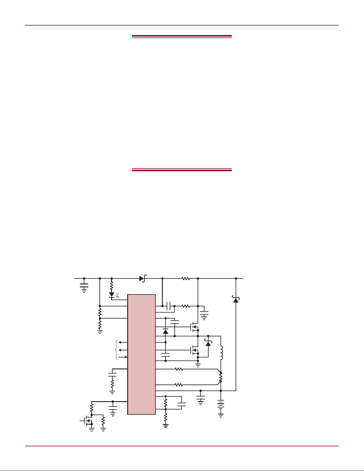
For instance, as shown in Figure 1,
the family supports direct drive of both
an N-channel MOSFET power switch
and N-channel MOSFET synchronous
When combined with just
a few external components
and termination control, the
LTC4009 family facilitates
construction of chargers
capable of delivering
up to 3A to batteries
with output power levels
approaching 50W. These
ICs are especially well
suited to implementing
microprocessor-controlled
chargers for all chemistry
types, including smart
batteries.
rectifier. N-channel MOSFETs are
desirable in high current applications because of their lower R
and the LTC4009 family uses a novel
adaptive gate drive that is insensitive
to MOSFET inertial delays to avoid
overlap conduction losses. Many
suppliers now source dual N-channel
MOSFETs in a single space-efficient
package, often with individual drive
DS(ON)
,
capabilities tailored to synchronous
buck PWM switching topologies.
Increasing the switching frequency
to 550kHz and adjusting internal bias
circuits to allow higher charge current
ripple minimize both the inductor size
and output capacitance requirements.
This is particularly important because
these components tend to dominate
the overall solution size due to continual improvements in IC and passive
SMD packaging technology.
The physical layout of a typical
3A application is shown in Figure 3,
requiring only 240mm2 of board
space.
A Rich Tradition
The LTC4009 family builds upon the
general purpose features offered by
the LTC4008 and the output voltage
programming convenience afforded
by the LTC4006. Each member of the
LTC4009 family contains the same
charge current and input current limit
programming features, along with a
full complement of charge monitoring, safety and fault management
functions. The LTC4009 has a fully
adjustable output voltage, which is set
with a simple resistor divider. Charge
Linear Technology Magazine • September 2008
Figure 1. A 12.6V, 3A lithium-ion charger
19

CLP
18V AT 3A FROM
ADAPTER
CHARGE
CURRENT
MONITOR
0.1µF
5.1k
33mΩ
3.01k
0.1µF
L1
6.8µH
50mΩ
DCIN
0.1µF
2µF
0.1µF
22.1k
1.74k
6.04k
26.7k
LTC4009-1
DCDIV
CHRG
ACP
ICL
SHDN
ITH
PROG
CLN
BOOST
TGATE
SW
INTV
DD
INTV
DD
BGATE
TO/FROM
MCU
GND
CSP
CSN
BAT
FVS1
FVS0
20µF
POWER TO
SYSTEM
4.7nF
20µF
4-CELL
Li-Ion
BATTERY
STACK
3.01k
+
D3
D4
D1
D2
Q2
Q3
D1, D3, D4: MBR230LSFT1
D2: CMDSH-3
Q1, Q2: Si7212DN
L1: IHLP-2525CZ-11
L DESIGN FEATURES
current accuracy is maintained at
output voltages below 6V, making the
LTC4009 ideal for charging nickelbased chemistries or supercaps.
The LTC4009-1 and LTC4009-2
are easy to use in lithium-based
battery products containing one to
four series cells. Each has a range
of output voltages that can be selected simply by strapping two pins
to either ground or the output of the
onboard 5V regulator, as shown for the
LTC4009-1 in Figure 2. No other external components are required to set
this precision voltage. The LTC4009-1
provides 4.1V/cell settings in support
of evolving consumer product safety
standards or coke-anode cells, while
the LTC4009-2 utilizes 4.2V/cell for
conventional full-capacity charging
of graphite-anode lithium-ion packs.
The ICs contain a dedicated PMOS
switch that during shutdown removes
the additional current drained from
the battery by the resistive feedback
divider, whether external or internal.
Table 1 compares the features of the
LTC4009 family to the LTC4008.
Battery Charge Management
The LTC4009 family contains all of the
features required for complete external
charge control and state monitoring
with a logic-level shutdown control
input and three open-drain status
outputs. All charging is unconditionally suspended and battery drain
is reduced to its lowest levels if the
SHDN input is asserted by driving the
pin to ground. DC input supply voltage is sensed by feeding an external
resistor voltage divider to the DCDIV
sense input. The AC present status
output indicates whether or not this
input voltage is within a valid range
for charging under all modes of operation, whether charging is in progress
or suspended. There is a charge status
output that indicates when the battery
is being charged. The drive level of
this pin changes from low impedance
(about 2k) to a 25µA pull-down current
source to indicate that the charge current has dropped to one-tenth of the
programmed full-scale bulk value.
These control inputs and status
outputs of the LTC4009, along with
20
Figure 2. A 16.4V, 2A lithium-ion charger
the analog current monitor output,
can be used by the host system to
perform necessary preconditioning,
charge termination and safety timing
functions.
Charge Fault Management:
Safety First
The LTC4009 family has a built-in fault
management system that suspends
charging immediately for various internal and external fault conditions.
First, battery overvoltage protection is
provided with a comparator that looks
for sudden loss of battery load during
charge. This comparator instantly sus-
Figure 3. A typical LTC4009 application layout
pends PWM activity when the battery
voltage rises above the programmed
output voltage by 6%. This protects the
charger, the battery, and downstream
components in charger-fed topologies
under the condition where the battery
is suddenly removed or if internal
battery pack electronics momentarily
disconnect the load in order to perform
functions such as calibration or pulse
charging.
Next, the DC sensing input has both
under and overvoltage threshold limits
to ensure the system is protected from
starting or running during unsafe
conditions, such as transient input
overvoltage or an overloaded DC input
adapter.
These parts have several means of
detecting or avoiding reverse charge
current. For instance, reverse current
can occur in a synchronous system
if a slightly overcharged battery is
inserted, with the resulting reverse
current discharging the battery and/or
damaging other system components.
To prevent reverse currents, the parts
in this family first monitor the PROG
pin for reverse current. PROG outputs
a voltage analog of the average charge
current flowing in the system. Next, the
continued on page 33
Linear Technology Magazine • September 2008

part are shown in Table 1. Soft-start
LOAD STEP 1A-8A
VIN = 12V
V
OUT
= 1.2V
FCB = 0V
200mV
V
OUT
200mV/DIV
I
L
5A/DIV
LOAD CURRENT (A)
0.01
50
EFFICIENCY (%)
55
65
75
60
70
80
85
90
0.1 1 10
VIN = 12V
FREQ = 550kHz
CCMDCM
and latch off functions are controlled
by the RUN/SS pin, preventing inrush
current and current overshoot during
startup, and providing the option of
latch-off if an under voltage or short
circuit is presented. An open drain
power-good pin monitors the output
and pulls low if the output voltage is
±10% from the regulation point.
Conclusion
The LTC3608, LTC3609, LTC3610
and LTC3611 buck regulators offer the efficiency and power output
capability of separate (controller +
discrete) MOSFET solutions with
the ease-of-use and space-saving
advantages of traditional MOSFET on-the-die monolithics. These parts
also yield higher efficiencies than
Figure 3. Transient response for the typical
LTC3608 application represented in Figure 1
with a load step of 1A to 8A
traditional monolithic solutions.
They conserve power, save space, and
simplify power designs. They reduce
discrete components over controller-based solutions, making them a
DESIGN IDEAS L
Figure 2. Efficiencies for a typical
LTC3608 application in discontinuous
conduction mode (DCM) and continuous
conduction mode (CCM)
good fit in everything from low power
portable device applications such as
notebook and palmtop computers
to high-power industrial distributed
power systems.
L
LTC3610 LTC3611 LTC3608 LTC3609
PVIN Max 24V 32V 18V 32V
I
Max 12A 10A 8A 6A
LOAD
Package
R
DS(ON)
Top FET
R
DS(ON)
Bottom FET
LTC4009, continued from page 20
9mm × 9mm × 0.9mm
64-pin
12mΩ 15mΩ 14mΩ 19mΩ
6.5mΩ 9mΩ 8mΩ 12mΩ
LTC4009 family monitors the voltage
across the input blocking diode for
unexpected voltage reversal. Initial
startup, restarts from fault conditions,
and charge current reduction during
input current limit are also carefully
controlled to avoid producing reverse
current.
All members of the family provide
an input current limit flag to tell the
system when the adapter is running
at over 95% of its current capacity.
Finally, each IC features internal
over-temperature protection to prevent silicon damage during elevated
thermal operation.
Recovery from all fault conditions is
under full control of the analog feed-
Linear Technology Magazine • September 2008
Table 1. Integrated MOSFET buck regulators
9mm × 9mm × 0.9mm
64-pin
7mm × 8mm × 0.9mm
52-pin
back loops, which guarantees charging
remains suspended until the internal
feedback loops respond coherently and
report the need to supply current to
the load to maintain proper voltage or
current regulation.
Conclusion
The LTC4009 family integrates a full
set of charger building blocks in a small
PCB footprint. The result is a high
power battery charger IC with high
precision and a full set of monitoring
and fault handling features.
The LTC4009 provides adjustable
output voltage control with a simple,
external, user-programmed resistive
voltage divider. As such, it is suitable as
a general purpose charger that works
7mm × 8mm × 0.9mm
52-pin
with multiple battery chemistries and
supercaps. It offers direct control over
the entire charge process, facilitating
implementation of a wide range of
charge termination algorithms with
an external microprocessor.
The LTC4009-1 and LTC4009-2
feature pin-programmable output
voltage for common lithium-ion or
lithium-polymer battery pack configurations with one to four series cells.
For these chemistries, the number of
precision external application components is reduced without sacrificing
accuracy. Both 4.1V/cell (LTC4009-1)
and 4.2V/cell (LTC4009-2) options are
available, allowing the user to balance
capacity and safety per the demands
of the application.
L
3333
 Loading...