

Linear Technology LTC4002ES8-4.2, LTC4002EDD-4.2 Datasheet

LTC4002-4.2
Final Electrical Specifications
Standalone Li-Ion
Switch Mode Battery Charger
FEATURES
■
Wide Input Supply Range: 4.7V to 24V
■
High Efficiency Current Mode PWM Controller with
500kHz Switching Frequency
■
±1% Charge Voltage Accuracy
■
End-of-Charge Current Detection Output
■
3 Hour Charge Termination Timer
■
Constant Switching Frequency for Minimum Noise
■
±5% Charge Current Accuracy
■
Low 10µA Reverse Battery Drain Current
■
Automatic Battery Recharge
■
Automatic Shutdown When Input Supply is Removed
■
Automatic Trickle Charging of Low Voltage Batteries
■
Battery Temperature Sensing and Charge
Qualification
■
Stable with Ceramic Output Capacitor
■
8-Lead SO and 10-Lead DFN Packages
U
APPLICATIO S
■
Portable Computers
■
Charging Docks
■
Handheld Instruments
U
June 2003
DESCRIPTIO
The LTC®4002-4.2 is a complete battery charger controller
for single cell 4.2V lithium-ion batteries. With a 500kHz
switching frequency, the LTC4002-4.2 provides a small,
simple and efficient solution to fast charge Li-Ion batteries
from a wide range of supply voltages. An external sense
resistor sets the charge current with ±5% accuracy. An
internal resistor divider and precision reference set the
final float voltage to 4.2V with ±1% accuracy.
When the input supply is removed, the LTC4002-4.2
automatically enters a low current sleep mode, dropping
the battery drain current to 10µA. An internal comparator
detects the near end-of-charge condition while an internal
timer sets the total charge time and terminates the charge
cycle. After the charge cycle ends, if the battery voltage
drops below 4.05V, a new charge cycle will automatically
begin.
The LTC4002-4.2 is available in the 8-lead SO and 10-lead
DFN packages.
, LTC and LT are registered trademarks of Linear Technology Corporation.
TYPICAL APPLICATIO
BAT
2k
CHARGE
STATUS
2.2k
Figure 1. 1.5A Single Cell Li-Ion Battery Charger
0.1µF
CER
0.47µF
U
V
IN
5V TO 24V
B330B-13
2
V
CC
LTC4002ES8-4.2
5
CHRG
COMP
NTC GND
10k
T
NTC
Information furnished by Linear Technology Corporation is believed to be accurate and reliable.
However, no responsibility is assumed for its use. Linear Technology Corporation makes no representation that the interconnection of its circuits as described herein will not infringe on existing patent rights.
3
GATE
7
SENSE
61
BAT
48
NTC: DALE NTHS-1206N02
Si6435ADQ
L1
6.8µH
68mΩ
22µF
CER
+
10µF
CER
B330B-13
Li-Ion
BATTERY
400242 F01
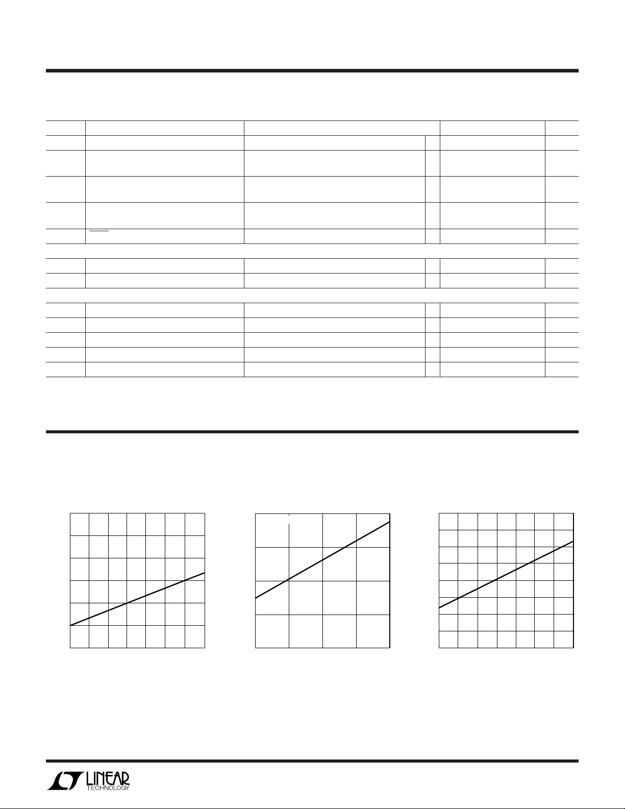
100
I
CHRG
R
SENSE
(CURVES INCLUDE
INPUT DIODE)
90
80
EFFICIENCY (%)
70
60
5
Efficiency vs Input Voltage
= 1.5A
= 68mΩ
= 4V
V
BAT
V
= 3.8V
BAT
10
15
INPUT VOLTAGE (V)
20
400242 TA02
25
400242i
1
LTC4002-4.2
1
2
3
4
8
7
6
5
TOP VIEW
NTC
SENSE
BAT
CHRG
COMP
V
CC
GATE
GND
S8 PACKAGE
8-LEAD PLASTIC SO
TOP VIEW
11
DD PACKAGE
10-LEAD (3mm × 3mm) PLASTIC DFN
10
9
6
7
8
4
5
3
2
1
NC
NTC
SENSE
BAT
CHRG
COMP
V
CC
GATE
PGND
SGND
WW
W
ABSOLUTE AXI U RATI GS
U
(Note 1)
Supply Voltage (VCC) .............................................. 24V
GATE .................................................. (VCC –8V) to V
CC
BAT, SENSE .............................................. –0.3V to 14V
CHRG, COMP, NTC ..................................... – 0.3V to 8V
UUW
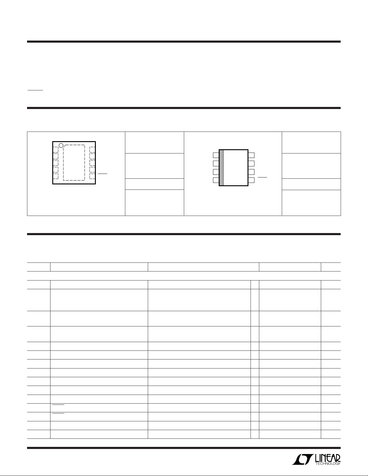
PACKAGE/ORDER I FOR ATIO
ORDER PART
NUMBER
LTC4002EDD-4.2
DD PART MARKING
T
= 125°C, θJA = 43°C/W
JMAX
EXPOSED PAD IS GND (PIN 11)
MUST BE SOLDERED TO PCB
Consult LTC Marketing for parts specified with wider operating temperature ranges.
LAGG
Operating Temperature Range (Note 2) .. – 40°C to 85°C
Storage Temperature Range ................. –65°C to 150°C
Lead Temperature (Soldering, 10 sec).................. 300°C
ORDER PART
NUMBER
LTC4002ES8-4.2
S8 PART MARKING
T
= 125°C, θJA = 110°C/W
JMAX
400242
ELECTRICAL CHARACTERISTICS
temperature range, otherwise specifications are at TA = 25°C. VCC = 10V unless otherwise noted.
SYMBOL PARAMETER CONDITIONS MIN TYP MAX UNITS
DC Characteristics
V
CC
I
CC
V
BAT
V
SNS(CHG)
V
SNS(TRKL)
V
TRKL
V
UV
∆V
UV
V
MSD
V
ASD
I
COMP
I
CHRG
V
CHRG
R
EOC
t
TIMER
2
VCC Supply Voltage ● 4.7 24 V
VCC Supply Current Current Mode 3 5 mA
Battery Regulated Float Voltage 5V ≤ VCC ≤ 24V (Note 2) 4.168 4.2 4.232 V
Constant Current Sense Voltage 3V ≤ V
Trickle Current Sense Voltage V
Trickle Charge Threshold Voltage V
VCC Undervoltage Lockout Threshold Voltage VCC Rising 3.9 4.2 4.5 V
VCC Undervoltage Lockout Hysteresis Voltage 200 mV
Manual Shutdown Threshold Voltage COMP Pin Falling 200 360 500 mV
Automatic Shutdown Threshold Voltage VCC – V
COMP Pin Output Current V
CHRG Pin Weak Pull-Down Current V
CHRG Pin Output Low Voltage I
End-of-Charge Ratio V
Charge Time Accuracy 10 %
The ● denotes the specifications which apply over the full operating
Shutdown Mode 3 5 mA
Sleep Mode 10 20 µA
● 4.158 4.242 V
≤ 4V (Note 3) 0°C ≤ TA ≤ 85°C ● 93 100 107 mV
BAT
= 0V (Note 3) 5 10 15 mV
BAT
Rising 2.75 2.9 3.05 V
BAT
BAT
= 1.2V 100 µA
COMP
= 1V 15 25 35 µA
CHRG
= 1mA 0.15 0.3 V
CHRG
SNS(EOC)/VSNS(CHG)
–40°C ≤ T
≤ 85°C ● 90 110 mV
A
250 mV
10 25 32 %
400242i
LTC4002-4.2
TEMPERATURE (°C)
–50
f
OSC
(kHz)
25
400242 G03
500
–25 0 50
450
550
75 100 125
ELECTRICAL CHARACTERISTICS
The ● denotes the specifications which apply over the full operating
temperature range, otherwise specifications are at TA = 25°C. VCC = 10V unless otherwise noted.
SYMBOL PARAMETER CONDITIONS MIN TYP MAX UNITS
I
NTC
V
NTC-HOT
V
NTC-COLD
∆V
RECHRG
I
LEAK
Oscillator
f
OSC
DC Maximum Duty Cycle 100 %
Gate Drive
t
r
t
f
∆V
GATE
∆V
GATEHI
∆V
GATELO
Note 1: Absolute Maximum Rating are those values beyond which the life
of a device may be impaired.
NTC Pin Output Current V
NTC Pin Threshold Voltage (Hot) V
= 0.85V ● 75 85 95 µA
NTC
Falling ● 340 355 370 mV
NTC
Hysteresis 25 mV
NTC Pin Threshold Voltage (Cold) V
Rising ● 2.428 2.465 2.502 V
NTC
Hysteresis 170 mV
Recharge Battery Voltage Offset from Full V
BAT(FULLCHARGED)
– V
RECHRG
, V
Falling 100 150 200 mV
BAT
Charged Battery Voltage
CHRG Pin Leakage Current V
= 8V, Charging Stops 1 µA
CHRG
Switching Frequency 450 500 550 kHz
Rise Time C
Fall Time C
Output Clamp Voltage VCC – V
Output High Voltage ∆V
Output Low Voltage ∆V
= 2000pF, 10% to 90% 20 ns
GATE
= 2000pF, 90% to 10% 50 ns
GATE
, VCC ≥ 9V ● 8V
GATE
GATEHI
GATELO
= VCC – V
= VCC – V
, VCC ≥ 7V ● 0.3 V
GATE
, VCC ≥ 7V ● 4.5 V
GATE
Note 2: The LTC4002-4.2 is tested with Test Circuit 1.
Note 3: The LTC4002-4.2 is tested with Test Circuit 2.
UW
TYPICAL PERFOR A CE CHARACTERISTICS
Supply Current vs Temperature Supply Current vs V
4.0
3.5
(mA)
CC
I
3.0
2.5
–50
–25 0
50 100 125
25 75
TEMPERATURE (°C)
400242 G01
(mA)
CC
I
4
3
2
CURRENT MODE
5
10
15
VCC (V)
CC
20
TA = 25°C, VCC = 10V unless otherwise noted.
Oscillator Frequency
vs Temperature
25
400242 G02
400242i
3
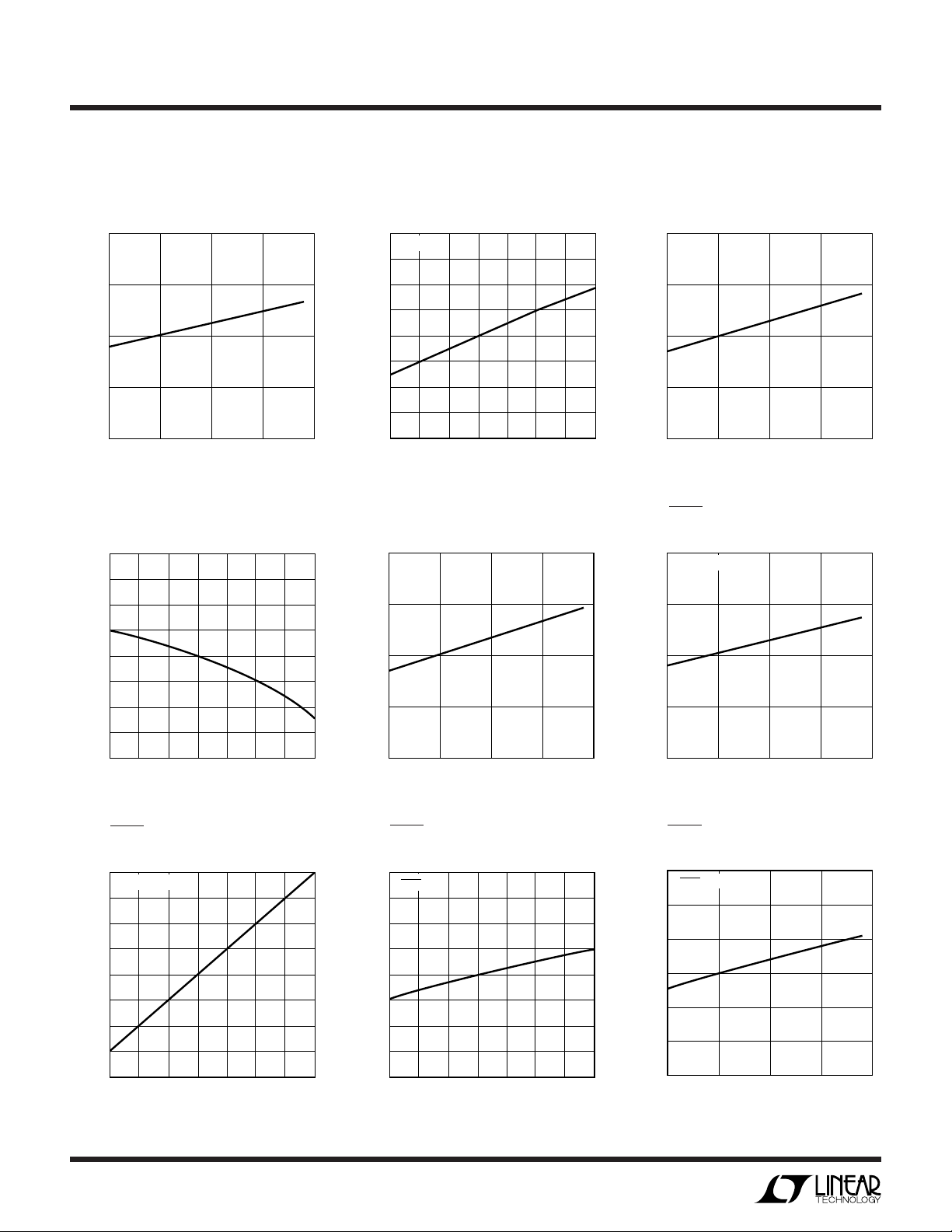
LTC4002-4.2
VCC (V)
5
22
I
CHRG
(µA)
25
28
10 15 20 25
400242 G11
V
CHRG
= 8V
UW
TYPICAL PERFOR A CE CHARACTERISTICS
TA = 25°C, VCC = 10V unless otherwise noted.
Oscillator Frequency vs V
510
(kHz)
500
OSC
f
490
5
10
VCC (V)
Trickle Charge Voltage
vs Temperature
3.0
(V)
2.9
TRKL
V
Current Mode Sense Voltage
CC
15
20
25
400242 G04
vs Temperature
104
V
= 4V
BAT
(mV)
100
SNS
V
96
–25 0 50
–50
25
TEMPERATURE (°C)
75 100 125
400242 G05
Trickle Charge Voltage
vs V
CC
3.0
V
= 4V
BAT
(V)
2.9
TRKL
V
Current Mode Sense Voltage
vs V
CC
102
V
= 4V
BAT
(mV)
100
SNS
V
98
5
10
15
VCC (V)
CHRG Pin Output Low Voltage
vs V
CC
150
I
= 1mA
LOAD
(mV)
140
CHRG
V
20
25
400242 G04
2.8
–25 0 50
–50
25
TEMPERATURE (°C)
75 100 125
400242 G07
CHRG Pin Output Low Voltage
vs Temperature
180
I
= 1mA
LOAD
(mV)
140
CHG
V
100
–25 0 50
–50
4
25
TEMPERATURE (°C)
75 100 125
400242 G10
2.8
5
10
15
VCC (V)
CHRG Pin Weak Pull-Down
Current vs Temperature
29
V
= 8V
CHRG
(µA)
25
CHRG
I
21
–25 0 50
–50
25
TEMPERATURE (°C)
20
400242 G08
75 100 125
400242 G23
25
130
5
10
15
VCC (V)
20
25
400242 G09
CHRG Output Pin Weak Pull-Down
Current vs V
CC
400242i
TEMPERATURE (°C)
–50
I
NTC
(µA)
25
400242 G17
85
–25 0 50
81
89
75 100 125
V
NTC
= 0V
TEMPERATURE (°C)
–50
R
EOC
(%)
25
400242 G20
25
–25 0 50
21
29
75 100 125
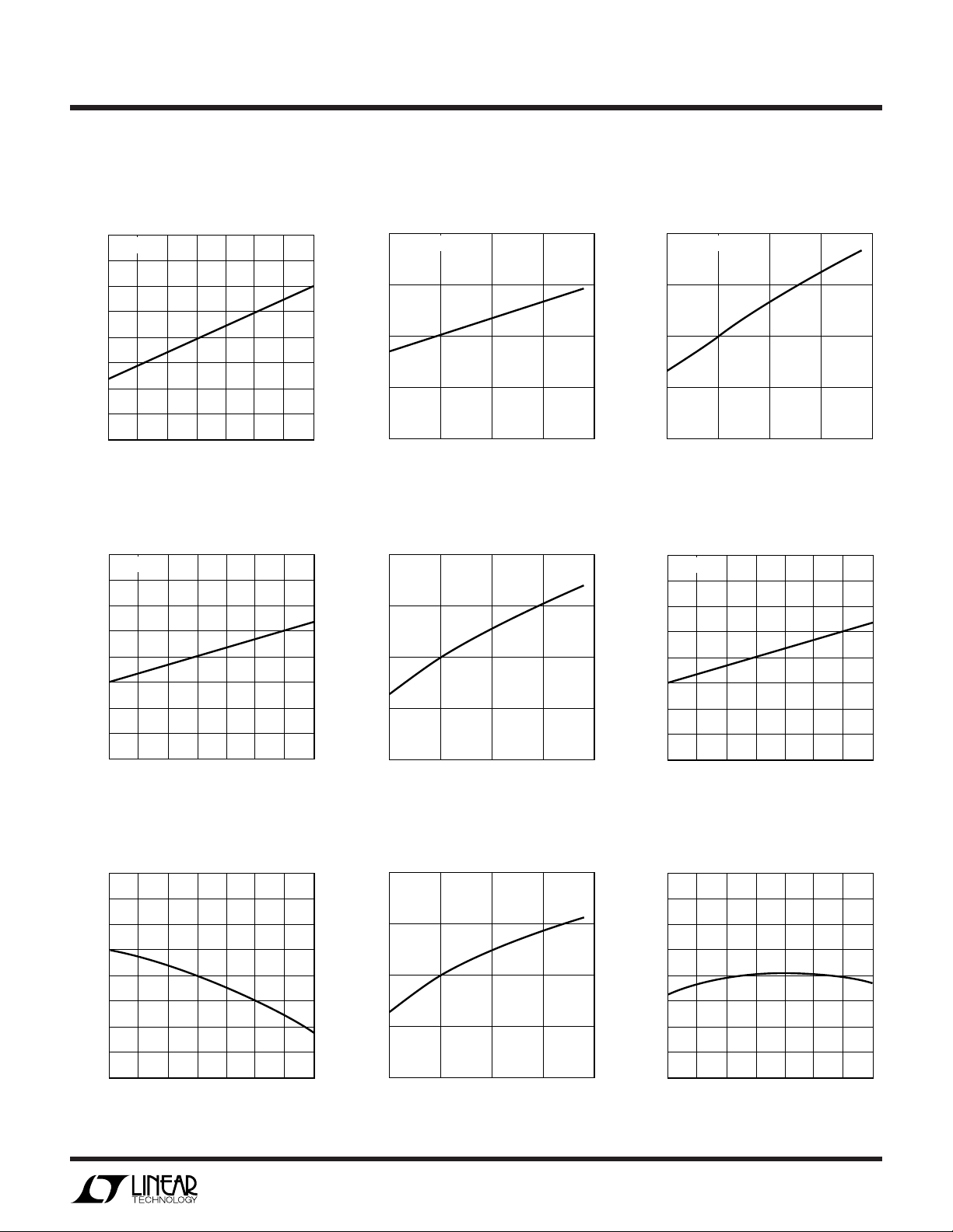
UW
TYPICAL PERFOR A CE CHARACTERISTICS
LTC4002-4.2
TA = 25°C, VCC = 10V unless otherwise noted.
Trickle Charge Sense Voltage
vs Temperature
10.4
V
= 2.5V
BAT
(mV)
10.0
SNS
V
9.6
–25 0 50
–50
25
TEMPERATURE (°C)
COMP Pin Output Current
vs Temperature
104
V
= 0V
COMP
75 100 125
400242 G12
Trickle Charge Sense Voltage
vs V
CC
11
V
= 2.5V
BAT
(mV)
10
SNS
V
9
5
10
15
V
(V)
CC
NTC Pin Output Current
vs V
CC
86
V
= 0V
NTC
COMP Pin Output Current
vs V
CC
102
V
= 0V
COMP
(µA)
100
COMP
I
20
25
400242 G13
98
5
10
15
VCC (V)
20
25
400242 G14
NTC Pin Output Current
vs Temperature
(µA)
100
COMP
I
96
–25 0 50
–50
25
TEMPERATURE (°C)
75 100 125
400242 G15
Recharge Voltage Offset from Full
Charged Voltage vs Temperature
190
(mV)
150
RECHRG
∆V
110
–25 0 50
–50
25
TEMPERATURE (°C)
75 100 125
400242 G18
(µA)
85
NTC
I
84
5
10
15
VCC (V)
Recharge Voltage Offset from Full
Charged Voltage vs V
160
(mV)
150
RECHRG
∆V
140
5
10
CC
15
VCC (V)
20
25
400242 G16
End-of-Charge Ratio
vs Temperature
20
25
400242 G19
400242i
5
 Loading...