

1
LTC4001
4001f
■
Handheld Battery-Powered Devices
■
Handheld Computers
■
Charging Docks and Cradles
■
Digital Cameras
■
Smart Phones
2A Single Cell Li-Ion Battery Charger
2A Synchronous
Buck Li-Ion Charger
■
Low Power Dissipation
■
2A Maximum Charge Current
■
No External MOSFETs, Sense Resistor or Blocking
Diode Required
■
Remote Sensing at Battery Terminals
■
Programmable Charge Termination Timer
■
Preset 4.2V Float Voltage with ±0.5% Accuracy
■
Programmable Charge Current Detection/Termination
■
Automatic Recharge
■
Thermistor Input for Temperature Qualified Charging
■
Compatible with Current Limited Wall Adapters
■
Low Profile 16-Lead (4mm × 4mm) QFN Package
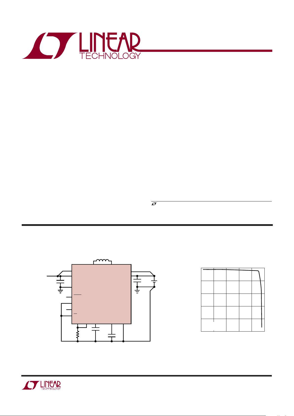
Power Loss vs V
BAT
Charging (PWM Mode)
FEATURES
DESCRIPTIO
U
APPLICATIO S
U
TYPICAL APPLICATIO
U
The LTC®4001 is a 2A Li-Ion battery charger intended for
5V wall adapters. It utilizes a 1.5MHz synchronous buck
converter topology to reduce power dissipation during
charging. Low power dissipation, an internal MOSFET and
sense resistor allow a physically small charger that can be
embedded in a wide range of handheld applications. The
LTC4001 includes complete charge termination circuitry,
automatic recharge and a ±1% 4.2V float voltage. Input
short-circuit protection is included so no blocking diode is
required.
Battery charge current, charge timeout and end-of-charge
indication parameters are set with external components.
Additional features include shorted cell detection, temperature qualified charging and overvoltage protection. The
LTC4001 is available in a low profile (0.75mm) 16-lead
(4mm × 4mm) QFN package.
, LT, LTC and LTM are registered trademarks of Linear Technology Corporation.
All other trademarks are the property of their respective owners.
+
PROG
EN
FAULT
NTC
CHRG
PGND
PV
IN
V
INSENSE
BAT
BATSENS
IDET TIMER
274Ω
0.22µF
10µF
4001 TA01a
4.2V
Li-Ion
10µF
V
IN
4.5V TO 5.5V
0.1µF
SS
SW SENSE
LTC4001
1.5µH
GNDSENS
V
BAT
(V)
3
TOTAL APPLICATION CIRCUIT POWER
DISSIPATION (W)
0.75
1.00
1.25
4
4001 TA01b
0.50
0.25
0
3.25
3.5
3.75
4.25
VIN = 5V
2A CHARGER
2
LTC4001
4001f
Consult LTC Marketing for parts specified with wider operating temperature ranges.
ABSOLUTE AXI U RATI GS
WWWU
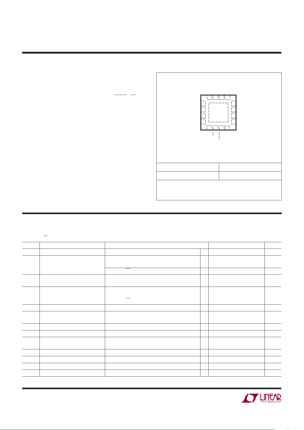
PACKAGE/ORDER I FOR ATIO
UU
W
(Note 1)
LTC4001EUF
ORDER PART NUMBER UF PART MARKING
4001
T
JMAX
= 125°C, θJA = 37°C/W
EXPOSED PAD (PIN 17) IS GND, MUST BE SOLDERED TO PCB
16 15 14 13
5 6 7 8
TOP VIEW
17
UF PACKAGE
16-LEAD (4mm × 4mm) PLASTIC QFN
9
10
11
12
4
3
2
1BAT
SENSE
PGND
GNDSENS
PROG
NTC
FAULT
V
INSENSE
BATSENS
TIMERSSIDET
SW
EN
CHRG
PV
IN
SYMBOL PARAMETER CONDITIONS MIN TYP MAX UNITS
V
IN
Supply Voltage (Note 2) 4 5.5 V
I
IN
PVIN Connected to V
INSENSE
, PROG and IDET 2 mA
Pins Open, Charger On
Shutdown, EN = V
IN
50 µA
V
FLOATVBAT
Regulated Float Voltage Measured from BATSENS to GNDSENS
●
4.158 4.2 4.242 V
4.179 4.2 4.221 V
I
BAT
Current Mode Charge Current R
PROG
= 549Ω, V
BAT
= 3.5V 1.8 2 2.2 A
R
PROG
= 1.10k, V
BAT
= 3.5V 0.9 1 1.1 A
Shutdown, EN = V
IN
±5 µA
I
TRIKL
Trickle Charge Current V
BAT
= 2V 35 50 65 mA
V
TRIKL
Trickle Charge Threshold V
BAT
Rising 3.05 3.1 3.20 V
V
BAT
Falling 2.85 3.0 3.05 V
V
UVL
VIN Undervoltage Lockout Voltage VIN Rising, Measured from V
INSENSE
to GNDSENS 2.7 2.82 V
∆V
UVL
VIN Undervoltage Lockout Hysteresis Measured from V
INSENSE
to GNDSENS 100 mV
V
ASD
Automatic Shutdown Threshold V
INSENSE
– V
BATSENS
Rising (Turn-On), V
BATSENSE
= 4V 200 250 300 mV
Voltage V
INSENSE
– V
BATSENS
Falling (Turn-Off), V
BATSENSE
= 4V 15 30 60 mV
f
OSC
Oscillator Frequency 1.3 1.5 1.7 MHz
D Maximum Duty Factor 100 %
R
PFET
R
DS(ON)
of P-Channel MOSFET Measured from PVIN to SW 127 mΩ
R
NFET
R
DS(ON)
of N-Channel MOSFET Measured from SW to PGND 121 mΩ
The ● denotes specifications which apply over the full operating temperature range, otherwise specifications are TA = 25°C.
V
IN
= 5V, VEN = 0V, R
PROG
= 549Ω, R
IDET
= 549Ω, unless otherwise specified.
ELECTRICAL CHARACTERISTICS
Order Options Tape and Reel: Add #TR
Lead Free: Add #PBF Lead Free Tape and Reel: Add #TRPBF
Lead Free Part Marking: http://www.linear.com/leadfree/
PVIN, V
INSENSE
t < 1ms, DC < 1% .................................... –0.3V to 7V
Steady State ............................................ –0.3V to 6V
SW, SENSE, BAT, BATSENS, SS, FAULT, CHRG, EN,
NTC, PROG, IDET, TIMER Voltage .............. – 0.3V to 6V
Operating Temperature Range (Note 3) .. –40°C to 85°C
Operating Junction Temperature
(Note 5) ............................................... – 40°C to 125°C
Storage Temperature Range ................ –65°C to 125°C

3
LTC4001
4001f
SYMBOL PARAMETER CONDITIONS MIN TYP MAX UNITS
t
TIMER
Timer Accuracy C
TIMER
= 0.22µF ±10 %
V
EN
Enable Input Threshold Voltage VEN Rising 0.6 0.8 1 V
∆V
EN
Enable Input Hysteresis 100 mV
V
PROG
PROG Pin Voltage R
PROG
= 549Ω 1.213 V
V
IDET
IDET Pin Voltage R
IDET
= 549Ω 1.213 V
I
IDET
IDET Threshold R
IDET
= 549Ω 150 200 250 mA
I
CHRG
CHRG Pin Weak Pull-Down Current V
CHRG
= 1V 15 30 50 µA
V
CHRG
CHRG Pin Output Low Voltage I
CHRG
= 5mA 0.2 0.4 V
V
OL
FAULT Pin Output Low Voltage 1mA Load 0.4 V
V
OH
FAULT Pin Output High Voltage 1mA Load 4.6 V
V
RECHRG
Recharge Battery Threshold Voltage V
FLOAT
– V
RECHRG VBAT
Falling 50 100 135 mV
t
RB
Recharge Filter Time Constant 4 ms
t
RECHRG
Recharge Time Percent of Total Charge Time 50 %
t
TRIKL
Low-Battery Trickle Charge Time Percent of Total Charge Time, V
BAT
< 2.8V, 25 %
Measured Using BATSENS and GNDSENS Pins
I
SS
Soft-Start Ramp Current V
BAT
< V
FLOAT
– 100mV, V
BAT
Across BATSENS 6 12.8 16 µA
and GNDSENS Pins
V
COLD
NTC Pin Cold Temperature Fault From NTC to GNDSENS Pin
Threshold Rising Threshold 0.74 V
INSENSE
V
Falling Threshold 0.72 V
INSENSE
V
V
HOT
NTC Pin Hot Temperature Fault From NTC to GNDSENS Pin
Threshold Falling Threshold 0.29 V
INSENSE
V
Rising Threshold 0.30 V
INSENSE
V
V
DIS
NTC Disable Threshold (Falling) From NTC to GNDSENS Pin 0.015 • 0.02 • 0.025 • V
V
INSENSEVINSENSEVINSENSE
∆V
DIS
NTC Disable Hysteresis From NTC to GNDSENS Pin 0.01 • V
INSENSE
V
The ● denotes specifications which apply over the full operating temperature range, otherwise specifications are TA = 25°C.
V
IN
= 5V, VEN = 0V, R
PROG
= 549Ω, R
IDET
= 549Ω, unless otherwise specified.
ELECTRICAL CHARACTERISTICS
Note 1: Stresses beyond those listed under Absolute Maximum Ratings
may cause permanent damage to the device. Exposure to any Absolute
Maximum Rating condition for extended periods may affect device
reliability and lifetime.
Note 2: Operation with current limited wall adapters is allowed down to the
undervoltage lockout threshold.
Note 3: The LTC4001E is guaranteed to meet performance specifications
from 0°C to 85°C. Specifications over the –40°C to 85°C operating
temperature range are assured by design, characterization and correlation
with statistical process controls.
Note 4: T
J
is calculated from the ambient temperature TA and power
dissipation P
D
according to the following formula:
T
J
= TA + (PD • 37°C/W)
Note 5: This IC includes overtemperature protection that is intended to
protect the device during momentary overload. Junction temperature will
exceed 125°C when overtemperature protection is active. Continuous
operation above the specified maximum operating junction temperature
my impair device reliability.
4
LTC4001
4001f
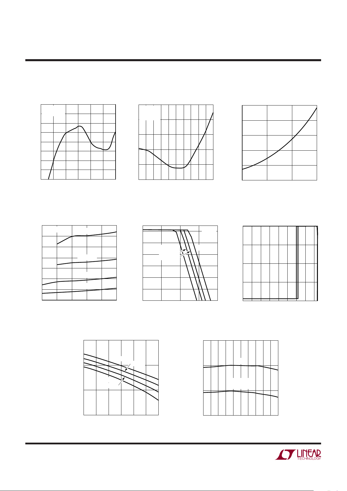
TYPICAL PERFOR A CE CHARACTERISTICS
UW
Oscillator Frequency vs V
IN
Oscillator Frequency
vs Temperature
Dissipation of Figure 8 Circuit
vs I
BAT
PROG Pin Characteristic
(V
PROG
vs I
PROG
)
Dissipation of Figure 8 Circuit
vs V
IN
Trickle Charge Current vs V
BAT
V
FLOAT
and Recharge Battery
Threshold Voltage vs Temperature
Output Charging Characteristic
Showing Constant Current and
Constant Voltage Operation
(T
A
= 25°C unless otherwise noted)
VIN (V)
3
PERCENT VARIATION (%)
–0.25
0
0.25
4.5
5.5
4001 G01
–0.50
–0.75
–1.00
3.5 4 5
0.50
0.75
1.00
6
V
BAT
= 3.2V
V
SS
= 1V
I
PROG
(mA)
0
0.8
1.0
15
4001 G05
0.6
0.4
510 20
0.2
0
1.2
V
PROG
(V)
VIN = 5V
V
BAT
= 3.2V V
BAT
= 4V
V
BAT
= 3.5V
V
BAT
= 3.7V
V
BAT
(V)
0
0
I
BAT
(A)
0.5
1.0
1.5
2.0
0.5 1 1.5 2
4001 G06
2.5 3 3.5 4
V
BAT
(V)
0
40
I
BAT
(mA)
45
50
55
0.5 1 1.5 2
4001 G07
2.5 3
VIN = 5.5V
VIN = 5V
VIN = 4V
VIN = 4.5V
TEMPERATURE (°C)
–50
FREQUENCY VARIATION FROM 25°C (%)
0.4
0.6
0.8
110
4001 G02
0.2
0
–0.2
–30 –10 10
30 50
70 90 130
150
VIN = 5V
V
BAT
= 3.2V
V
SS
= 1V
I
BAT
(mA)
500
TOTAL APPLICATION CIRCUIT POWER
DISSIPATION (W)
0.50
0.75
4001 G03
0.25
0
1000
1500
2000
1.25
1.00
V
IN
= 5V
V
BAT
= 4V
VIN (V)
4.25
1.0
1.2
1.4
5.25
4001 G04
0.8
0.6
4.5 4.75 5 5.5
0.4
0.2
0
TOTAL APPLICATION CIRCUIT POWER
DISSIPATION (W)
I
BAT
= 2A
V
BAT
= 4V
I
BAT
= 1.5A
I
BAT
= 1A
I
BAT
= 500mA
TEMPERATURE (°C)
4.0
FLOAT AND RECHARGE VOLTAGES (V)
4.1
4.2
4.3
–10 30 70 110
4001 G08
150–30–50 10 50 90 130
V
FLOAT
V
RECHARGE
(V
BAT
FALLING)
5
LTC4001
4001f
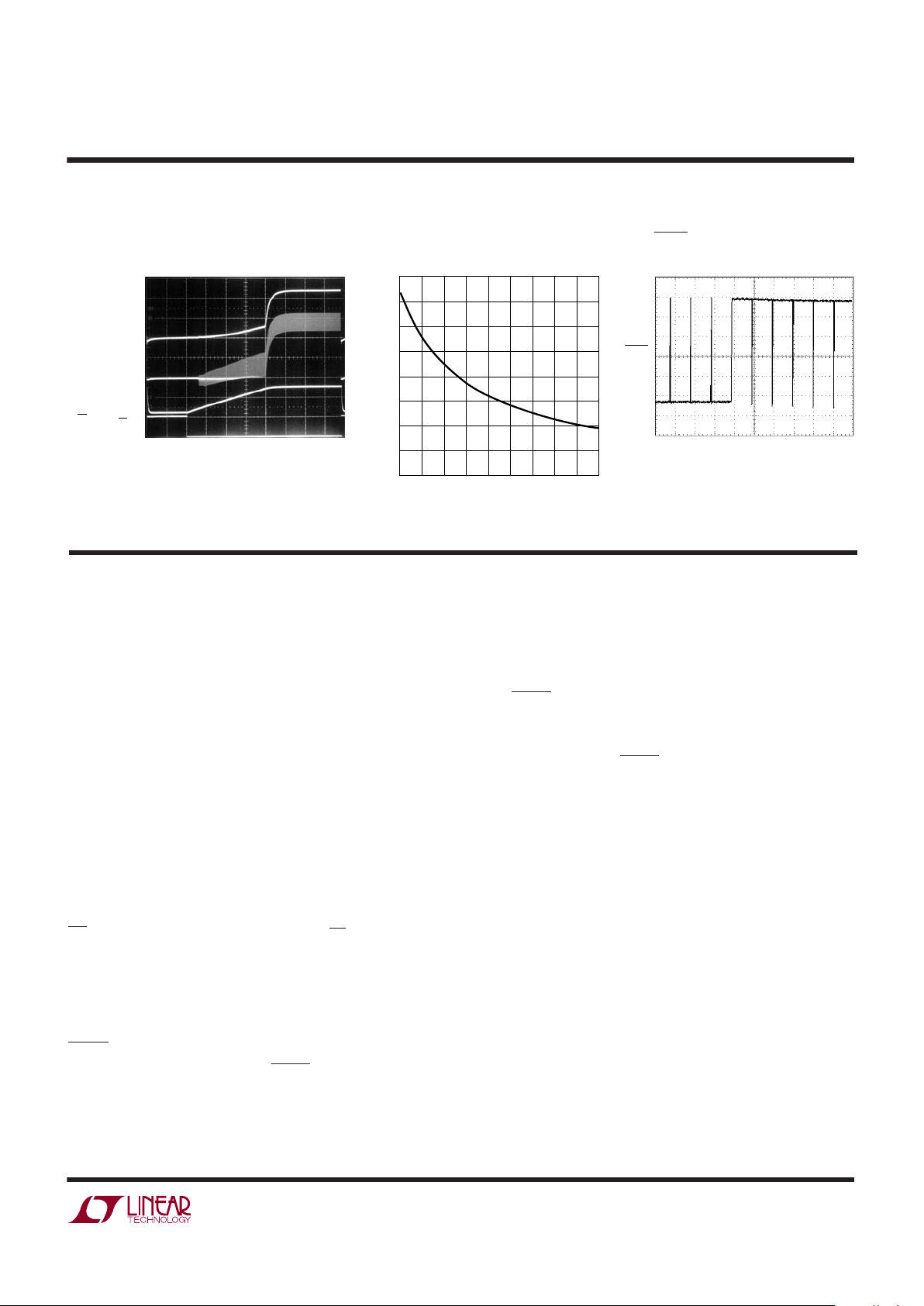
TYPICAL PERFOR A CE CHARACTERISTICS
UW
Soft-Start (PWM Mode)
IDET Threshold vs R
IDET
for
R
PROG
= 549Ω
UU
U
PI FU CTIO S
BAT (Pin 1): Battery Charger Output Terminal. Connect a
10µF ceramic chip capacitor between BAT and PGND to
keep the ripple voltage small.
SENSE (Pin 2): Internal Sense Resistor. Connect to external inductor.
PGND (Pin 3): Power Ground.
GNDSENS (Pin 4): Ground Sense. Connect this pin to the
negative battery terminal. GNDSENS provides a Kelvin
connection for PGND and must be connected to PGND
schematically.
SW (Pin 5): Switch Node Connection. This pin connects to
the drains of the internal main and synchronous power
MOSFET switches. Connect to external inductor.
EN (Pin 6): Enable Input Pin. Pulling the EN pin high places
the LTC4001 into a low power state where the BAT drain
current drops to less than 3µA and the supply current is
reduced to less than 50µA. For normal operation, pull the
pin low.
CHRG (Pin 7): Open-Drain Charge Status Output. When
the battery is being charged, CHRG is pulled low by an
internal N-channel MOSFET. When the charge current
drops below the IDET threshold (set by the R
IDET
programming resistor) for more than 5milliseconds, the N-channel
MOSFET turns off and a 30µA current source is connected
from CHRG to ground. (This signal is latched and is reset
by initiating a new charge cycle.) When the timer runs out
or the input supply is removed, the current source will be
disconnected and the CHRG pin is forced to a high impedance state. A temperature fault causes this pin to blink.
PV
IN
(Pin 8): Positive Supply Voltage Input. This pin
connects to the power devices inside the chip. V
IN
ranges
from 4V to 5.5V for normal operation. Operation down to
the undervoltage lockout threshold is allowed with current
limited wall adapters. Decouple with a 10µF or larger
surface mounted ceramic capacitor.
V
INSENSE
(Pin 9): Positive Supply Sense Input. This pin
connects to the inputs of all input comparators (UVL, V
IN
to V
BAT
). It also supplies power to the controller portion of
this chip. When the BATSENS pin rises to within 30mV of
V
INSENSE
, the LTC4001 enters sleep mode, dropping IIN to
50µA. Tie this pin directly to the terminal of the PV
IN
decoupling capacitor.
CHRG Pin Temperature Fault
Behavior (Detail)
0
INPUT
CURRENT (I
IN
)
0.5A/DIV
INDUCTOR
CURRENT (I
L
)
0.5A/DIV
SOFT-START
VOLTAGE (V
SS
)
1V/DIV
EN PIN (V
EN
)
5V/DIV
0
0
0
2ms/DIVV
BAT
= 3.5V
V
IN
= 5V
4001 G09
R
IDET
(Ω)
300
IDET (mA)
200
250
300
1100
4001 G10
150
100
0
500
700
900
400 1200
600
800
1000
50
400
350
CHRG
1V/DIV
TIME (20µs/DIV)
4001 G11

6
LTC4001
4001f
FAULT (Pin 10): Battery Fault. This pin is a logic high if a
shorted battery is detected or if a temperature fault is
detected. A temperature fault occurs with the temperature
monitor circuit enabled and the thermistor temperature is
either below 0°C or above 50°C (typical).
NTC (Pin 11): Input to the NTC (Negative Temperature
Coefficient) Thermistor Temperature Monitoring Circuit.
Under normal operation, tie a thermistor from the NTC pin
to the GNDSENS pin and a resistor of equal value from NTC
to VIN. When the voltage on this pin is above 0.74VIN (Cold,
0°C) or below 0.29V
IN
(Hot, 50°C), charging is disabled
and the CHRG pin blinks. When the voltage on NTC comes
back between 0.74V
IN
and 0.29VIN, the timer continues
where it left off and charging resumes. There is approximately 3°C of temperature hysteresis associated with
each of the input comparators. If the NTC function is not
used connect the NTC pin to GNDSENS. This will disable
all of the NTC functions. NTC should never be pulled above
VIN.
PROG (Pin 12): Charge Current Program. The R
PROG
resistor connects from this pin to GNDSENS, setting the
current:
R
k
I
PROG
BAT AMPS
=
1 110.
()
where I
BAT
is the high rate battery charging current.
UU
U
PI FU CTIO S
IDET (Pin 13): Charge Rate Detection Threshold. Connecting a resistor, R
IDET
to GNDSENS programs the charge
rate detection threshold. If R
IDET
= R
PROG
, CHRG provides
an I
BAT
/10 indication. For other thresholds see the Appli-
cations Information section.
SS (Pin 14): Soft-Start/Compensation. Provides soft-start
function and compensation for the float voltage control
loop and compensation for the charge current control
loop. Tie a soft-start/compensation capacitor between this
pin and GNDSENS.
TIMER (Pin 15): Timer Capacitor. The timer period is set
by placing a capacitor, C
TIMER
, to GNDSENS. Set C
TIMER
to:
C
TIMER
= Time (Hrs) • 0.0733 (µF)
where time is the desired charging time.
Connect this pin to IDET to disable the timer. Connect this
pin to GNDSENS to end battery charging when I
BAT
drops
below the IDET charge rate threshold.
BATSENS (Pin 16): Battery Sense Input. An internal resistor divider sets the final float voltage at this pin. The
resistor divider is disconnected in sleep mode or when
EN = H to reduce the battery drain current. Connect this pin
to the positive battery terminal.
Exposed Pad (Pin 17): Ground. This pin must be soldered
to the PCB ground (PGND) for electrical contact and rated
thermal performance.
 Loading...