

FEATURES
■
N-Channel Synchronous MOSFET Driver
■
Programmable Timeout
■
Reverse Inductor Current Sense
■
Gate Drive Transformer Synchronization
Sequence Monitor
■
Wide VCC Supply Range: 4.5V to 11V
■
15ns Rise/Fall Times at VCC = 5V, CL = 4700pF
■
Undervoltage Lockout
■
Small 16-Lead SSOP Package
U
APPLICATIO S
■
48V Input Isolated DC/DC Converters
■
Isolated Telecom Power Supplies
■
Distributed Power Step-Down Converters
■
Industrial Control System Power Supplies
■
Automotive and Heavy Equipment
LTC3901
Secondary Side
Synchronous Driver for Push-Pull
and Full-Bridge Converters
U
DESCRIPTIO
The LTC®3901 is a secondary side synchronous rectifier
driver designed to be used in isolated push-pull and fullbridge converter power supplies. The chip drives two
external N-channel MOSFETs and accepts a transformergenerated bipolar input to maintain sychronization with
the primary side controller.
The LTC3901 provides a full range of protection features
for the external MOSFETs. A programmable timeout function is included that disables both drivers when the synchronization signal is missing or incorrect. Additionally,
the chip senses the output inductor current through the
drain-source resistance of the two MOSFETs, turning off
the MOSFETs if the inductor current reverses. The LTC3901
also shuts off the drivers if the supply is low or if the
synchronization sequence is incorrect.
, LTC and LT are registered trademarks of Linear Technology Corporation.
All other trademarks are the property of their respective owners.
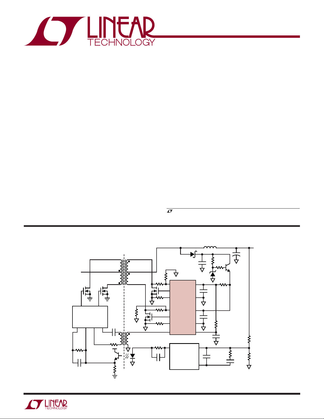
TYPICAL APPLICATIO
V
IN
36V TO 72V
MA MB ME
DRVA DRVB
LTC3723
PUSH-PULL
CONTROLLER
COMP V
FB
U
ISOLATION
BARRIER
T1
+
CSE
ME
CSE
CSF
MF
SDRBSDRA
T2
MF
CSF
SYNC
OUT
LT4430 OR LT1431
V
–
GND
LTC3901
+
PV
–
PGND
TIMER
OPTOCOUPLER
DRIVER
COMP
CC
CC
L1
+
FB
C
3901 F01
OUT
V
12V
OUT
Figure 1. Simplified Isolated Push-Pull Converter
3901f
1
LTC3901
TOP VIEW
GN PACKAGE
16-LEAD NARROW PLASTIC SSOP
1
2
3
4
5
6
7
8
16
15
14
13
12
11
10
9
PV
CC
ME
ME
PGND
CSE
–
CSE
+
TIMER
GND
V
CC
MF
MF
PGND
CSF
–
CSF
+
GND
SYNC
ABSOLUTE AXI U RATI GS
(Note 1)
Supply Voltage
, PV
V
CC
Input Voltage
–
CSE
, CSF–, TIMER ................. –0.3V to (VCC + 0.3V)
SYNC ...................................................... –12V to 12V
Input Current
CSE+, CSF
Operating Temperature Range (Note 2) ...–40°C to 85°C
Storage Temperature Range ..................–65°C to 150°C
Lead Temperature (Soldering, 10 sec).................. 300°C
ELECTRICAL CHARACTERISTICS
temperature range. V
SYMBOL PARAMETER CONDITIONS MIN TYP MAX UNITS
V
CC
V
UVLO
I
VCC
Timer
V
TMR
I
TMR
t
TMRDIS
V
TMRMAX
Current Sense (Note 5)
ICS+CS
ICS–CS
V
CSMAX
V
CS
SYNC Input
I
SYNC
V
SYNCP
V
SYNCN
Driver Output
R
ONH
R
ONL
I
PK
2
WW
W
............................................................................
CC
+
.....................................................................
= 5V, TA = 25°C unless otherwise specified. (Note 3)
CC
Supply Voltage Range ● 4.5 5 11 V
VCC Undervoltage Lockout Threshold Rising Edge ● 4.1 4.5 V
V
Undervoltage Lockout Hysteresis Rising Edge to Falling Edge 0.5 V
CC
VCC Supply Current V
Timer Threshold Voltage ● –10% VCC/5 10% V
Timer Input Current V
Timer Discharge Time C
Timer Pin Clamp Voltage C
+
Input Current VCS+ = 0V ● ±1 µA
–
Input Current VCS– = 0V ● ±1 µA
CS+ Pin Clamp Voltage IIN = 5mA, Driver Off 11 V
Current Sense Threshold Voltage VCS– = 0V 7.5 10.5 13.5 mV
SYNC Input Current V
SYNC Input Positive Threshold ● 1.0 1.4 1.8 V
SYNC Positive Input Hysteresis (Note 7) 0.2 V
SYNC Input Negative Threshold ● –1.8 –1.4 –1.0 V
SYNC Negative Input Hysteresis (Note 7) 0.2 V
Driver Pull-Up Resistance I
Driver Pull-Down Resistance I
Driver Peak Output Current (Note 7) 2 A
U
UUW
PACKAGE/ORDER I FOR ATIO
ORDER PART
12V
15mA
T
= 125°C, θJA = 130°C/W
JMAX
Consult LTC Marketing for parts specified with wider operating temperature ranges.
The ●
denotes specifications which apply over the full operating
= 0V ● 0.5 1 mA
SYNC
f
= 100kHz, CME = CMF = 4700pF (Note 4) ● 715 mA
SYNC
= 0V ● –6 –10 µA
TMR
= 1000pF, R
TMR
= 1000pF, R
TMR
(Note 6)
= ±10V ● ±1 ±10 µA
SYNC
= –100mA 0.9 1.2 Ω
OUT
= 100mA 0.8 1.2 Ω
OUT
= 4.7k ● 40 120 ns
TMR
= 4.7k 2.5 V
TMR
● 318mV
● 1.6
● 1.6
NUMBER
LTC3901EGN
GN PART
MARKING
3901
3901f
LTC3901
ELECTRICAL CHARACTERISTICS
temperature range.
V
= 5V, TA = 25°C unless otherwise specified. (Note 3)
CC
The ●
denotes specifications which apply over the full operating
SYMBOL PARAMETER CONDITIONS MIN TYP MAX UNITS
Switching Characteristics (Note 8)
t
d
tr, t
f
Note 1: Absolute Maximum Ratings are those values beyond which the life
of a device may be impaired.
Note 2: The LTC3901E is guaranteed to meet performance specifications
from 0°C to 70°C. Specifications over the –40°C to 85°C operating
temperature range are assured by design; characterization and correlation
with statistical process controls.
Note 3: All currents into device pins are positive; all currents out of device
pins are negative. All voltages are referenced to ground unless otherwise
specified.
Note 4: Supply current in normal operation is dominated by the current
needed to charge and discharge the external MOSFET gates. This current
SYNC Input to Driver Output Delay CME = CMF = 4700pF, V
Driver Rise/Fall Time CME = CMF = 4700pF, V
will vary with supply voltage, switching frequency and the external
MOSFETs used.
Note 5: Both CSE
the same performance specifications.
Note 6: The current sense comparator threshold has a 0.33%/°C
temperature coefficient (TC) to match the TC of the external MOSFET
R
DSON
Note 7: Guaranteed by design, not subject to test.
Note 8: Rise and fall times are measured using 10% and 90% levels. Delay
times are measured from ±1.4V at SYNC input to 20%/80% levels at the
driver output.
= ±5V ● 60 120 ns
SYNC
= ±5V 15 ns
SYNC
+
, CSE– and CSF+, CSF– current sense comparators have
.
UW
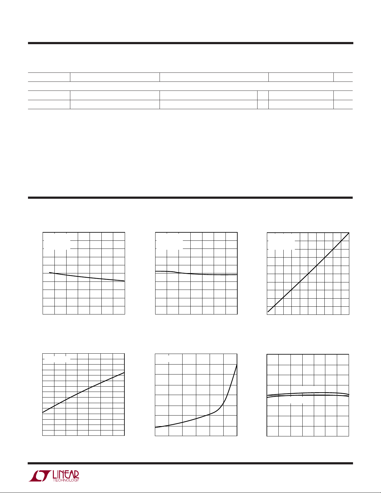
TYPICAL PERFOR A CE CHARACTERISTICS
Timeout vs V
5.25
TA = 25°C
5.20
R
TMR
C
TMR
5.15
5.10
5.05
5.00
4.95
TIMEOUT (µs)
4.90
4.85
4.80
4.75
4
5
= 51k
= 470pF
CC
8
7
6
VCC (V)
Current Sense Threshold vs
Temperature
18
VCC = 5V, 11V
17
16
15
14
13
12
11
10
9
8
7
6
5
CURRENT SENSE THRESHOLD (mV)
4
3
–50 100
050–25 25 75 125
TEMPERATURE (°C)
Timeout vs Temperature
5.25
VCC = 5V
5.20
5.15
5.10
5.05
5.00
4.95
TIMEOUT (µs)
4.90
4.85
4.80
10
11
3901 G01
9
4.75
= 51k
R
TMR
= 470pF
C
TMR
–50 0
–25
V
CS(MAX)
50
25
TEMPERATURE (°C)
75
100
Clamp Voltage vs CS
125
3901 G02
+
Input Current
18
TA = 25°C
17
16
15
14
CLAMP VOLTAGE (V)
13
12
CS(MAX)
V
11
3901 G04
10
05
10 2015
+
CS
INPUT CURRENT (mA)
25
30
3901 G05
Timeout vs R
10
TA = 25°C
9
= 5V
V
CC
= 470pF
C
TMR
8
7
6
5
4
TIMEOUT (µs)
3
2
1
0
0 10203040506070 8090100
TMR
R
TMR
(kΩ)
SYNC Positive Threshold vs
Temperature
1.8
1.7
1.6
1.5
1.4
1.3
1.2
SYNC POSITIVE THRESHOLD (V)
1.1
1.0
–25 25 75 125
–50
VCC = 11V
VCC = 5V
050
TEMPERATURE (°C)
3901 G03
100
3901 G06
3901f
3
LTC3901
UW
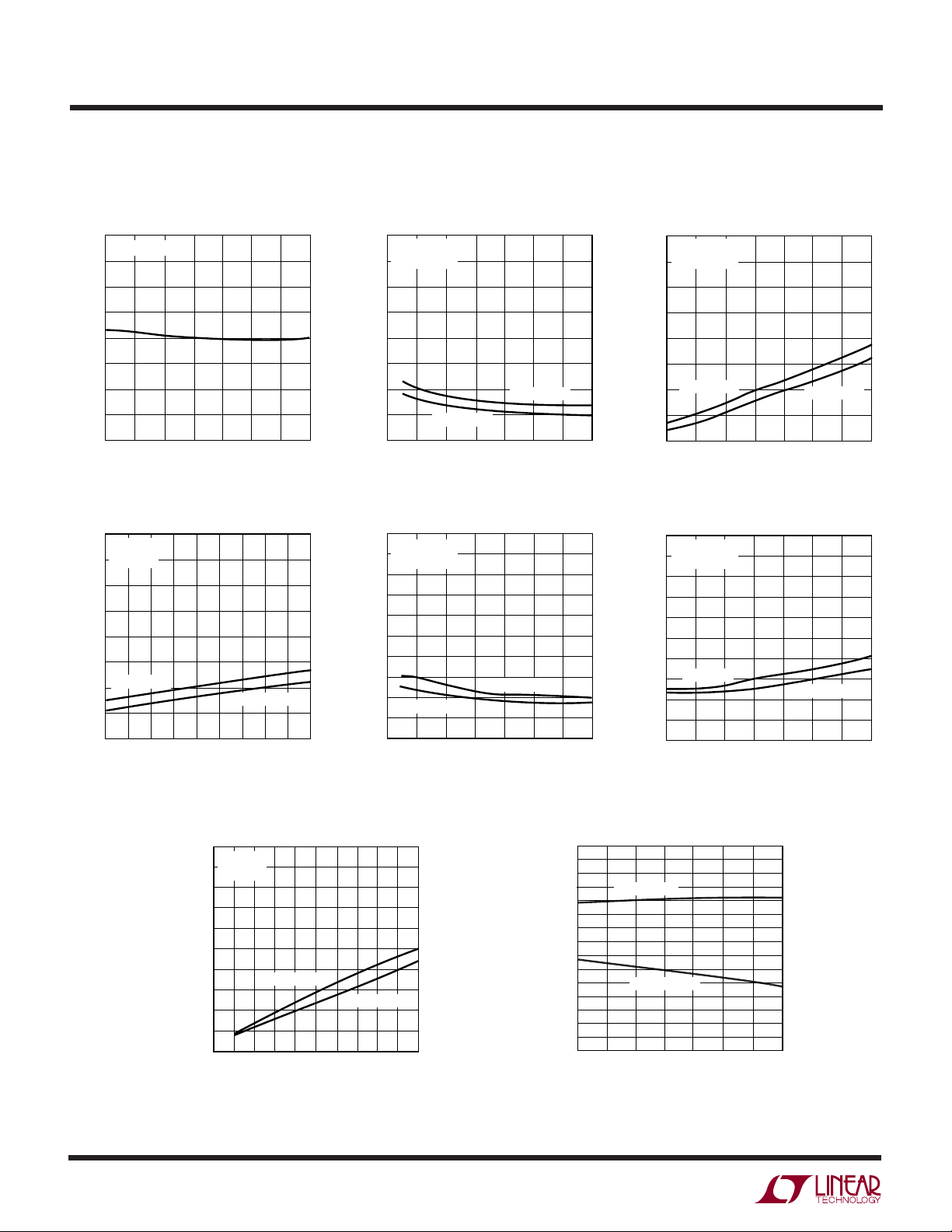
TYPICAL PERFOR A CE CHARACTERISTICS
SYNC Negative Threshold vs
Temperature Propagation Delay vs V
–1.0
VCC = 5V, 11V
–1.1
–1.2
–1.3
–1.4
–1.5
–1.6
SYNC NEGATIVE THRESHOLD (V)
–1.7
–1.8
–50
Propagation Delay vs C
120
TA = 25°C
V
110
100
90
80
70
SYNC TO ME
60
PROPAGATION DELAY (µs)
50
40
123 10
050
–25 25 75 125
TEMPERATURE (°C)
LOAD
= 5V
CC
SYNC TO MF
4567 98
C
(nF)
LOAD
100
3901 G07
3901 G10
120
TA = 25°C
= 4.7nF
C
110
LOAD
100
90
80
70
60
PROPAGATION DELAY (µs)
50
40
4
SYNC TO MF
57911
68
Rise/Fall Time vs V
50
TA = 25°C
45
40
35
30
25
20
15
RISE/FALL TIME (ns)
10
= 4.7nF
C
LOAD
FALL TIME
5
0
410
6857911
Rise/Fall Time vs Load
Capacitance
50
TA = 25°C
45
= 5V
V
CC
40
35
30
25
20
15
RISE/FALL TIME (ns)
10
5
0
RISE TIME
FALL TIME
1023 104567 98
C
(nF)
LOAD
V
V
(V)
CC
(V)
CC
CC
SYNC TO ME
10
3901 G08
CC
RISE TIME
3901 G11
Undervoltage Lockout Threshold
Voltage vs Temperature
4.5
4.4
4.3
4.2
4.1
4.0
3.9
3.8
3.7
3.6
VOLTAGE (V)
3.5
3.4
3.3
3.2
UNDERVOLTAGE LOCKOUT THRESHOLD
3.1
3.0
–50 100
RISING EDGE
FALLING EDGE
Propagation Delay vs
Temperature
120
VCC = 5V
= 4.7nF
C
110
LOAD
100
90
80
70
SYNC TO ME
60
PROPAGATION DELAY (µs)
50
40
–50 100
050–25 25 75 125
TEMPERATURE (°C)
Rise/Fall Time vs Temperature
50
VCC = 5V
45
40
35
30
25
20
15
RISE/FALL TIME (ns)
10
5
0
050–25 25 75 125
TEMPERATURE (°C)
= 4.7nF
C
LOAD
RISE TIME
–50 100
050–25 25 75 125
TEMPERATURE (°C)
3901 G143901 G13
SYNC TO MF
3901 G09
FALL TIME
3901 G12
4
3901f
UW
TYPICAL PERFOR A CE CHARACTERISTICS
V
Supply Current vs
CC
Temperature
20
C
= 4.7nF
LOAD
18
16
14
12
10
SUPPLY CURRENT (mA)
8
CC
V
6
4
–50 100
VCC = 11V
VCC = 5V
050–25 25 75 125
TEMPERATURE (°C)
3901 G15
30
25
20
15
10
SUPPLY CURRENT (mA)
V
Supply Current
CC
vs Load Capacitance
TA = 25°C
5
0
1023 104567 98
C
LOAD
LTC3901
VCC = 11V
VCC = 5V
(nF)
3901 G16
U
UU
PI FU CTIO S
P
VCC (Pin 1): Driver Supply Input. This pin powers the
ME and MF drivers. Bypass this pin to PGND using a 4.7µF
low ESR capacitor in close proximity to the LTC3901. This
pin should be connected to the same supply voltage as the
VCC pin.
ME (Pin 2, 3): Driver Output for ME. This pin drives the
gate of the external N-channel MOSFET, ME.
PGND (Pin 4,13): Power Ground. Both drivers return to
this pin. Connect PGND to a high current ground node in
close proximity to the sources of ME and MF.
CSE+, CSE– (Pin 6, 5): ME Current Sense Differential
Input. Connect CSE+ through a series resistor to the drain
of ME and CSE– through a series resistor to the source of
ME. The LTC3901 monitors the CSE inputs 250ns after ME
goes high. If the inductor current reverses and flows into
ME causing CSE+ to rise above CSE– by more than 10.5mV,
the LTC3901 pulls ME low. See the Current Sense section
for more details on choosing the resistance values for
R
to R
CSE1
TIMER (Pin 7): Timer Input. Connect this pin to an external
R-C network to program the timeout period. The LTC3901
resets the timer at every positive and negative transition of
the SYNC input. If the SYNC signal is missing or incorrect,
the LTC3901 pulls both ME and MF low once the TIMER
pin goes above the timeout threshold. See the Timer section for more details on programming the timeout period.
CSE3
.
GND (Pin 8,10): Signal Ground. All internal low power
circuitry returns to this pin. To minimize differential ground
currents, connect GND to PGND right at the LTC3901.
SYNC (Pin 9): Driver Synchronization Input. 0V at this pin
forces both ME and MF high after an initial negative pulse.
A subsequent positive pulse at SYNC input forces ME to
pull low, whereas a negative pulse forces MF to pull low.
The SYNC signal should alternate between positive and
negative pulses. If the SYNC signal is incorrect, the LTC3901
pulls both MF and ME low.
CSF+, CSF– (Pin 11, 12): MF Current Sense Differential
Input. Connect CSF+ through a series resistor to the drain
of MF and CSF– through a series resistor to the source of
MF. The LTC3901 monitors the CSF inputs 250ns after MF
goes high. If the inductor current reverses and flows into
MF causing CSF+ to rise above CSF– by more than 10.5mV,
the LTC3901 pulls MF low. See the Current Sense section
for more details on choosing the resistance values for
R
CSF1
to R
CSF3
.
MF (Pin 14, 15): Driver Output for MF. This pin drives the
gate of the external N-channel MOSFET, MF.
VCC (Pin 16): Power Supply Input. All internal circuits
except the drivers are powered from this pin. Bypass this
pin to GND using a 1µF capacitor in close proximity to the
LTC3901.
3901f
5

LTC3901
BLOCK DIAGRA
9
SYNC
+
CSE
6
–
CSE
5
+
CSF
11
–
CSF
12
TIMER
7
W
10.5mV
+
–
10.5mV
+
–
+1.4V
–1.4V
Z
11V
CSF
Z
11V
S
S
ISE
CSE
ISF
TMR
+
–
SYNC
–
SYNC
AND
DRIVER
LOGIC
TIMER
RESET
R1
180k
DISABLE
DRIVER
UVLO
V
16
CC
PV
1
CC
3
ME
4
PGND
14
MF
13
PGND
+
SYNC
R2
45k
M
U
TMR
Z
TMR
0.5 • V
CC
WUU
APPLICATIO S I FOR ATIO
Overview
Push-pull and full bridge converters use power transformers to provide input-to-output isolation and voltage stepup/down. Diodes are used as a simple solution for secondary side rectification. Unfortunately, as output currents
increase, the loss associated with diode forward voltage
drop results in low overall efficiency. The LTC3901 overcomes this problem by providing control and drive for two
external N-channel synchronous MOSFETs. Synchronization to the primary side controller is maintained through a
small signal transformer.
Figure 1 shows a simplified push-pull converter application. T1 is the power transformer; MA and MB are the
primary side power transistors driven by the LTC3723
controller’s DRVA and DRVB outputs. The gate drive
transformer T2 is driven by the LTC3723’s SDRA and
SDRB outputs and provides the synchronization signal to
the LTC3901 on the secondary side. When both SDRA and
SDRB are high, there is no voltage across the transformer’s
primary and the LTC3901 SYNC input is approximately 0V.
According to the polarity of the transformer: if SDRA goes
low while SDRB is high, SYNC is positive; if SDRB goes
low while SDRA is high, SYNC is negative. ME and MF are
108
3901 BD
GND GND
the secondary side synchronous switches driven by the
LTC3901’s ME and MF output. Inductor L1 and capacitor
C
form the output filter, providing DC output voltage to
OUT
the load. The feedback path from V
through the opto-
OUT
coupler driver and optocoupler back to the primary side
controller is also shown in Figure 1.
Each full cycle of the push-pull converter consists of four
distinct periods. Figure 2 shows the push-pull converter
waveforms.
DRVA
DRVB
SDRA
SDRB
SYNC
ME
MF
Figure 2. Push-Pull Converter Switching Waveforms
0V
3901 F02
3901f
6

WUUU
APPLICATIO S I FOR ATIO
LTC3901
In the first period, SDRA goes low (followed by DRVA
going high) and T2 generates a positive voltage at the
LTC3901’s SYNC input. The LTC3901’s ME output then
pulls low. Current flows to the load through MOSFET MF,
T1’s secondary and L1.
In the second period, SDRA goes high and T2 provides
approximately 0V at the LTC3901 SYNC input. This causes
the LTC3901’s ME output to go high and both MOSFET ME
and MF to conduct. This is the free-wheeling period with
T1 secondary winding shorted.
In the third period, SDRB goes low (followed by DRVB
going high) and T2 generates a negative voltage at the
LTC3901’s SYNC input. The LTC3901’s MF output then
pulls low. Current flows to the load through MOSFET ME,
T1’s secondary and L1.
The last period is also a free-wheeling period like the
second period. Both SDRA and SDRB are high and the
LTC3901 forces both MOSFETs ME and MF to conduct.
External MOSFET Protection
A programmable timer and two differential input current
sense comparators are included in the LTC3901 for protection of the external MOSFETs during power down and
Burst Mode® operation. The chip also shuts off the
MOSFETs if V
< 4.1V or if the synchronization sequence
CC
is incorrect.
When the primary controller is powering down, the
LTC3901 continues to operate by drawing power from the
V
bypass cap, C
CC
. The primary controller synchro-
VCC
nous output stops switching and the LTC3901 SYNC input
goes to 0V. Both ME and MF remain on and the decreasing
inductor current continues to flow into the load. Once the
inductor current decreases to zero, it reverses direction,
discharging the output capacitor C
both MOSFETs. At the same time, the C
to GND through
OUT
voltage contin-
VCC
ues to drop. When the voltage drops below 4.1V, the
LTC3901 shuts down and pulls both ME and MF low. This
causes the inductor current to stop suddenly and the drain
voltage of both MOSFETs to fly high, due to the buildup of
inductor energy. In the absence of a protection timer, if the
inductor energy is high due to a long period of current
reversal, the drain voltage can go above the MOSFET’s
voltage rating and cause damage to the MOSFET.
MOSFETs are also kept on for long periods when the
primary controller enters Burst Mode operation. Both ME
and MF stop switching until the primary controller exits
Burst Mode operation. This would also cause the inductor
current to reverse and the drains to fly high.
In both of these situations, the timer and/or current sense
comparator shuts off the drivers before or immediately
after the inductor current reverses direction. This prevents
the buildup of inductor energy.
Timer
The timer circuit (Figure 3) operates by using an external
R-C charging network to program the timeout period. On
every transition at the SYNC input, the chip generates a
200ns pulse to reset the timer capacitor. If the SYNC signal
is missing or incorrect (allowing the timer capacitor voltage to go high) it shuts off both drivers once the voltage
reaches the timeout threshold. Figure 4 shows the timer
waveforms.
V
CC
TIMER
RESET
16
V
CC
TIMER
Z
TMR
0.5 • V
CC
M
TMR
7
3901 F03
R
TMR
32k
C
TMR
470pF
TIMEOUT
THRESHOLD
3901 F02
0V
SYNC
ME
MF
TIMER RESET
(INTERNAL)
TIMER
LTC3901
TMR
TIMEOUT
R1
180k
R2
45k
Figure 3. Timer Circuit
Burst Mode is a registered trademark of Linear Technology Corporation.
Figure 4. Timer Waveforms
3901f
7

LTC3901
SYNC
ME
MF
3901 F05
0V
EXPECTED POSITIVE SYNC PULSE,
MF PULLS HIGH
SECOND NEGATIVE SYNC PULSE,
BOTH ME AND MF PULL LOW
U
WUU
APPLICATIO S I FOR ATIO
The timeout period is determined predominantly by the
external R
TMR
and C
VCC voltage. This independence is achieved by making the
timeout threshold a ratio of V
internally by R1 and R2 (see Figure 3). The Timeout period
should be programmed to around 1 period of the primary
switching frequency using the following formula:
TIMEOUT = 0.2 • R
To reduce error in the timeout setting due to the discharge
time, select C
a C
TMR
R
. C
TMR
TMR
around 470pF and then calculate the required
should be placed as close as possible to the
TMR
LTC3901 with minimum PCB trace between C
TIMER pin and GND. This is to reduce any ringing caused
by the PCB trace inductance when C
ringing may introduce error to the timeout setting.
The timer input also includes a current sinking clamp
circuit (Z
in Figure 3) that clamps this pin to about
TMR
0.5 • VCC if there is missing SYNC/timer reset pulse. This
clamp circuit prevents the timer capacitor from getting
fully charged up to the rail, which would result in a longer
discharge time. The current sinking capability of the circuit
is around 1mA.
The timeout function can be disabled by connecting the
timer pin to GND.
values and is independent of the
TMR
. The ratio is 0.2x, set
CC
TMR
• C
+ 0.27E-06
TMR
between 100pF and 1000pF. Start with
, the
TMR
discharges. This
TMR
polarity. In some situations, for example during power-up
or power-down, the SYNC pulse magnitude may be low
(slightly higher or lower than the threshold of the comparators). This can cause only one of the SYNC comparators to
trip. This also appears as a double pulse to the sequential
logic and both drivers will be shut off.
Current Sense
The differential input current sense comparators, ISE and
ISF (Figure 6), are used for sensing the voltage across the
drain-to-source terminal of the MOSFET through the CSX
+
and CSX– pins. There are two sets of comparator inputs,
one for each MOSFET (ME and MF). If the inductor current
reverses into the MOSFET causing CSX+ to rise above
CSX– by more than 10.5mV, the LTC3901 turns off the
respective MOSFET. This comparator is used to prevent
inductor reverse current buildup during power-down or
Burst Mode operation, which may cause damage to the
MOSFETs. The 10.5mV input threshold has a positive
temperature coefficient, which closely matches the TC of
the external MOSFET R
. The current sense com-
DS(ON)
parator is only active 250ns after the respective driver
Synchronization Sequence
A typical push-pull converter cycle always turns off ME
and MF alternately. The SYNC input should alternate
between a positive and negative pulse. The LTC3901
includes a sequential logic to monitor the SYNC input
pulses. If after one positive pulse the SYNC comparator
receives another positive pulse, the LTC3901 sequential
logic shuts off both drivers until a negative pulse appears.
The same applies to double negative pulses; the driver will
turn on only after receiving a positive pulse. This is to
protect the external components in situations where only
one polarity of the SYNC pulse is present and the corresponding driver remains on. Figure 5 shows the SYNC
double pulse operation.
The LTC3901 has two separate SYNC comparators (S+ and
S– in the Block Diagram) to detect the positive and negative pulses. The threshold voltages of both comparators
are designed to be of the same magnitude but opposite in
8
Figure 5. SYNC Double Pulse Operation
T1
ME
R
CSF1
MF
R
CSF3
Figure 6. Current Sense Circuit
R
R
CSE1
CSE3
R
R
CSE2
CSF2
+
CSE
6
10.5mV
–
CSE
CSF
CSF
+
–
+
–
LTC3901
10.5mV
+
–
5
11
12
Z
11V
Z
11V
ISE
CSE
ISF
CSF
3901 F06
3901f

LTC3901
U
WUU
APPLICATIO S I FOR ATIO
output goes high; this is to avoid any ringing immediately
after the MOSFETs are switched on.
Under no/light load conditions, if the inductor average
current is less than half of its peak-to-peak ripple current,
the inductor current will reverse into MOSFETs during a
portion of the free-wheeling period, forcing CSX
above CSX
–
. The current sense comparator input threshold is set at 10.5mV to prevent tripping under this normal
no load condition. If at no load, the product of the inductor
negative peak current and MOSFET R
DS(ON)
10.5mV; this may trip the comparator and force the
LTC3901 to operate in discontinuous mode. Figure 7
shows the LTC3901 operating in discontinuous mode; the
driver’s output goes low before the next SYNC transition
edge when the inductor current goes negative. In pushpull topology, both MOSFETs conduct the same amount of
current during the free-wheeling period; this will trip both
comparators at the same time. Discontinuous mode is
sometimes undesirable because if the load current sud-
SDRA
SDRB
SYNC
ME
MF
L1
CURRENT
CURRENT SENSE
COMPARATOR TRIP
Figure 7a. Discontinuous Mode Operation at No Load
SYNC
+
to rise
is higher than
0V
0V
0V
denly increases when the MOSFETs are off, it creates a
large output voltage drop. To overcome this, add a resistor
divider, R
CSX1
and R
at the CSX+ pin to increase the
CSX2
10.5mV threshold so that the LTC3901 operates in continuous mode at no load.
The LTC3901 CSX+ pin has an internal current sinking
clamp circuit (Z
) that clamps the pin to around 11V.
CSX
The clamp circuit, together with the external series resistor R
1, protects the CSX
CSX
+
pins from the high MOSFET
drain voltage in the power delivery cycle. During the power
delivery cycle, one of the MOSFETs (ME or MF) is off. The
drain voltage of the MOSFET that is off is determined by the
primary input voltage and the transformer turn ratio. This
voltage can be high and may damage the internal circuit if
CSX+ is connected directly to the drain of its MOSFET. The
current sinking capability of the clamp circuit is 5mA
minimum.
The value of the resistorsR
CSX1
, R
CSX2
and R
CSX3
should
be calculated using the following formulas to meet both
the clamp and threshold voltage requirements:
k = {48 • I
R
= {200 • V
CSX2
R
= k • R
CSX1
R
= {R
CSX3
If k = 0 or less than zero, R
= R
CSX3
RIPPLE
CSX2
CSX1
= {V
• R
DS(ON)
IN(MAX)
• R
CSX2
IN(MAX)
} –1
• NS/NP –2200 • (1 + k)} /k
} / {R
CSX2
CSX1
+ R
CSX2
}
is not needed and R
• (NS/NP) – 11V} / 5mA
CSX1
where:
I
R
V
= Inductor peak-to-peak ripple current
RIPPLE
= On-resistance of MOSFET at I
DS(ON)
IN(MAX)
= Primary side main supply maximum input
RIPPLE
/2
voltage
NS/NP = Power transformer T1, turn ratio
ME
MF
CURRENT
L1
ADJUSTED CURRENT SENSE THRESHOLD
Figure 7b. Continuous Mode Operation
with Adjusted Current Sense Threshold
0V
3901 F06
If the LTC3901 still operates in discontinuous mode with
the calculated resistance value, increase the value of
R
to raise the threshold. The resistors R
CSX1
R
and the CSX+ pins input capacitance plus the PCB
CSX2
CSX1
and
trace capacitance forms an R-C delay; this slows down the
response time of the comparators. The resistors and CSX
+
input leakage currents also create an input offset error.
To minimize this delay and error, do not use resistance
value higher than required and make the PCB trace from
3901f
9

LTC3901
3901 F09
D3
MBR0540
T1
SECONDARY
WINDING
0.1µF
R
Z
2k
R
B
OPTIONAL
Q
REG
FZT690B
C
PVCC
4.7µF
C
VCC
1µF
PV
CC
V
CC
6V
D
Z
R
VCC
100Ω
U
WUU
APPLICATIO S I FOR ATIO
the resistors to the LTC3901 CSX+/CSX– pins as short as
possible . Add a series resistor, R
parallel sum of R
connect the other end of R
CSX1
and R
CSX3
CSX2
directly to the source of the
MOSFET.
SYNC Input
Figure 8 shows the external circuit for the LTC3901 SYNC
input. The gate drive transformer (T2) should be selected
based on the primary switching frequency and SDRA/
SDRB output voltage.
The values of the C
and R
SG
SYNC
to obtain a optimum SYNC pulse shape and amplitude. The
amplitude of the SYNC pulse should be much higher than
the LTC3901 SYNC threshold of ±1.4V. Amplitudes greater
than ±5V will help to speed up the SYNC comparator and
reduce the propagation delay from SYNC to the drivers.
When SDRA and SDRB lines go low, the resulting undershoot or overshoot must not exceed the minimum SYNC
threshold of ±1V.
C
SG
0.1µF
SDRB
PRIMARY
CONTROLLER
SDRA
R
SG
220Ω
Figure 8. SYNC Input Circuit
VCC/PVCC Regulator
The VCC/PVCC supply for the LTC3901 can be generated by
peak rectifying the transformer secondary winding as
shown in Figure 9. The Zener diode DZ sets the output
voltage (VZ – 0.7V). Resistor RB (on the order of a few
hundred ohms), in series with the base of Q
required to surpress high frequency oscillations depending on Q
’s selection. A power MOSFET can also be used
REG
by increasing the zener diode value to offset the drop of the
gate-to-source voltage. The VCC input is separated from
the PVCC input through a 100Ω resistor. This lowers the
driver switching feedthrough. Connect a 1µF bypass ca-
pacitor for the VCC supply. PVCC supply current varies
linearly with the supply voltage, driver load and clock
frequency. A 4.7µF bypass capacitor for the PVCC supply
is sufficient for most applications. Alternatively, the
LTC3901 can be powered directly by V
10
, with value equal to
CSX3
to the CSX– pin and
should then be adjusted
T2
LTC3901
SYNC
R
SYNC
4.7k
3901 F08
REG
if the voltage is
OUT
, may be
Figure 9. VCC/PVCC Regulator
higher than 4.5V. This reduces the number of external
components needed.
The LTC3901 has an UVLO detector that pulls the drivers’
output low if V
V
= 1V to 4.1V. The UVLO detector has 0.5V of hyster-
CC
< 4.1V. The output remains off from
CC
esis to prevent chattering.
In a typical push-pull converter, the secondary side cir-
cuits have no power until the primary side controller starts
operating. Since power for the LTC3901 is derived from
the power transformer T1, the LTC3901 will initially remain off. During this period (V
< 4.1V), the synchronous
CC
MOSFETs ME and MF will remain off and the MOSFETs’
body diodes will conduct. The MOSFETs may experience
very high power dissipation due to a high voltage drop in
the body diodes. To prevent MOSFET damage, a V
CC
voltage greater than 4.1V should be provided quickly. The
V
supply circuit in Figure 9 will provide power for the
CC
LTC3901 within the first few switching pulses of the
primary controller, preventing overheating of the MOSFETs.
Full-Bridge Converter Application
The LTC3901 can be used in full-bridge converter applications. Figure 10 shows a simplified full-bridge converter
circuit. The LTC3901 circuit and operation is the same as
in the push-pull application (refer to Figure 1). On the primary side there are four power MOSFETs, MA to MD, driven
by the respective outputs of the primary controller. Transformer T3 and T4 step up the gate drives for MA and MC.
Each full cycle of the full-bridge converter includes four
distinct periods which are similar to those found in the
push-pull application. Figure 11 shows the full-bridge
converter switching waveforms. The shaded areas correspond to power delivery periods.
3901f

WUUU
the
APPLICATIO S I FOR ATIO
V
IN
MA
T3
MB
ISOLATION
BARRIER
MC
T4
MD
LTC3901
L1
+
T1
L2
C
OUT
V
OUT
AB CD
LTC3722-1
FULL-BRIDGE CONTROLLER
COMP V
MA
MB
MC
MD
E
FB
FE
6
+
CSE
3
ME
MF
T2
ME
5
CSE
11
CSF
14
MF
12
CSF
9
SYNC
OUT
OPTOCOUPLER
–
LTC3901
+
–
DRIVER
V
CC
GND
PV
CC
PGND
TIMER
FB
COMP
16
8,10
1
4,13
7
Figure 10. Simplified Isolated Full-Bridge Converter
In the first period, MB turns off, E goes low (followed by
MA turning on), and the LTC3901 forces ME to turn off.
The primary side delivers power to the load through
MOSFET MF, T1 and L1.
In the second period, MA remains on, MD turns off, and
MC turns on. E goes high and the LTC3901 forces both ME
and MF to conduct. This is the free-wheeling period with
the T1 secondary output shorted.
3901 F10
F
SYNC
ME
MF
0V
3901 F11
Figure 11. Full-Bridge Converter Switching Waveforms
In the third period, MA turns off, F goes low (followed by
MB turning on), and the LTC3901 forces MF to turn off.
The primary side delivers power to the load through
MOSFET ME, T1 and L2.
Like the second period, the last period is a free-wheeling
period. MB remains on, MC turns off, MD turns on, F goes
high, and the LTC3901 forces both ME and MF to conduct.
The timeout and current sense operations are the same as
in the push-pull application.
3901f
11

LTC3901
U
WUU
APPLICATIO S I FOR ATIO
MOSFET Selection
The required MOSFET R
based on allowable power dissipation and maximum required output current.
The MOSFETs body diodes conduct during the power-up
phase, when the LTC3901 V
ME and MF signals stay low and the inductor current flows
through the body diodes. The body diodes must be able to
handle the load current during start-up until V
4.1V.
The LTC3901 drivers dissipate power while the MOSFETs
are switching. The power dissipation increases with switching frequency, PVCC, and size of the MOSFETs. To calculate the driver dissipation, the total gate charge QG is used.
This parameter is found on the MOSFET manufacturers’
data sheets.
The power dissipated in each LTC3901 MOSFET driver is:
P
where fSW is the switching frequency of the converter.
= QG • PVCC • f
DRIVER
should be determined
DS(ON)
supply is ramping up. The
CC
CC
SW
reaches
PC Board Layout Checklist
When laying out the printed circuit board, the following
checklist should be used to ensure proper operation of the
LTC3901:
1. Connect the 1µF C
possible to the V
C
bypass capacitor as close as possible to the PV
PVCC
and PGND pins.
2. Connect the two MOSFET drain terminals directly to the
transformer. The two MOSFET sources should be as close
together as possible.
3. Keep the timer, SYNC and VCC regulator circuit away
from the high current path of ME, MF and T1.
4. Place the timer capacitor, C
the LTC3901.
5. Keep the PCB trace from the resistors R
R
to the LTC3901 CSX+/CSX– pins as short as pos-
CSX3
sible. Connect the other ends of the resistors directly to the
drain and source of the MOSFET.
CC
bypass capacitor as close as
VCC
and GND pins. Connect the 4.7µF
CC
as close as possible to
TMR
CSX1
, R
CSX2
and
6. Make the connection between GND and PGND right at
the LTC3901 pins.
12
3901f

L6 0.65µH
1µF
V
OUT
V
E
V
F
–V
OUT
–V
OUT
8.5V
100Ω
C4
3.3µF
50V
390pF
1µF
100Ω
2k
1/4W
Q1
D6
9.1V
C1, C2, C3
470µF
6.3V
×3
Si7892DP
×3
Si7892DP
×3
1
8
49
11
V
F
V
F
5
3901 TA01
V
OUT
–V
OUT
D1
470Ω
1W
D2
100k
1k
T1
9:9:7:1:1
T2
1(1.5mH):0.5
T1
9T(150µH):9T:7T:1T:1T
••
0.1µF
330pF
C7
2.2nF
250V
+
C5
68µF
20V
+
12
11
8
7
10
9
2
4
5
6
3
1
22Ω
360Ω
L4
1mH
D4
D5
–V
OUT
V
OUT
330Ω
47Ω
0.68µF
D7
1µF, 100V TDK C3225X7R2A105M
C1-C3: SANYO 6TPB470M
C4: TDK C3225X7R1H335M
C5: AVX TPSE686M020R0150
C6: TAIYO YUDEN TMK432BJ106KM
C7: MURATA DE2E3KH222MB3B
D1, D2: DIODES INC. ES1A
D4, D5: BAS21
D6: MMBD5239B
D7: BAT54
L4: COILCRAFT DO1608C-105
L5: VISHAY IHLP-2525CZ-01
L6: PULSE PA1294.650
Q1: FZT690B
Q2: FMMT3904
R1, R2: IRC LRC-LR2512-01-R060-G
T1: EFD25 TRANSPOWER TTI8696
T2: PULSE PA0785
Q2
Si7450DPSi7450DP
80Ω
1W
100pF
200V
80Ω
1W
100pF
200V
470Ω
R1
0.06Ω
1.5W
R2
0.06Ω
1.5W
L5
1µH
1µF
100V
×3
1µF
100V
V
IN
V
IN
–V
IN
3
42610
6
5
18
1
9
14
13
7
12
16
8
3
11
5
15
6
58
1
2
V
OUT
10V
8.5V
787Ω
100Ω
220pF
4.99k
1/4W
270Ω
2.49k
0.022µF
47nF
–V
OUT
GND-F
V
+
GND-S
COLL REF
LT1431CS8
SYNC PV
CC
CSF
+
LTC3901EGN
MOC207
0.1µF
LTC3723EGN-1
V
REF
DPRGSSFBGNDR
LEB
SPRGC
T
DRVB SDRB
SDRA
COMP
V
CC
UVLO
DRVA CS
820Ω
150k
30k
5V
33k
10k
0.47µF
68nF
220pF
1µF
100pF
100Ω
1/4W
10V
66.5k
V
IN
5V
383k
75k
12
4.99k
CSF
–
14
8
4
10 13
MF
15
MF
6
V
E
4.99k
1/4W
CSE
+
5
4.99k
40.2k
CSE
–
GND PGND GND PGND
7
TIMER
2
ME
316
1
ME V
CC
1µF
••
••
•
TYPICAL APPLICATIO S
165W 36V-72V Input to 3.3V at 50A Isolated Push-Pull Converter
LTC3901
U
3901f
13

LTC3901
5
46
A
B
11V12VV
IN
MMBT3904
15
LTC3723EGN-2
DRVB
SDRB
SDRA
COMP
V
CC
UVLO
12
62k
330pF
12V
MMBZ5242B
150pF
1
0.47µF
1µF
DRVA
DPRG V
REF
RAMP SPRG GND SSCS FBC
T
470pF
0.47µF
4.7k
0.22µF
2N7002
B
CS
+
T3
1(1.5mH):0.5
T1
5:4:4:2:2
1µF
8913
1k
22Ω
0.1µF
C1
2.2nF
250V
1µF
100V
1µF
100V
1µF
100V
1µF
100V
0.22µF
Si7370DP
×2
Si7852DP
×2
1
6
5
42
3
A
Si7370DP
×2
1500pF
100V
L2 0.22µH
L3
1mH
C3
68µF
V
F
•
•
11
3
2
8
19
5
4
16
10k
120Ω
30.1k
7
10
14
7.5Ω
D4 D5
7.5Ω
220pF
100Ω
10k
3k
4.7k
1/4W
100pF
215k
15k
1/4W
SYNC PV
CC
CSF
+
V
F
LTC3901EGN
CSF
–
8
11 12
1
41013 7
1µF
1µF
3901 TA02
–V
OUT
10V
MMBZ5240B
1k
V
OUT
MF MF
GND PGND GND PGND TIMER
V
CC
330pF
14 15
10k
3k
33.2k 100Ω
4.7k
1/4W
CSE
+
V
E
20Ω 1W
–V
OUT
V
OUT
V
OUT
–V
OUT
CSE
–
65
ME ME
23 16
MMBT3904
Si7852DP
×2
L1
0.56µH
72
4
CS
+
T2
70(980µH):1
8
7
1
3
12V
D2
D1
D3
3
5
1
6
•
••
•
•
•
•
9
11
V
E
+
LTC4440ES6
BOOSTIN
+
TG
TSGND
V
CC
11V
1µF
100V
V
IN
V
IN
–V
IN
48V
IN
1µF
100V
C2
180µF
16V
+
1µF
1µF, 100V TDK C4532X7R2A105M
C1: MURATA DE2E3KH222MB3B
C2: SANYO 16SP180M
C3: AVX TPSE686M020R0150
D1-D3: BAS21
D4, D5: MMBD914
L1: COILCRAFT DO1813P-561HC
L2: SUMIDA CDEP105-0R2NC-50
L3: COILCRAFT DO1608C-105
T1: PULSE PA0801.005
T2: PULSE P8207
T3: PULSE PA0785
U
TYPICAL APPLICATIO S
240W 42V-56V Input to Unregulated 12V Half-Bridge Converter
14
3901f

LTC3901
5
46
A
B
12V
V
IN
15
LTC3723EGN-1
DRVB
SDRB
SDRA
COMP
CS
V
CC
UVLO
9
150k
1
0.47µF
1µF
DRVA
DPRG V
REF
SPRGGND SSFB C
T
330pF
22nF
100k
D8
10V
68nF
270pF
T2
1(1.5mH):0.5
T1
4T:6T(65µHMIN):6T:2T:2T
243k
2.49k
9.53k
10k
750Ω
1k
100Ω
1/4W
813
3
Si7370DP
×2
L4
1mH
C3
68µF
20V
V
F
•
•
3
2
8
19
5
4
16
10k
33k
200Ω
1/4W
R1
0.03Ω
1.5W
66.5k
RLEB
12
7
14
220pF
22nF
100Ω
665Ω
1k
866Ω
6.19k
1/4W
1.5nF
464k
30k
1/4W
SYNC PV
CC
CSF
+
V
F
LTC3901EGN
CSF
–
8
11 12
1
41013 7
1µF
4.7µF
3901 TA03
–V
OUT
V
OUT
–V
OUT
D7
10V
V
OUT
MF MF
GND PGND GND PGND TIMER
V
CC
470pF
22nF
14 15
1k
866Ω
42.2k
100Ω
MMBT3904
1k
6.19k
1/4W
CSE
+
V
E
–V
OUT
V
OUT
V
F
V
OUT
12V/20A
–V
OUT
CSE
–
65
ME ME
23 16
Si7370DP
×2
Si7852DPSi7852DP
L5
0.56µH
112
4
12V
D5
D6
3
5
1
6
•
••
•
•
9
7
V
E
+
0.1µF
1
6
5
4
B
2
A
D3
LTC4440ES6
BOOSTIN
+
TG
TSGND
V
CC
12V
3
0.1µF
Si7852DP Si7852DP
1
6
5
42
B
D4
LTC4440ES6
BOOSTIN
+
TG
TSGND
V
CC
12V
1µF
100V
×3
V
IN
V
IN
–V
IN
42V TO 56V
1µF
100V
C1, C2
47µF
16V
×2
+
1µF
1µF
100V
1µF, 100V TDK C3225X7R2A105M
C1, C2: SANYO 16TQC47M
C3: AVX TPSE686M020R0150
C4: MURATA GHM3045X7R222K-GC
D2: DIODES INC. ES1B
D3-D6: BAS21
D7, D8: MMBZ5240B
L4: COILCRAFT DO1608C-105
L5: COILCRAFT DO1813P-561HC
L6: PULSE PA1294.132 OR
PANASONIC ETQP1H1R0BFA
R1, R2: IRC LRC2512-R03G
T1: PULSE PA0805.004
T2: PULSE PA0785
6
10
I
SNS
I
SNS
0.1µF
11
58
1
2
1
MOC207
C4
2.2nF
250V
0.1µF
3
6
5
8
GND-F
V
+
GND-S
COLL REF
LT1431CS8
A
1.5k
22Ω
4.7Ω
4.7Ω
R2
0.03Ω
1.5W
V
F
D2
470pF
100V
L6
1.25µH
1k
1/4W
10Ω
1W
6
93
EFFICIENCY (%)
94
95
96
97
81012
LOAD CURRENT (A)
EFFICIENCY
14
16 18 20
42V
IN
48V
IN
56V
IN
U
TYPICAL APPLICATIO S
3901f
15
Information furnished by Linear Technology Corporation is believed to be accurate and reliable.
However, no responsibility is assumed for its use. Linear Technology Corporation makes no representation that the interconnection of its circuits as described herein will not infringe on existing patent rights.
240W 42V-56V Input to 12V at 20A Isolated 1/4 Brick (2.3" × 1.45")

LTC3901
PACKAGE DESCRIPTIO
U
GN Package
16-Lead Plastic SSOP (Narrow .150 Inch)
(Reference LTC DWG # 05-08-1641)
.045 ±.005
.254 MIN
RECOMMENDED SOLDER PAD LAYOUT
.007 – .0098
(0.178 – 0.249)
.016 – .050
NOTE:
1. CONTROLLING DIMENSION: INCHES
2. DIMENSIONS ARE IN
3. DRAWING NOT TO SCALE
*DIMENSION DOES NOT INCLUDE MOLD FLASH. MOLD FLASH
SHALL NOT EXCEED 0.006" (0.152mm) PER SIDE
**DIMENSION DOES NOT INCLUDE INTERLEAD FLASH. INTERLEAD
FLASH SHALL NOT EXCEED 0.010" (0.254mm) PER SIDE
(0.406 – 1.270)
INCHES
(MILLIMETERS)
.150 – .165
.0250 BSC.0165 ± .0015
.015 ± .004
(0.38 ± 0.10)
0° – 8° TYP
× 45°
.229 – .244
(5.817 – 6.198)
.0532 – .0688
(1.35 – 1.75)
.008 – .012
(0.203 – 0.305)
TYP
16
15
12
.189 – .196*
(4.801 – 4.978)
14
12 11 10
13
5
4
3
678
.0250
(0.635)
BSC
.009
(0.229)
9
(0.102 – 0.249)
REF
.150 – .157**
(3.810 – 3.988)
.004 – .0098
GN16 (SSOP) 0204
RELATED PARTS
PART NUMBER DESCRIPTION COMMENTS
LTC1693 High Speed Single/Dual N-Channel MOSFET Drivers CMOS Compatible Input, VCC Range: 4.5V to 13.2V
LTC1698 Isolated Secondary Synchronous Rectifier Controller Use with the LT1681, Optocoupler Driver, Pulse
Transformer Synchronization
LT1952 Synchronous DC/DC Forward Controller Programmable Volt-Second Clamp and Slope Compensation
LTC3722 Synchronous Dual Mode Phase Modulated Full-Bridge Controller 50W to 2kW Power Supply Design, Adaptive Direct Sense ZVS
LTC3723 Synchronous Push-Pull Controller Adjustable Push-Pull Dead Time, High Efficiency
LTC3900 Synchronous Rectifier Driver for Forward Converters Similar Function to the LTC3901 but for Forward Converter
LTC4441 6A MOSFET Driver Adjustable Gate Drive Voltage, Programmable Blanking
LT4430 Optocoupler Driver SOT-23, Prevents Overshoot
LT/TP 1104 1K • PRINTED IN USA
16
Linear Technology Corporation
1630 McCarthy Blvd., Milpitas, CA 95035-7417
(408) 432-1900 ● FAX: (408) 434-0507
●
www.linear.com
© LINEAR TECHNOLOGY CORPORATION 2003
3901f
 Loading...