

Bootstrap Biasing of High Input Voltage Step-Down Controller
Increases Converter Efficiency
Design Note 493
Goran Perica and Victor Khasiev
Introduction
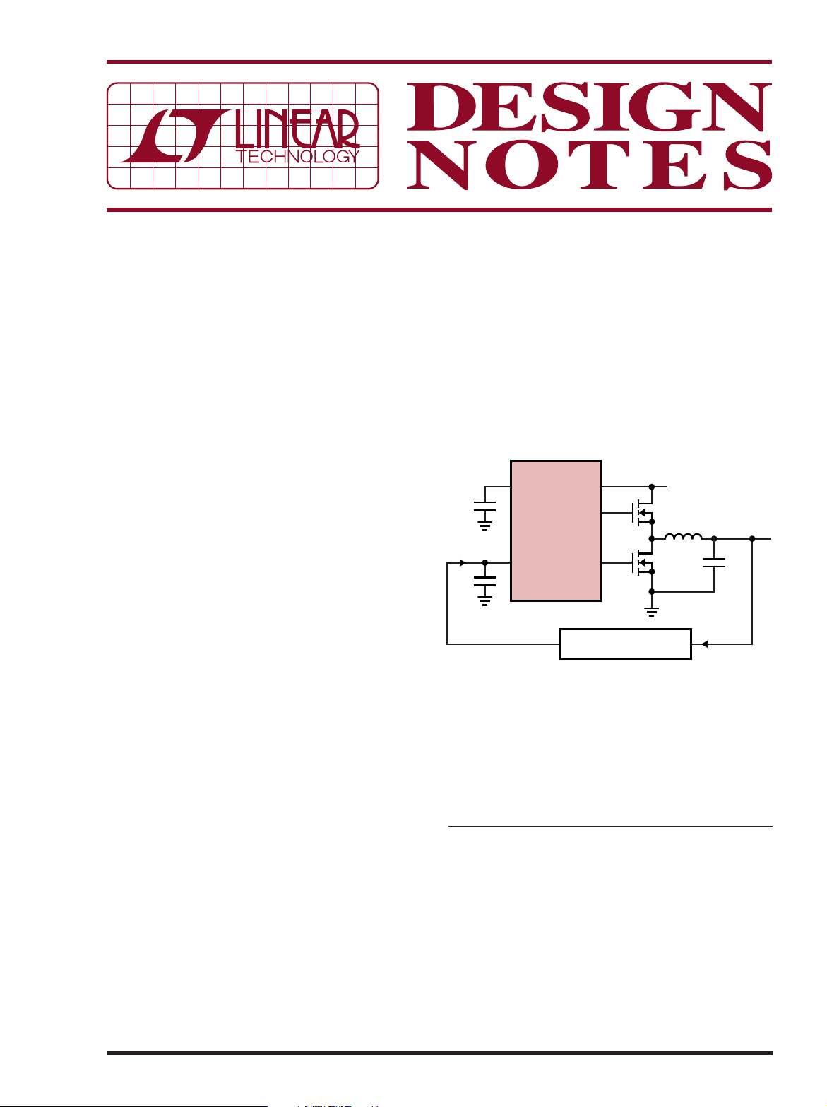
High voltage buc k DC/DC controller s such as the LTC3890
(dual output) and LTC3891 (single output) are popular in
automotive applications due to their extremely wide 4V to
60V input voltage range, eliminating the need for a snubber and voltage suppression circuitry. These controllers
are also well suited for 48V telecom applications where
no galvanic isolation is required.
In a typical application for these controllers, the IC’s
supply voltage (INTV
) is provided by the on-chip LDO.
CC
This LDO produces 5V from input voltages up to 60V to
bias control circuitry and provide power FET gate drive.
Although simple, this built-in biasing scheme can be inefficient. Power losses can be significant in applications
where the input voltage is consistently high, such as in
48V telecom applications. Reducing the power losses
in the bias conversion can increase efficiency and also
reduce the controller case operating temperature.
Employing EXTVCC to Improve Efficiency
One of the at tractive feat ures of the LTC3890 and LTC3891
controllers is the external power input (EXTV
). This is
CC
a second on-chip LDO, which can be used to bias the
chip. When the input voltage is consistently high, it is
more efficient to produce the biasing voltage by stepping down the converter’s output voltage, which is fed
into EXTV
, rather than generating 5V INTVCC from the
CC
high input voltage.
Figure 1 shows a block diagr am for this scheme. The output
can be directly connected to the EXT V
pin of the chip as
CC
long as the output voltage is above 4.7V. However, extra
circuitry (described in the following section) is required
for outputs below 4.7V.
INTV
CC
LTC3890
LTC3891
EXTV
CC
Figure 1. Block Diagram Showing External Bias
VIN (4.5V to 60V)
VOLTAGE DOUBLER OR BOOST
(FIGURE 2 OR FIGURE 3)
V
OUT
DN493 F01
(< 4.7V)
Voltage Doubler for Output Voltages Below 4.7V
When the controller’s output is below 4.7V, it must be
stepped up to allow the built-in LDO to work. A simple
voltage doubler solves this problem as long as the output
is higher than 2.5V. Below 2.5V output, a multivibratorbased circuit can be used.
L, LT, LTC, LTM, Linear Technology, and the Linear logo are registered trademarks of
Linear Technology Corporation. All other trademarks are the property of their respective
owners.
08/11/493
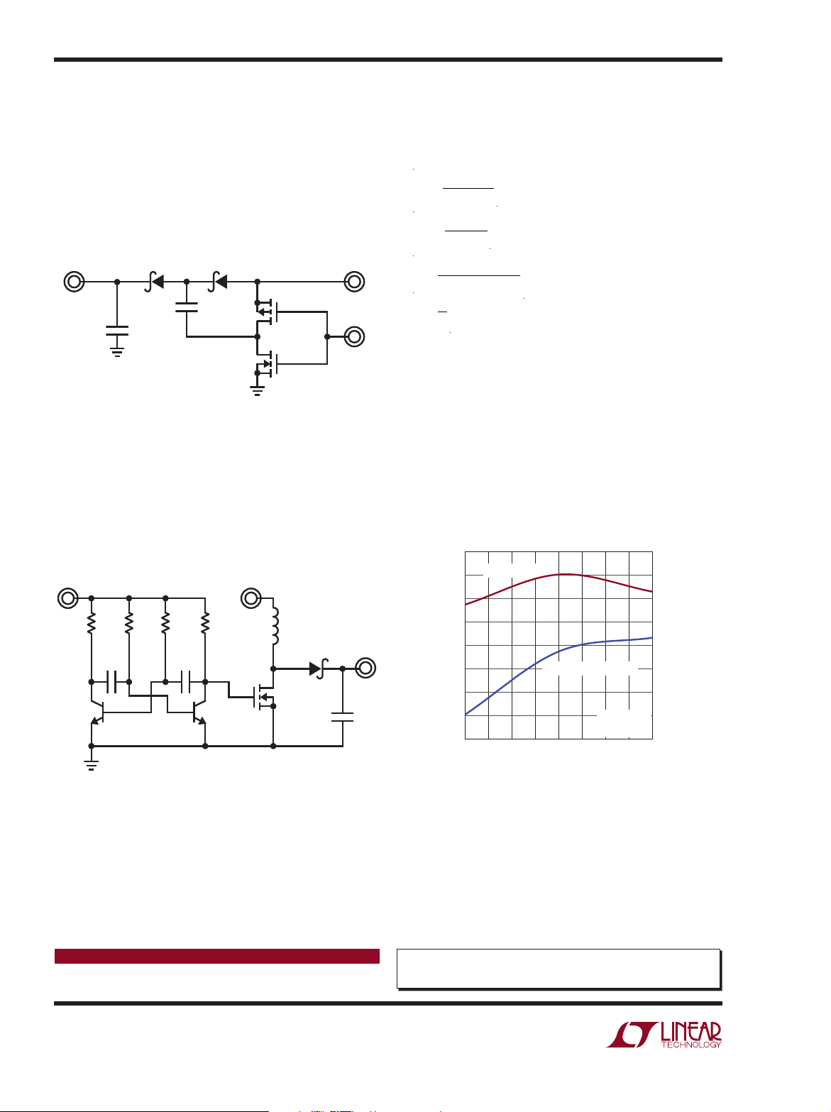
Figure 2 shows a simple, low cost solution for output
−
voltages between 2.5V and 4.7V. This is a voltage doubler scheme based on small P-channel and N-channel
MOSFETs, Q1 and Q2. The gates of these transistors are
controlled by the bottom gate driver, BG of the controller. When BG is high, Q2 is on, Q1 is off and capacitor
C1 charges from output voltage V
through D1. When
OUT
BG is low, Q2 is off, Q1 is on and capacitor C1 delivers
a voltage close to 2 • V
E3
EXTV
CC
Figure 2. Voltage Doubler Allows External Bias
from V
D2
MBR0520D1MBR0520
C2
2.2µF
in the Range of 2.5V to 4.7V
OUT
to EXTVCC.
OUT
C1
2.2µF
Q1
FDN340P
Q2
NDS331N
DN493 F02
E2
V
OUT
E1
BG
Figure 3 shows a solution for voltages below 2.5V. The
circuit consists of an astable multivibrator based on
transistors Q1 and Q2, and a boost based on N-channel
Q3 and inductor L1. Q1 and Q2 are biased from INTV
CC
and output voltage V
EXTV
. The multivibrator frequency is set at 50kHz to
CC
is stepped up to 5V, which feeds
OUT
minimize the EMI signature. The pulse width is defined
by the ratio of resistors R1 and R2, as per the following
expressions:
T •(1
0.7 • C1
T •D
0.7 • C2
EXTV
1
ƒ
CC
D)
− V
CC
OUT
R1=
R2 =
EXTV
D =
T =
Conclusion
The efficiency of high input voltage DC/DC controllers
can be significantly improved by using the controller’s
output voltage to power the IC, instead of allowing the
internal LDO to produce the bias voltage. For input voltages above 30V, efficiency improvements of 2% to 3%
are realized when a voltage doubler circuit is used for a
3.3V at 5A output (see Figure 4). Similar efficiency improvements are shown for a 1.8V at 7A converter with a
multivibrator-based circuit.
INTV
E1
RC1
CC
R1
1k
93.1kR237.4k
C1
220pF
Q1
FMMT2222ATA
C2
220pF
E2
V
OUT
RC2
1k
Q2
FMMT2222ATA
L1
LPS5030-334ML
330µH
D1
MBR0520
Q3
TN0200K
Figure 3. Boost Controlled By Astable Multivibrator
Is Used for V
Data Sheet Download
www.linear.com
Lower Than 2.5V
OUT
DN493 F03
EXTV
C3
2.2µF
92
CHARGE PUMP
91
90
89
88
E3
CC
(%)
87
86
85
84
1
1.5 2 2.5 3 4.5 5
STANDARD SOLUTION
(A)
3.5 4
VIN = 50V
= 3.3V
V
OUT
DN493 F04
Figure 4. LTC3890/LTC3891
Efficiency Improvement
For applications help,
call (408) 432-1900, Ext. 2134
Linear Technology Corporation
dn493f LT/AP 0811 226K • PRINTED IN THE USA
1630 McCarthy Blvd., Milpitas, CA 95035-7417
(408) 432-1900
●
FAX: (408) 434-0507 ● www.linear.com
LINEAR TECHNOLOGY CORPORATION 2011
 Loading...