

Step-Down Converter Delivers 25A at 12V
Design Note 1024
Victor Khasiev
from Inputs Up to 60V
OUT
Introduction
The LTC3890 (dual outputs) and LTC3891 (single
output) step-down DC/DC controllers directly accept
inputs from 4V to 60V. This wide input range covers
input voltages for single or double battery automotive
environments, thus eliminating the need for snubbers
and voltage suppression circuitry typically required to
protect ICs during load dumps. This range also encompasses 4 8V telecom applications. If no gal vanic isolation
is required between the input and output voltages, the
LTC3890 and LTC3891 can replace ex pensive and bulky
transformer-based converters. When compared to a
transformer-based solution, an LTC3890 or LTC3891
step-down converter increases efficiency, reduces
power loss in the supply lines, simplifies layout and
significantly reduces the bill of materials.
PLLIN
FREQ
RUN1
RUN2
SS1
SS2
ITH1
ITH2
V
FB1
V
FB2
PGND
PGOOD1
PGOOD2
ILIM
EXTV
LTC3890
CC
VIN, 16V TO 60V
V
IN
–
SENSE1
+
SENSE1
TG1
SW1
BOOST1
BG1
INTV
CC
TG2
SW2
BOOST2
BG2
+
SENSE2
–
SENSE2
1µF/100V
2.2Ω
22
1
2.2pF
32
26
25
DFLS1100
0.1µF
1
23
INT
19
15
16
DFLS1100
0.1µF
17
18
100Ω
10
2.2pF
9
1M
5
30.1k
57.6k
0.1µF
47pF
4.7nF
9.76k
47pF
35.7k
V
OUT
499k
10pF
1µF
2
7
8
29
13
30
12
31
11
21
27
14
28
20
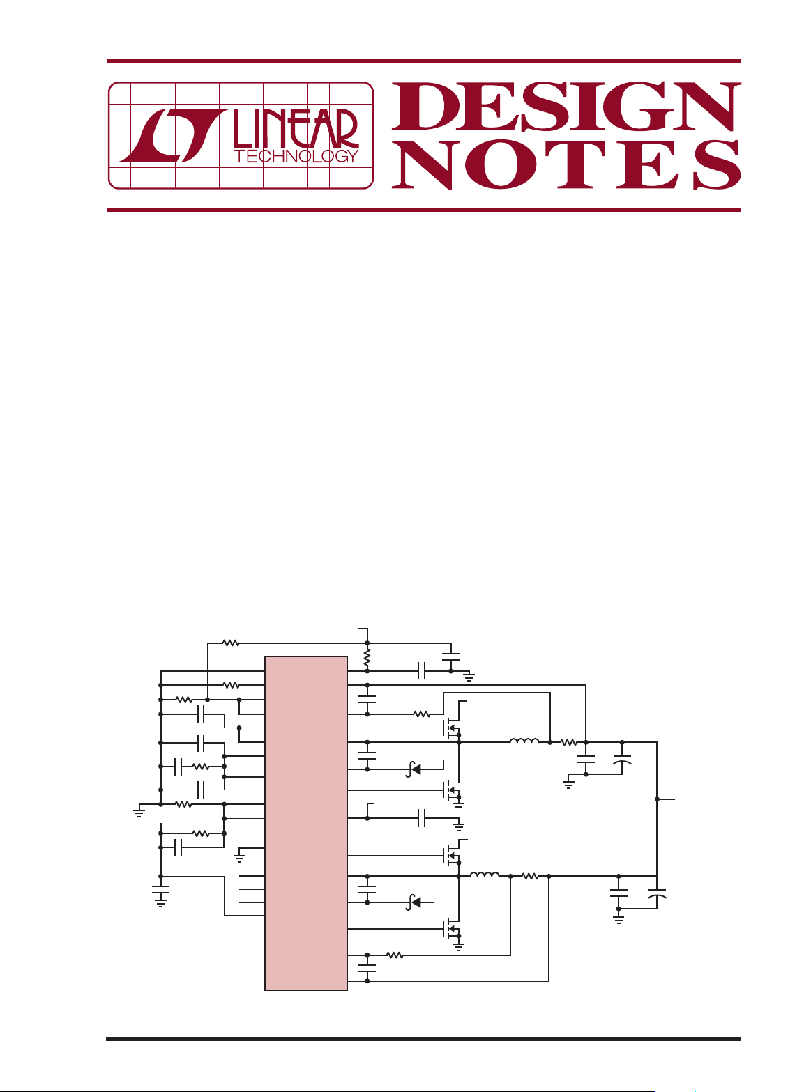
High Efficiency 2-Phase Converter Produces 12V
at 25A
Figure 1 shows the LTC3890 in a 2-phase single output
step-down converter configuration that delivers 25A
at 12V, which can be scaled up to 75A by adding more
LTC3890 ICs to increase the number of power phases.
For lower output current, the single-phase LTC3891
can be used. Implementing a 2-phase converter simply
requires tying together the independent channel pins
of the LTC3890, namely, FB1 and FB2, TRACK/SS1 and
TRACK/SS2, RUN1 and RUN2, ITH1 and ITH2.
Although the ITH pins are connected together, each is
terminated to a separate 47pF capacitor to compensate
L, LT, LTC, LTM, Linear Technology, the Linear logo and Burst Mode are registered
trademarks of Linear Technology Corporation. All other trademarks are the property
of their respective owners.
2.2µF/100V
×4
V
INT
INT
IN
RJK0651DPB
RJK0653DPB
V
IN
RJK0651DPB
L2 10µH
RJK0653DPB
L1
10µH
3m
+
10µF
150µF
×2
V
OUT
12V AT 25A
3m
+
10µF
150µF
×2
L1, L2: WÜRTH 7443631000
DN1024 F01
100Ω
4.7µF
Figure 1. High Efficiency Converter Produces 25A at 12V
OUT
from Inputs Up to 60V
for possible noise from interconnecting traces. A
2
relatively low switching frequency, around 150kHz,
and a relatively high phase inductance of 10µH are
used to reduce switching losses at high input voltages.
The output voltage is fed to the EXTV
pin to reduce
CC
losses associated with biasing the chip and internal
gate drivers at high input voltages.
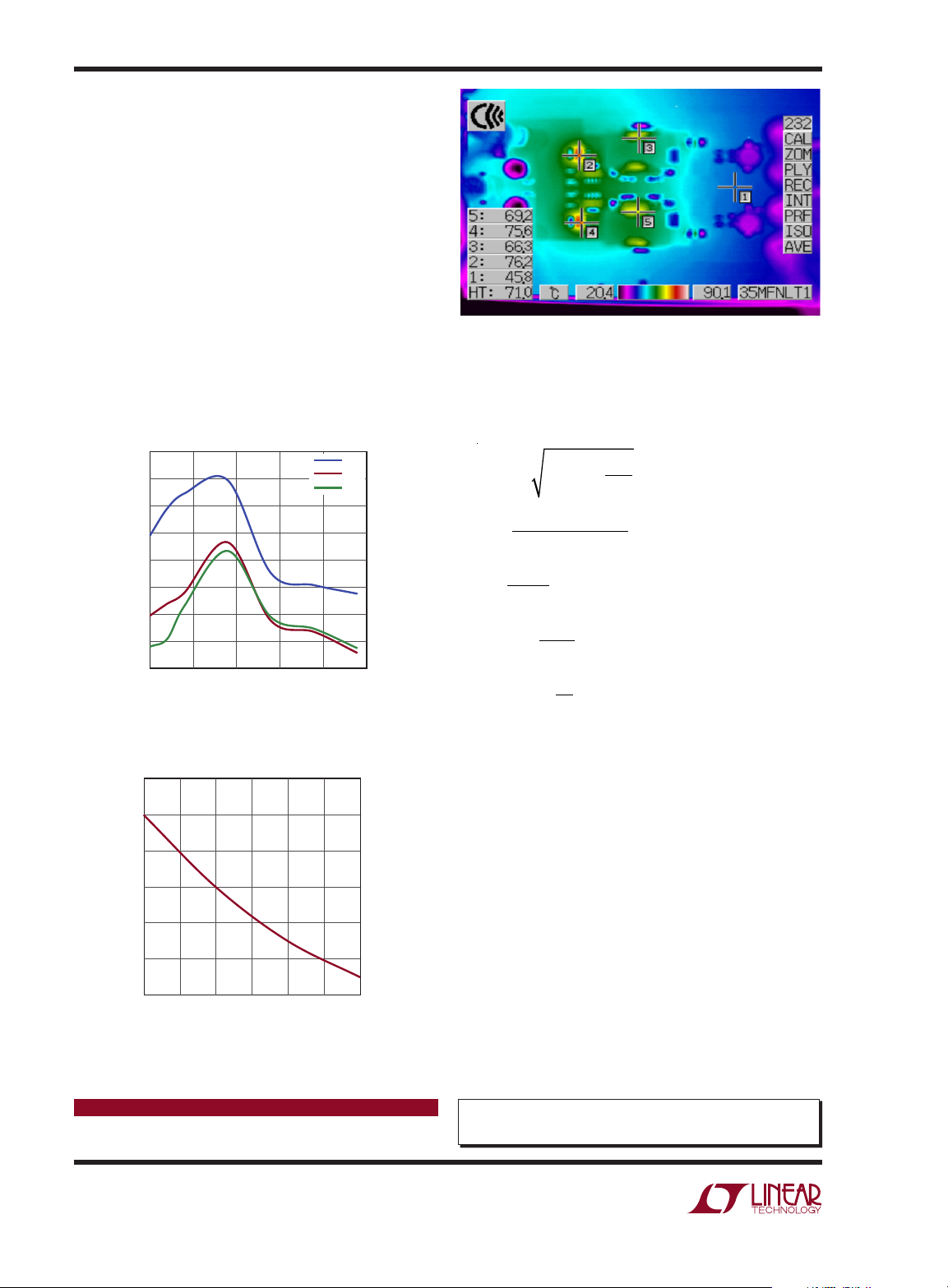
Circuit Performance
Efficiency is shown in Figure 2, measured without
cooling air flow. Efficiency peaks close to 98% in the
middle of the load range and declines to 96% at the
25A maximum load. Figure 3 shows the average input
current vs input voltage at no load in Burst Mode
®
operation. The v alue of this current is below 0.5mA. Figure
4 shows a thermal map of the board with no air flow
present at V
EFFICIENCY (%)
Figure 2. Efficiency at VIN = 20V, 36V and 50V
0.22
0.20
0.18
0.16
0.14
INPUT CURRENT (mA)
0.12
0.10
Figure 3. Average Input Current vs Input Voltage at
No Load. V
IN
99.0
98.5
98.0
97.5
97.0
96.5
96.0
95.5
95.0
OUT
= 20V and V
OUT
1161 16 21 26
LOAD (A)
302520 35 40 45 50
V
IN
is 12V.
= 12V at 25A (300W).
20V
36V
50V
DN1024 F02
DN1024 F03
Figure 4. Temperature Hot Spots with No Air Flow
Component Selection
Two values define selection of the inductor: RMS current (I
) and saturation current (IPK):
RMS
2
OUT
∆I
12
)•D
I
RMS
∆I=
= (IPH)2+
(V
– V
IN
L • f
V
OUT
D =
V
IN
I
IPH= k •
OUT
2
IPK=IPH+
∆I
where f is the switching frequency and k is a coefficient
defined by the current imbalance between the phases.
For converters based on the LTC3890, k = 1.08, assuming current sense resistors with a 1% tolerance.
Selection of power MOSFETs and input/output capacitors is described in detail in the LTC3890 data sheet.
It is important to note that the typical internal V
CC
voltage and, consequently, the MOSFET gate voltage
is 5.1V. This means that logic level MOSFETs must be
used in the design.
Conclusion
The LTC3890 dual output, synchronous step-down
converter can be easily configured as a single output,
dual phase conver ter for high input voltage, high output
current automotive and telecom applications.
Data Sheet Download
www.linear.com
Linear Technology Corporation
1630 McCarthy Blvd., Milpitas, CA 95035-7417
(408) 432-1900
●
FAX: (408) 434-0507 ● www.linear.com
For applications help,
call (408) 432-1900, Ext. 3161
dn1024 LT 0212 • PRINTED IN THE USA
LINEAR TECHNOLOGY CORPORATION 2012
 Loading...