

L DESIGN FEATURES
V
OUT
(AC)
50mV/DIV
V
SW
20V/DIV
I
L
10A/DIV
I
LOAD
10A/DIV
5µs/DIV
LOAD STEP 0A TO 10A
VIN = 12V
V
OUT
= 1.2V
MODE = 0V
SW FREQ = 400kHz
V
OUT
(AC)
50mV/DIV
V
SW
20V/DIV
I
L
10A/DIV
I
LOAD
10A/DIV
5µs/DIV
LOAD STEP 10A TO 0A
VIN = 12V
V
OUT
= 1.2V
MODE = 0V
SW FREQ = 400kHz
Compact No R
SENSE
Controllers
Feature Fast Transient Response
and Regulate to Low V
from Wide Ranging V
Introduction
The trend in digital electronics is to
lower voltages and increasing load currents. This puts pressure on DC/DC
converters to produce low voltages
from increasingly voltage-variable
supplies, such as stacked batteries
and unregulated intermediate power
buses, so power converters must be
optimized for low output voltages, low
duty factors, and wide control bandwidths. To meet these requirements,
the DC/DC controller IC must offer
high voltage accuracy, good line and
load regulation, and fast transient
response. The constant on-time valley current mode architecture used in
the LTC3878 and LTC3879 is ideally
suited to low duty factor operation,
offering a compact solution with excellent system performance.
The LTC3878 and LTC3879 are
a new generation of No R
controllers that meet the demanding
requirements of low voltage supplies
for digital electronics. The LTC3878 is
a pin compatible replacement for the
LTC1778 in designs where EXTVCC
is not required. The LTC3879 adds
separate RUN and TRACK/SS pins for
applications requiring voltage tracking. Both devices offer continuously
programmable current limit, using
the bottom MOSFET VDS voltage to
sense current.
Valley Current Mode
Control Simplifies Loop
Compensation…
There are two common implementations of current mode control. Peak
current mode control regulates the
high side MOSFET on-time, while
valley current mode regulates the
bottom side MOSFET off-time. The
current mode loop bandwidth is in-
18
SENSE
™
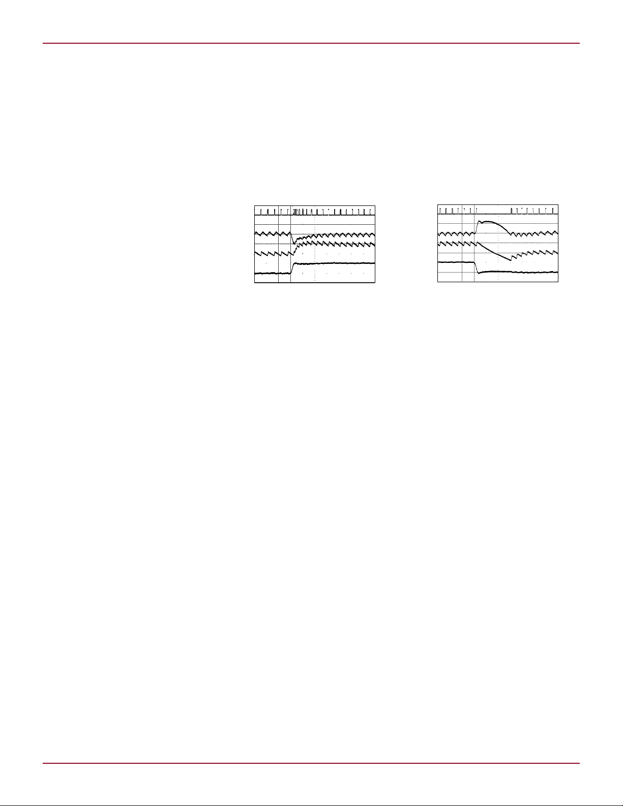
Figure 1. Transient response,
positive load step
versely proportional to the on-time for
a peak current controller and inversely
proportional to the off-time for a valley
mode controller. A peak current mode
controller with an on-time of 50ns
must have a closed current loop bandwidth exceeding 20MHz. For a valley
current mode controller, the current
loop bandwidth is determined by the
typical off-time of 220ns, resulting in a
closed current loop bandwidth requirement of only 4.5MHz. Consequently,
valley current mode control has less
stringent bandwidth requirements for
the same system performance when
compared to a peak current mode
control in a similar application. This
allows the LTC3878 and LTC3879 to
offer high performance, low duty factor
operation at reasonable current loop
bandwidths.
The constant on-time valley current
mode control of the LTC3878 and
LTC3879 simplifies compensation
design by eliminating the need for
slope compensation. A fixed frequency
valley mode controller requires slope
compensation when operating at less
than 50% duty factor to prevent subcycle oscillation. Subcycle oscillation
occurs because the PWM pulse width
IN
OUT
by Terry J. Groom
Figure 2. Transient response,
load release
is not uniquely determined by inductor
current alone. This oscillation cannot
exist in constant-on-time control because the PWM pulse width is uniquely
determined by the internal open loop
pulse generator. True current mode
control and constant on-time combine
to give the LTC3878 and LTC3879
performance advantages over other
constant on-time regulators or fixed
frequency valley current mode control
architectures.
…and Improves Transient
Response Time
In a buck controller, transient response
is largely determined by how quickly
the inductor current responds to loop
disturbances. The most demanding
loop disturbances are load steps and
load releases.
The inherent speed advantage of
a constant on-time architecture lies
in the fact that the regulator is pulse
frequency modulated (PFM) insead
of pulse width modulated (PWM).
Although the switching frequency is
fixed in steady state operation, it can
increase or decrease as required in
response to an output load step or
load release.
Linear Technology Magazine • June 2009
DESIGN FEATURES L
f Hz
MAX
ON OFF MIN
t t
=
(
)
+
1
( )
( )
f g EA R
I
C
V
V
CGO m C
LIMIT
OUT
REF
OUT
= • •( )
.1 6
1
I
L
5A/DIV
V
OUT
0.5V/DIV
TRACK/SS
0.5V/DIV
20ms/DIV
VIN = 12V
V
OUT
= 1.2V
SW FREQ = 400kHz
+
TRACK/SS
LTC3879
BOOST
16
C
B
0.22µF
M1
RJK0305DPB
C
VCC
4.7µF
C
C1
220pF
C
C2
33pF
D
B
CMDSH-3
L1
0.56µH
C
OUT1
330µF
2.5V
s2
C
OUT2
47µF
6.3V
s2
+
C
IN1
10µF
50V
s3
C
IN2
100µF
50V
V
OUT
1.2V
15A
V
IN
4.5V TO 28V
1
PGOOD
R
PG
100k
R2
80.6k
R
C
27k
R
FB1
10.0k
R1
10.0k
TG
152
V
RNG
SW
143
MODE PGND
134
I
TH
BG
125
SGND INV
CC
116
I
ON
V
IN
107
V
FB
RUN
98
R
ON
432k
R
FB2
10.0k
M2
RJK0330DPB
C
IN1
: UMK325BJ106MM s3
C
OUT1
: SANYO 2R5TPE330M9 s2
C
OUT2
: MURATA GRM31CR60J476M s2
L1: VISHAY IHLP4040DZ-11 0.56µH
C
SS
0.1µF
LOAD CURRENT (A)
30
EFFICIENCY (%)
90
100
20
10
80
50
70
60
40
0.01 1 10 100
0
0.1
CONTINUOUS
MODE
DISCONTINUOUS
MODE
VIN = 12V
V
OUT
= 1.2V
SW FREQ = 400kHz
The maximum frequency in response to a load step is determined
by the on-time plus the off-time:
In low duty factor applications the
maximum frequency is typically much
greater than the nominal operating frequency, producing excellent transient
characteristics.
Figure 1 shows the load step response of a 12V-to-1.2V converter
operating at 400kHz. In this case the
on-time is equal to 250ns and the
minimum off-time is 220ns. The maximum frequency available to respond
to a load step is 2.12MHz, which is
over five times the nominal switching
frequency. Note the increase in switching frequency of the VSW waveform
in response to the 10A load step. The
increase in switching frequency causes
the inductor current to ramp faster in
constant on-time PFM controllers than
is possible in a true fixed frequency
PWM.
In response to a load release
(Figure 2), the minimum frequency
is effectively zero, since the bottom
gate is held high as long as needed
to ramp the inductor current down
to the internal regulation set point.
In this example, the inductor current ramps from 11A to –8A in 13µs
as the output recovers from the load
step. For both load transient cases,
variable frequency has an inherent
speed advantage over fixed frequency
in transient recovery.
Start-Up Options
The LTC3878 offers the simplicity of
current limited start-up through the
combined RUN/SS pin. When RUN/SS
is greater than 0.7V all internal bias is
activated. Once RUN/SS exceeds 1.5V,
switching begins. The current limit is
gradually increased as the RUN/SS
pin voltage ramps until reaching full
Figure 3. Start-up into a prebiased output
Transient settling requires both
the large signal ramping of inductor current and the stable settling of
the output to the desired regulation
point. Excessive output overshoot or
ringing indicates marginal system
stability likely caused by inadequate
compensation. A rough compensation
check can be made by calculating the
gain crossover frequency, given by the
following equation (where V
for the LTC3878 and V
REF
= 0.8V
REF
= 0.6V for
the LTC3879):
As a rule of thumb, the gain crossover frequency should be less than
20% of the switching frequency. With
any analog system, transient response
is determined by closed loop bandwidth. In order to optimize for transient
performance, it is desirable to have a
small inductor and a wide closed loop
bandwidth. A small inductor is desired
for quick output current response,
while the closed loop bandwidth and
phase margin determines how quickly
the output settles after a load step.
output at approximately 3V.
separate RUN and TRACK/SS pins. All
internal bias is activated when RUN
exceeds 0.7V. Switching begins when
RUN exceeds 1.5V. The TRACK/SS
pin can also be used for input voltage tracking, where the LTC3879’s
output tracks the voltage on the
TRACK/SS pin until it exceeds 0.6V.
Once TRACK/SS exceeds 0.6V the
output regulates to the internal 0.6V
reference. An internal 1µA pull-up current is available to create a soft-start
voltage ramp when a small capacitor
is connected to TRACK/SS. Together,
RUN and TRACK/SS enable a number
Figure 4. Efficiency for application in Figure 5
The LTC3879 adds the flexibility of
Linear Technology Magazine • June 2009
Figure 5. Wide input range to 1.2V at 15A, operating at 400kHz
19

L DESIGN FEATURES
+
TRACK/SS
V
MASTER
LTC3879
BOOST
16
C
B
0.22µF
M1
RJK0305DPB
C
VCC
4.7µF
C
C1
330pF
C
C2
47pF
D
B
CMDSH-3
L1
0.44µH
C
OUT1
330µF
2.5V
s3
C
OUT2
100µF
6.3V
s2
+
C
IN1
10µF
16V
s2
C
IN2
180µF
16V
V
OUT
1.2V
20A
V
IN
4.5V TO 14V
1
PGOOD
R
PG
100k
R2
57.6k
R
TR2
10.0k
R
C
15k
R
FB1
10.0k
R1
10.0k
R
TR1
10.0k
TG
152
V
RNG
SW
143
MODE PGND
134
I
TH
BG
125
SGND INV
CC
116
I
ON
V
IN
107
V
FB
RUN
98
R
ON
576k
R
FB2
10.0k
C
PL
470pF
C
F
0.1µF
R
F
1Ω
M2
RJK0330DPB
C
IN1
: TDK C3225X5R1C106MT s2
C
OUT1
: SANYO 2R5TPE330M9 s3
C
OUT2
: MURATA GRM31CR60J107ME39 s2
L1: PULSE PA0513.441NLT
5ms/DIV
VIN = 12V
V
OUT
= 1.2V
SW FREQ = 400kHz
V
MASTER
0.5V/DIV
V
OUT
0.5V/DIV
Figure 6. Coincident tracking example produces 1.2V at 20A, operating at 300kHz
of start-up supply sequencing and
tracking options.
Both the LTC3878 and LTC3879
have the ability to start up onto prebiased outputs. Because current limit
is ramped in the LTC3878, prebiased
output voltages are not an issue. The
LTC3879 output tracks the input on
the TRACK/SS pin. To accommodate
prebiased outputs, the LTC3879 will
not switch until the TRACK/SS pin
exceeds the VFB voltage. Once TRACK/
SS exceeds VFB the output follows the
TRACK/SS pin in continuous conduction mode until the output regulates
to the internal reference.
In Figure 3 the LTC3879 output
is prebiased to 0.5V. The TRACK/SS
pin ramps from zero and crosses the
prebiased output feedback point at
approximately 28ms, when switching
begins. Once switching begins the output enjoys a smooth soft-start ramp.
The LTC3879 operates in continuous
conduction mode during start-up, regardless of the mode setting, allowing
regulation of the output voltage to the
TRACK/SS input pin voltage during
soft-start.
High Efficiency
The LTC3879 and LTC3879 offer
excellent efficiency through the combination of strong gate drivers and short
dead time. The top gate driver offers
a 2.5Ω pull up resistance and a 1.2Ω
pull down, while the bottom gate driver
offers a 2.5Ω pull up and a 0.7Ω pull
20
down. Dead time has been measured
as low as 12ns, minimizing switching
loss. Efficiency has been measured at
91.8% in a 1.2V/20A application.
The LTC3878 and LTC3879 offer
both discontinuous conduction mode
(DCM) and continuous conduction
mode (CCM) operation. Figure 4 shows
peak efficiency over 90% for 12V and
15A in CCM. In CCM, either the top
MOSFET or the bottom MOSFET is
active and the output inductor is
continuously conducting. In DCM,
the top and bottom MOSFET can be
off simultaneously in order to improve
low current efficiency. In Figure 4, at
100mA, the efficiency is greater than
70% in DCM, compared to only 20%
in CCM. Improvements in efficiency in
DCM are seen when the load is less
than the DC average of the steady state
ripple current, causing the regulator to
enter discontinuous conduction.
Application Example:
4.5V-to-28V In to 1.2V Out
with 90% Peak Efficiency
Figure 5 shows an application that
converts a wide 4.5V-to-28V input
voltage to a 1.2V ±5% output at 15A.
The nominal ripple current is chosen to
be 35% resulting in a 0.55µH inductor
and ripple current of 5.1A. Because the
top MOSFET is on for a short time, an
RJF0305DPB (R
nal), C
MILLER
= 150pF, V
sufficient. The stronger RJK0330DPB
is chosen for the bottom MOSFET, with
= 10mΩ (nomi-
DS(ON)
MILLER
= 3V) is
a typical R
of 3.8mΩ. This results
DS(ON)
in 90% peak efficiency. Note that the
efficiency, transient and start-up
waveforms in Figures 1–4 were taken
from this design example.
Tracking
Figure 6 shows a LTC3879 in a
1.2V/20A output, 300kHz application
design with coincident rail tracking. In
coincident tracking, two supplies ramp
up in unison until the lower voltage
supply reaches regulation, at which
point the higher voltage supply continues to ramp to its regulated value.
Coincident tracking is implemented by
making the resistor divider from the
master voltage to the TRACK/SS pin
equal to the feedback divider from V
to VFB. In Figure 6, the output is 1.2V,
so the divider is equal to 0.6V/1.2V,
or 0.5. This design tracks any master
supply that is equal to or greater than
1.2V. The TRACK/SS pin should be
greater than 0.65V in regulation to
ensure that the LTC3879 has sufficient
Figure 7. Coincident tracking waveforms
for application in Figure 6
Linear Technology Magazine • June 2009
OUT

DESIGN FEATURES L
t
t
t
V
IN
18V TO 72V
GND
5V, 2A
+V
OUT
–V
OUT
PA1277NL
T1
162k
1k
6.81k
10pF
2200pF
1µF
330pF
22.1k
M1
Si4848DY
LT4430ES6
0.47µF
PS2801-1
UPS840
C
OUT
100µF
×2
BAT54C
BAS516
C
IN
1µF
×2
4.7nF
10k
51.1Ω
BAV21W
BAS516
6.81k
0.04Ω
105k
4.7µF
0.1µF
INTVCC
GATE
SENSE
SYNC
GND
V
IN
LT3758
V
IN
SS
VC
SHDN/UVLO
FBX
RT
8.66k 36.5k
100pF
OPTO
COMP
FB
V
IN
GND
OC
margin to switch from tracking the
TRACK/SS input voltage to regulating
to the internal reference.
Figure 7 shows typical tracking
waveforms of the application in Figure 6. V
voltage, V
and the reference supply
OUT
MASTER
, are equal and track
together during start-up until they
reach 1.2V, at which point V
lates to 1.2V while V
MASTER
regu-
OUT
continues
ramping to 1.8V.
Conclusion
The LTC3878 and the LTC3879 support a VIN range from 4V to 38V (40V
abs max). The regulated output voltage
is programmable from 90% VIN down to
LT3757/58, continued from page 4
An 18V–72V Input,
5V/2A Output Isolated
Flyback Converter
The basic design shown in Figure 7
can be modified to provide DC isolation between the input and output
with the addition of a reference, such
as the LT4430, on the secondary side
of the transformer and an optocoupler
0.8V (for the LTC 3878) and 0.6V (for
the LTC3879). The output regulation
accuracy is ±1% over the full –40°C to
85°C temperature range. The operating
frequency is resistor programmable
and is compensated for variations in
VIN. Current limit is continuously programmable and is measured without
a sense resistor by using the voltage
drop across the external synchronous
bottom MOSFET.
The valley current mode architecture is ideal for low duty factor
operation and allows very low output
voltages at reasonable current loop
bandwidths. Compensation is easy
to design and offers robust and stable
to provide feedback from the isolated
secondary to the LT3758. Figure 8
shows an 18V–72V input, 5V/2A output isolated flyback converter.
Conclusion
The LT3757 and LT3758 are versatile
control ICs optimized for a wide variety
of single-ended DC/DC converter to-
operation even with low ESR ceramic
output capacitors. The LTC3878 offers current limited start-up, while
the LTC3879 has separate run and
output voltage tracking pins. The
LTC3878 is available in the GN16
package, and the LTC3879 is available in thermally enhanced MSE16
and QFN (3mm × 3mm) packages.
Excellent performance and compact
size make the LTC3878 and LTC3879
well suited to small, tightly constrained
applications such as distributed power
supplies, embedded computing and
point of load applications.
L
pologies. Both offer a particularly wide
input voltage range. These ICs produce
space saving, cost efficient and high
performance solutions in any of these
topologies. The range of applications
extends from single-cell, lithiumion powered systems to automotive,
industrial and telecommunications
power supplies. L
Linear Technology Magazine • June 2009
Figure 8. 18V–72V input, 5V/2A isolated flyback converter
21
 Loading...