

LTC3862
Multi-Phase Current Mode
Step-Up DC/DC Controller
FEATURES
n
Wide VIN Range: 4V to 36V Operation
n
2-Phase Operation Reduces Input and Output
Capacitance
n
Fixed Frequency, Peak Current Mode Control
n
5V Gate Drive for Logic-Level MOSFETs
n
Adjustable Slope Compensation Gain
n
Adjustable Max Duty Cycle (Up to 96%)
n
Adjustable Leading Edge Blanking
n
±1% Internal Voltage Reference
n
Programmable Operating Frequency with One
External Resistor (75kHz to 500kHz)
n
Phase-Lockable Fixed Frequency 50kHz to 650kHz
n
SYNC Input and CLKOUT for 2-, 3-, 4-, 6- or
12-Phase Operation (PHASEMODE Programmable)
n
Internal 5V LDO Regulator
n
24-Lead Narrow SSOP Package
n
5mm × 5mm QFN with 0.65mm Lead Pitch and
24-Lead Thermally Enhanced TSSOP Packages
APPLICATIONS
n
Automotive, Telecom and Industrial Power Supplies
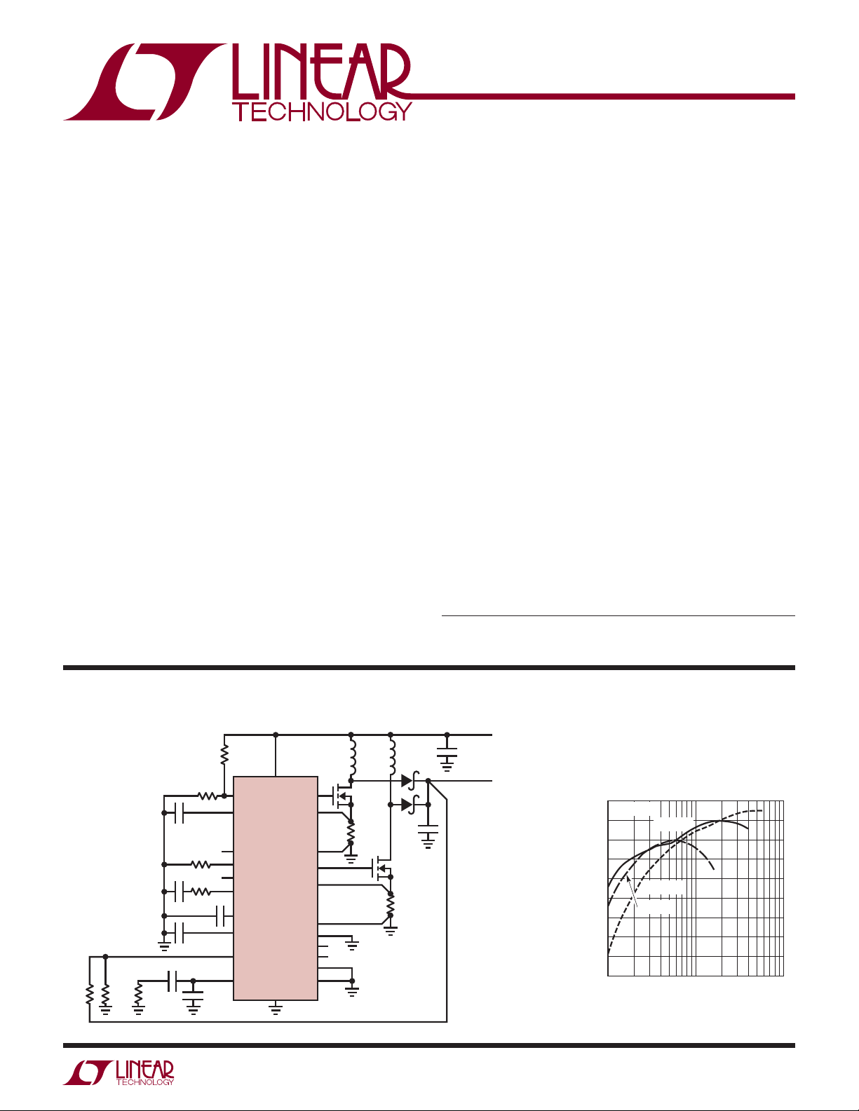
DESCRIPTION
The LTC®3862 is a two phase constant frequency, current
mode boost and SEPIC controller that drives N-channel
power MOSFETs. Two phase operation reduces system
fi ltering capacitance and inductance requirements. The 5V
gate drive is optimized for most automotive and industrial
grade power MOSFETs.
Adjustable slope compensation gain allows the user to fi netune the current loop gain, improving noise immunity.
The operating frequency can be set with an external resistor
over a 75kHz to 500kHz range and can be synchronized
to an external clock using the internal PLL. Multi-phase
operation is possible using the SYNC input, the CLKOUT
output and the PHASEMODE control pin allowing 2-, 3-,
4-, 6- or 12-phase operation.
Other features include an internal 5V LDO with undervoltage
lockout protection for the gate drivers, a precision RUN
pin threshold with programmable hysteresis, soft-start
and programmable leading edge blanking and maximum
duty cycle
L, LT, LTC and LTM are registered trademarks of Linear Technology Corporation.
All other trademarks are the property of their respective owners. Protected by U.S. Patents,
including 6144194, 6498466, 6611131.
TYPICAL APPLICATION
84.5k
RUN
INTV
CC
BLANK
FREQ
SYNC
PLLFLTR
SS
3V8
FB
ITH
V
IN
LTC3862
PHASEMODE
SGND
475k 12.4k
68.1k
4.7µF
10nF
10nF
24.9k
66.5k
10k
10nF
1nF
100pF
GATE1
SENSE1
SENSE1
GATE2
SENSE2
SENSE2
PGND
CLKOUT
SLOPE
D
MAX
V
IN
5V TO 36V
19.4µH 19.4µH
+
220µF
0.006
–
+
–
50V
0.006
22µF
50V
3862 TA01
V
OUT
48V
5A (MAX)
Effi ciency vs Output Current
98
V
= 48V
OUT
96
94
92
90
88
EFFICIENCY (%)
86
84
82
80
100
VIN = 12V
VIN = 24V
VIN = 5V
1000 10000
LOAD CURRENT (mA)
3862 TA01b
3862fa
1
LTC3862
ABSOLUTE MAXIMUM RATINGS
(Notes 1, 2)
Input Supply Voltage (VIN) ......................... –0.3V to 40V
INTV
INTV
Voltage ............................................ –0.3V to 6V
CC
LDO RMS Output Current .........................50mA
CC
RUN Voltage ................................................ –0.3V to 8V
SYNC Voltage ............................................... –0.3V to 6V
SLOPE, PHASEMODE, D
MAX
,
BLANK Voltage ........................................... –0.3V to 3V8
+
SENSE1
SENSE2
, SENSE1–, SENSE2+,
–
Voltage ....................................... –0.3V to 3V8
SS, PLLFLTR Voltage ................................. –0.3V to 3V8
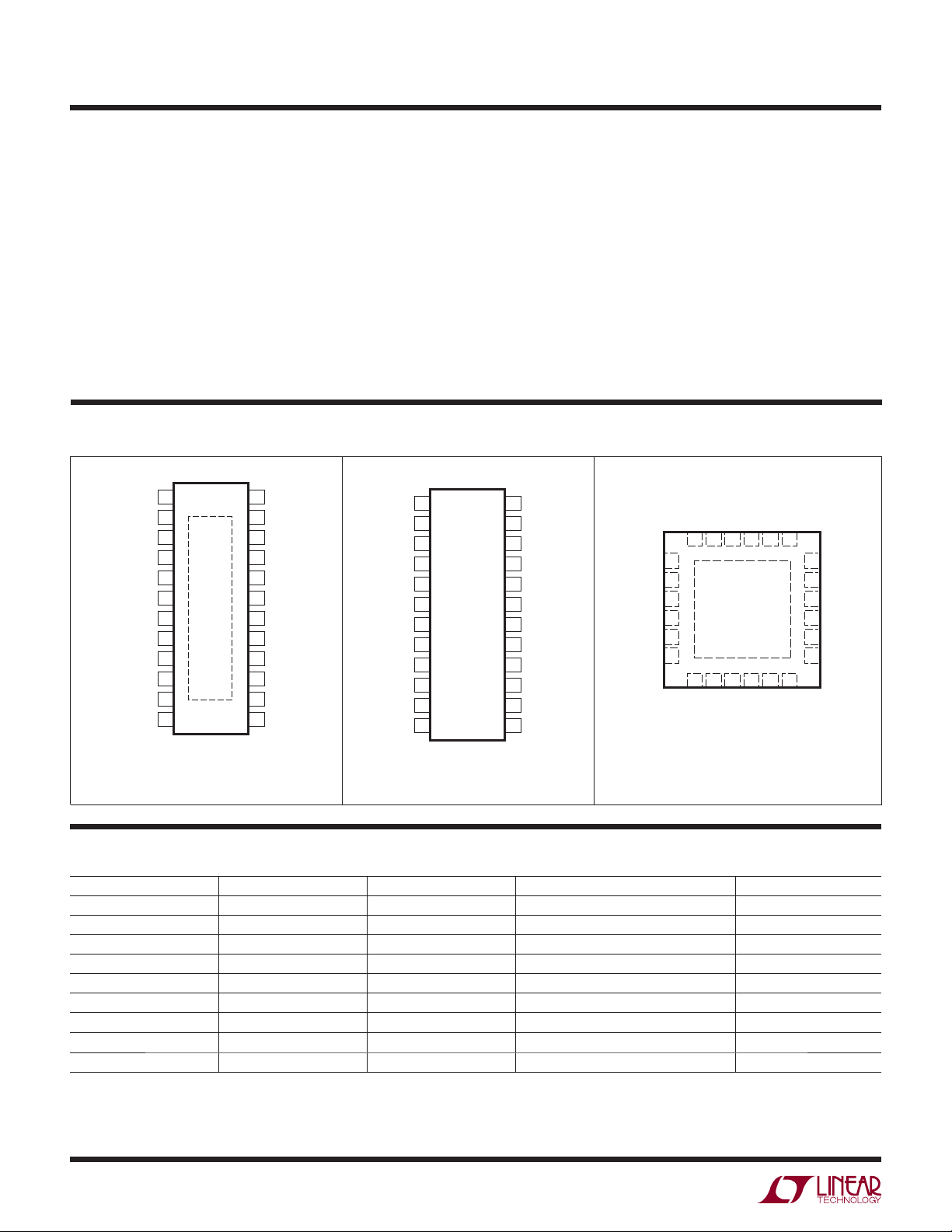
PIN CONFIGURATION
TOP VIEW
1
D
MAX
2
SLOPE
3
BLANK
PHASEMODE
CLKOUT
PLLFLTR
EXPOSED PAD (PIN 25) IS PGND, MUST BE SOLDERED TO PCB
4
5
FREQ
6
SS
7
ITH
8
FB
9
SGND
10
11
SYNC
12
FE PACKAGE
24-LEAD PLASTIC TSSOP
T
= 150°C, θJA = 38°C/W
JMAX
25
24
23
22
21
20
19
18
17
16
15
14
13
3V8
SENSE1
SENSE1
RUN
V
IN
INTV
CC
GATE1
PGND
GATE2
NC
SENSE2
SENSE2
+
–
–
+
D
MAX
SLOPE
BLANK
PHASEMODE
FREQ
SS
ITH
FB
SGND
CLKOUT
SYNC
PLLFLTR
24-LEAD NARROW PLASTIC SSOP
TOP VIEW
1
2
3
4
5
6
7
8
9
10
11
12
GN PACKAGE
T
= 150°C, θJA = 85°C/W
JMAX
ITH Voltage ............................................... –0.3V to 2.7V
FB Voltage .................................................. –0.3V to 3V8
FREQ Voltage ............................................ –0.3V to 1.5V
Operating Junction Temperature Range (Notes 3, 4)
LTC3862E ............................................. –40°C to 85°C
LTC3862I............................................ –40°C to 125°C
LTC3862H .......................................... –40°C to 150°C
Storage Temperature Range ................... –65°C to 150°C
Refl ow Peak Body Temperature ........................... 260°C
TOP VIEW
3V8
24
23
22
21
20
19
18
17
16
15
14
13
SENSE1
SENSE1
RUN
V
IN
INTV
CC
GATE1
PGND
GATE2
NC
SENSE2
SENSE2
+
–
PHASEMODE
FREQ
SS
ITH
FB
–
+
EXPOSED PAD (PIN 25) IS PGND, MUST BE SOLDERED TO PCB
SLOPE
DMAX
3V8
SENSE1+SENSE1–RUN
24 23 22 21 20 19
1
2
3
4
5
6
24-LEAD (5mm s 5mm) PLASTIC QFN
T
JMAX
25
7 8 9
SGND
10 11 12
SYNC
CLKOUT
PLLFLTR
UH PACKAGE
= 150°C, θJA = 34°C/W
+
SENSE2
18BLANK
17
16
15
14
13
–
SENSE2
V
IN
INTV
GATE1
PGND
GATE2
NC
CC
ORDER INFORMATION
LEAD FREE FINISH TAPE AND REEL PART MARKING* PACKAGE DESCRIPTION TEMPERATURE RANGE
LTC3862EFE#PBF LTC3862EFE#TRPBF 3862FE 24-Lead Plastic TSSOP –40°C to 85°C
LTC3862IFE#PBF LTC3862IFE#TRPBF 3862FE 24-Lead Plastic TSSOP –40°C to 125°C
LTC3862HFE#PBF LTC3862HFE#TRPBF 3862FE 24-Lead Plastic TSSOP –40°C to 150°C
LTC3862EGN#PBF LTC3862EGN#TRPBF LTC3862GN 24-Lead Plastic SSOP –40°C to 85°C
LTC3862IGN#PBF LTC3862IGN#TRPBF LTC3862GN 24-Lead Plastic SSOP –40°C to 125°C
LTC3862HGN#PBF LTC3862HGN#TRPBF LTC3862GN 24-Lead Plastic SSOP –40°C to 150°C
LTC3862EUH#PBF LTC3862EUH#TRPBF 3862
LTC3862IUH#PBF LTC3862IUH#TRPBF 3862
LTC3862HUH#PBF LTC3862HUH#TRPBF 3862
24-Lead (5mm × 5mm) Plastic QFN
24-Lead (5mm × 5mm) Plastic QFN
24-Lead (5mm × 5mm) Plastic QFN
–40°C to 85°C
–40°C to 125°C
–40°C to 150°C
Consult LTC Marketing for parts specifi ed with wider operating temperature ranges. *The temperature grade is identifi ed by a label on the shipping container.
Consult LTC Marketing for information on non-standard lead based fi nish parts.
For more information on lead free part marking, go to:
For more information on tape and reel specifi cations, go to: http://www.linear.com/tapeandreel/
http://www.linear.com/leadfree/
3862fa
2
LTC3862
ELECTRICAL CHARACTERISTICS
(Notes 2, 3) The l denotes the specifi cations which apply over the full
operating junction temperature range, otherwise specifi cations are at T
otherwise noted.
SYMBOL PARAMETER CONDITIONS MIN TYP MAX UNITS
Supply Input and INTV
V
IN
I
VIN
INTV
CC
dV
INTVCC(LINE)
dV
INTVCC(LOAD)
V
UVLO
3V8 LDO Regulator Output Voltage 3.8 V
Switcher Control Loop
V
FB
dV
/dV
FB
IN
dV
/dV
FB
ITH
g
m
f
0dB
V
ITH
I
ITH
I
FB
V
ITH(PSKIP)
I
SENSE(ON)
V
SENSE(MAX)
RUN/Soft-Start
I
RUN
V
RUN
V
RUNHYS
I
SS
R
SS
Oscillator
f
OSC
V
FREQ
f
SYNC
V
SYNC
Linear Regulator
CC
VIN Supply Voltage Range 4 36 V
VIN Supply Current
Normal Mode, No Switching
Shutdown
(Note 5)
V
= 0V
RUN
LDO Regulator Output Voltage 4.8 5.0 5.2 V
Line Regulation 6V < VIN < 36V 0.002 0.02 %/V
Load Regulation Load = 0mA to 20mA –2 %
INTVCC UVLO Voltage Rising INTV
Falling INTV
Reference Voltage V
= 0.8V (Note 6) E-Grade (Note 3)
ITH
I-Grade and H-Grade (Note 3)
Feedback Voltage VIN Line Regulation VIN = 4V to 36V (Note 6) ±0.002 0.01 %/V
Feedback Voltage Load Regulation V
Transconductance Amplifi er Gain V
Error Amplifi er Unity-Gain Crossover
= 0.5V to 1.2V (Note 6) 0.01 0.1 %
ITH
= 0.8V (Note 6), ITH Pin Load = ±5µA 660 µMho
ITH
(Note 7) 1.8 MHz
Frequency
Error Amplifi er Maximum Output Voltage
VFB = 1V, No Load 2.7 V
(Internally Clamped)
Error Amplifi er Minimum Output Voltage V
= 1.5V, No Load 50 mV
FB
Error Amplifi er Output Source Current –30 µA
Error Amplifi er Output Sink Current 30 µA
Error Amplifi er Input Bias Currents (Note 6) –50 –200 nA
Pulse Skip Mode Operation ITH Pin Voltage Rising ITH Voltage (Note 6)
Hysteresis
SENSE Pin Current 0.01 2 µA
Maximum Current Sense Input Threshold V
= Float, Low Duty Cycle
SLOPE
(Note 3)
RUN Source Current V
V
RUN
RUN
= 0V
= 1.5V
High Level RUN Channel Enable Threshold 1.22 V
RUN Threshold Hysteresis 80 mV
SS Pull-Up Current VSS = 0V –5 µA
SS Pull-Down Resistance V
Oscillator Frequency R
= 0V 10 k
RUN
= 45.6k
FREQ
R
= 45.6k
FREQ
Oscillator Frequency Range
Nominal FREQ Pin Voltage R
SYNC Minimum Input Frequency V
SYNC Maximum Input Frequency V
= 45.6k 1.223 V
FREQ
= External Clock
SYNC
= External Clock
SYNC
SYNC Input Threshold Rising Threshold 1.5 V
= 25°C. VIN = 12V, RUN = 2V and SS = open, unless
A
CC
CC
l
l
l
1.210
l
1.199
1.8
30
3.3
2.9
1.223
1.223
0.275
25
65
l
60
75
75
–0.5
–5
280
l
260
l
75 500 kHz
l
l
650 kHz
300
300
3.0
80
1.235
1.248
85
90
320
340
50 kHz
mA
µA
mV
mV
mV
µA
µA
kHz
kHz
V
V
V
V
V
3862fa
3
LTC3862
ELECTRICAL CHARACTERISTICS
(Notes 2, 3) The l denotes the specifi cations which apply over the full
operating junction temperature range, otherwise specifi cations are at T
otherwise noted.
SYMBOL PARAMETER CONDITIONS MIN TYP MAX UNITS
I
PLLFLTR
CH1-CH2 Channel 1 to Channel 2 Phase Relationship V
CH1-CLKOUT Channel 1 to CLKOUT Phase Relationship V
D
MAX
t
ON(MIN)1
t
ON(MIN)2
t
ON(MIN)3
Gate Driver
R
DS(ON)
Overvoltage
V
FB(OV)
Phase Detector Sourcing Output Current f
Phase Detector Sinking Output Current f
Maximum Duty Cycle V
Minimum On-Time V
Minimum On-Time V
Minimum On-Time V
Driver Pull-Up R
Driver Pull-Down R
DS(ON)
DS(ON)
VFB, Overvoltage Lockout Threshold V
> f
SYNC
OSC
< f
SYNC
OSC
PHASEMODE
V
PHASEMODE
V
PHASEMODE
PHASEMODE
V
PHASEMODE
V
PHASEMODE
= 0V
DMAX
V
= Float
DMAX
V
= 3V8
DMAX
= 0V (Note 8) 180 ns
BLANK
= Float (Note 8) 260 ns
BLANK
= 3V8 (Note 8) 340 ns
BLANK
– V
FB(OV)
= 25°C. VIN = 12V, RUN = 2V and SS = open, unless
A
–15 µA
15 µA
= 0V
= Float
= 3V8
= 0V
= Float
= 3V8
180
180
120
90
60
240
96
84
75
2.1
0.7
in Percent 8 10 12 %
FB(NOM)
Deg
Deg
Deg
Deg
Deg
Deg
%
%
%
Note 1: Stresses beyond those listed under Absolute Maximum Ratings
may cause permanent damage to the device. Exposure to any Absolute
Maximum Rating condition for extended periods may affect device
reliability and lifetime.
Note 2: All currents into device pins are positive; all currents out of device
pins are negative. All voltages are referenced to ground unless otherwise
specifi ed.
Note 3: The LTC3862E is guaranted to meet performance specifi cations
from 0°C to 85°C. Specifi cations over the –40°C to 85°C operating
junction temperature range are assured by design, characterization and
correlation with statistical process controls. The LTC3862I is guaranteed
over the full –40°C to 125°C operating junction temperature range and
the LTC3862H is guaranteed over the full –40°C to 150°C operating
junction temperature range. High junction temperatures degrade operating
lifetimes. Operating lifetime is derated at junction temperatures greater
than 125°C.
Note 4: This IC includes overtemperature protection that is intended to
protect the device during momentary overload conditions. Continuous
operation above the specifi ed maximum operating junction temperature
may impair device reliability.
Note 5: Supply current in normal operation is dominated by the current
needed to charge the external MOSFET gates. This current will vary with
supply voltage and the external MOSFETs used.
Note 6: The IC is tested in a feedback loop that adjusts V
to achieve a
FB
specifi ed error amplifi er output voltage.
Note 7: Guaranteed by design, not subject to test.
Note 8: The minimum on-time condition is specifi ed for an inductor peak-
to-peak ripple current = 30% (see Minimum On-Time Considerations in the
Applications Information section).
4
3862fa
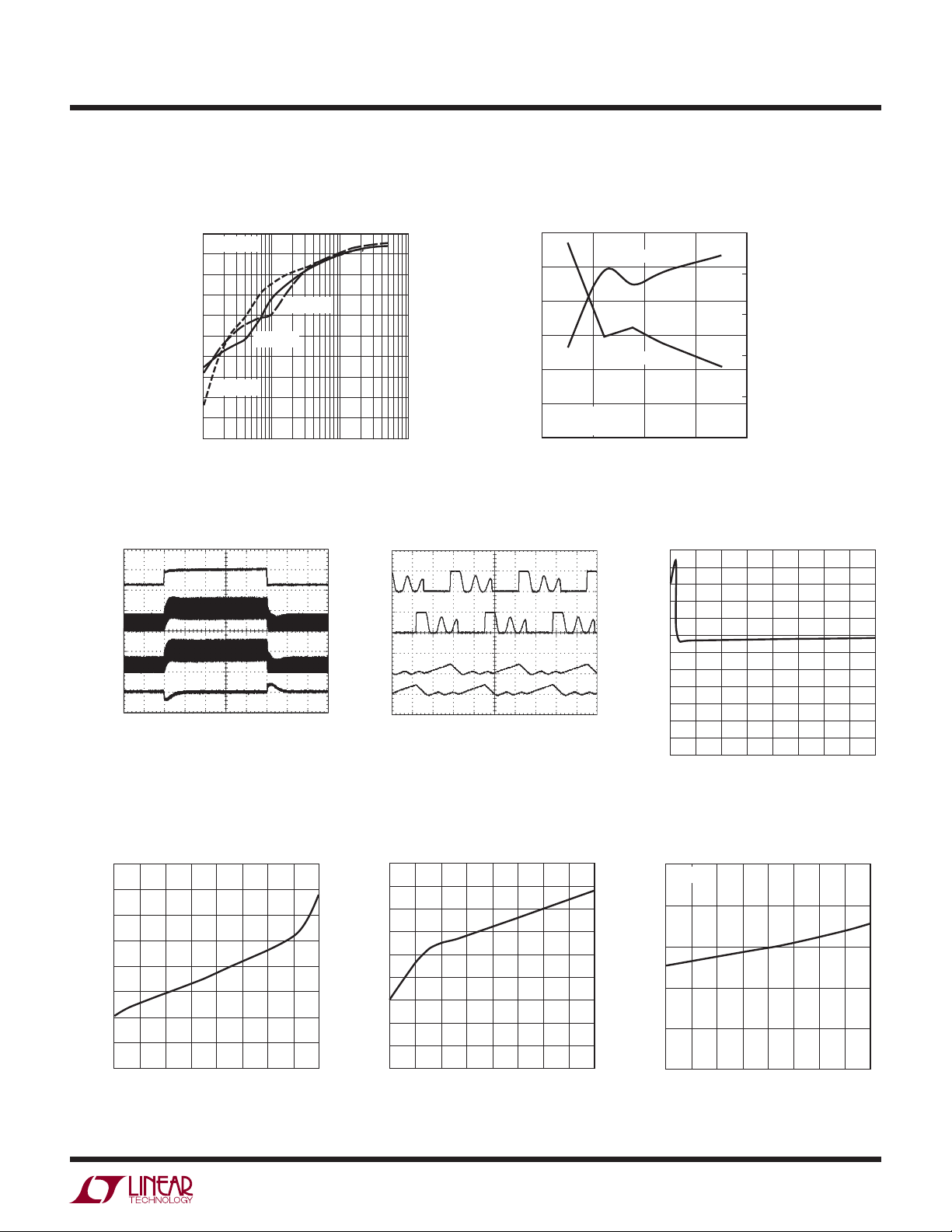
TYPICAL PERFORMANCE CHARACTERISTICS
Effi ciency and Power Loss vs
Input Voltage
96
95
94
93
EFFICIENCY (%)
92
91
90
0
I
LOAD
5A/DIV
1A TO 5A
5A/DIV
5A/DIV
V
OUT
500mV/DIV
Effi ciency vs Output Current
100
V
= 48V
OUT
95
90
85
80
75
70
EFFICIENCY (%)
65
VIN = 12V
60
55
50
10
VIN = 35V
VIN = 24V
100 1000 10000
LOAD CURRENT (mA)
3862 G01
Load Step Inductor Current at Light Load
SW1
50V/DIV
I
L1
I
L2
3862 G03
V
IN
OUT
= 24V
= 48V
500µs/DIVV
SW2
50V/DIV
2A/DIV
2A/DIV
I
L1
I
L2
V
I
LOAD
= 12V
IN
OUT
= 48V
= 100mA
1µs/DIVV
EFFICIENCY
POWER LOSS
V
= 48V
OUT
= 1A
I
OUT
10 20 30 40
INPUT VOLTAGE (V)
3.00
2.75
2.50
2.25
2.00
1.75
1.50
1.25
1.00
0.75
3862 G04
QUIESCENT CURRENT (mA)
0.50
0.25
LTC3862
4000
3500
POWER LOSS (mW)
3000
2500
2000
1500
3862 G02
Quiescent Current vs Input
Voltage
0
4
12 16 20
8
INPUT VOLTAGE (V)
24 28 32 36
3862 G05
Quiescent Current vs Temperature
1.90
1.85
1.80
1.75
1.70
1.65
1.60
QUIESCENT CURRENT (mA)
1.55
1.50
–50
–25
0
50
25
TEMPERATURE (°C)
75
100
125
3862 G06
150
Shutdown Quiescent Current vs
Input Voltage
45
40
35
30
25
20
15
SHUTDOWN CURRENT (µA)
10
5
0
8
4
12
20
16
INPUT VOLTAGE (V)
24
Shutdown Quiescent Current vs
Temperature
50
VIN = 12V
40
30
20
SHUTDOWN CURRENT (µA)
10
32
3862 G07
36
28
0
–50
–25 0
50
25 75 150
TEMPERATURE (°C)
100 125
3862 G08
3862fa
5
LTC3862
TYPICAL PERFORMANCE CHARACTERISTICS
INTVCC Line Regulation INTVCC Load Regulation INTVCC vs Temperature
5.25
5.00
VOLTAGE (V)
CC
INTV
4.75
51015 25
0
INPUT VOLTAGE (V)
5.00
4.95
4.90
VOLTAGE (V)
CC
INTV
4.85
20
3962 G09
4.80
10
0
INTVCC LOAD CURRENT (mA)
30
40
20
50
3862 G10
5.00
4.99
4.98
4.97
4.96
4.95
VOLTAGE (V)
4.94
CC
4.93
INTV
4.92
4.91
4.90
–50
–25 25
0
50
TEMPERATURE (°C)
125
100
75
150
3862 G11
INTVCC LDO Dropout vs Load
Current, Temperature
1600
1400
1200
1000
800
600
400
DROPOUT VOLTAGE (mV)
200
0
10 20 40
0
INTVCC LOAD (mA)
Feedback Voltage Line
Regulation
1.226
1.225
1.224
1.223
FB VOLTAGE (V)
1.222
1.221
1.220
4
12 20
816
INPUT VOLTAGE (V)
125°C
30
24
150°C
28
85°C
25°C
–40°C
3862 G12
32
3862 G15
INTVCC UVLO Threshold vs
Temperature
3.6
3.5
3.4
3.3
3.2
3.1
VOLTAGE (V)
3.0
CC
2.9
INTV
2.8
2.7
50
2.6
–50
–25 25
Current Sense Threshold vs
ITH Voltage
80
70
60
50
40
30
20
CURRENT SENSE THRESHOLD (mV)
10
36
0
0 0.4 0.8 1.2 1.6 2.0 2.4
0
50
TEMPERATURE (°C)
ITH VOLTAGE (V)
Feedback Voltage vs Temperature
1.235
1.233
1.231
1.229
1.227
1.225
1.223
1.221
FB VOLTAGE (V)
1.219
1.217
1.215
1.213
1.211
125
100
75
150
3862 G13
–50
02550
–25
TEMPERATURE (°C)
75 100 125 150
3862 G14
Current Sense Threshold vs
Temperature
80
79
78
77
76
75
74
73
72
CURRENT SENSE THRESHOLD (mV)
71
3862 G16
70
–50
–25 25
0
TEMPERATURE (°C)
50
75
100
125
150
3862 G17
6
3862fa

TYPICAL PERFORMANCE CHARACTERISTICS
Maximum Current Sense
Threshold vs Duty Cycle
80
RUN Threshold vs Temperature RUN Threshold vs Input Voltage
1.30
LTC3862
1.5
75
70
65
60
55
MAXIMUM CURRENT SENSE THRESHOLD (mV)
50
20 40 60 80
DUTY CYCLE (%)
SLOPE = 0.625
SLOPE = 1
SLOPE = 1.66
RUN (Off) Source Current vs
Temperature
0
–0.1
–0.2
–0.3
–0.4
–0.5
–0.6
–0.7
RUN PIN CURRENT (µA)
–0.8
–0.9
–1.0
–50
–25 25
0
50
TEMPERATURE (°C)
100
75
3862 G18
125
3862 G21vv
100100 30507090
150
1.25
1.20
RUN PIN VOLTAGE (V)
1.15
1.10
–50
–25 0 25 50
TEMPERATURE (°C)
RUN (On) Source Current vs
Temperature
0
–1
–2
–3
–4
–5
RUN PIN CURRENT (µA)
–6
–7
–8
–25
–50
0
50
25
TEMPERATURE (°C)
ON
OFF
75
75
100 125 150
3862 G09
125
150
1344 G06
100
1.4
1.3
1.2
RUN PIN VOLTAGE (V)
1.1
1.0
0
510
15 25 40
INPUT VOLTAGE (V)
RUN Source Current vs
Input Voltage
0
–1
–2
–3
–4
–5
RUN PIN CURRENT (µA)
–6
–7
48
12 16 203224 36
INPUT VOLTAGE (V)
ON
OFF
20
30 35
3862 G20
28
3862 G23
Soft-Start Current vs Temperature
–5.0
–5.1
–5.2
–5.3
–5.4
SOFT-START CURRENT (µA)
–5.5
–5.6
–50
050
–25 25
TEMPERATURE (°C)
75
100
125
3862 G24
150
Soft-Start Current vs
Soft-Start Voltage
0
–1
–2
–3
–4
SOFT-START CURRENT (µA)
–5
–6
0
12
0.5 1.5
SOFT-START VOLTAGE (V)
2.5
Oscillator Frequency vs
Temperature
307
306
305
304
303
302
301
FREQUENCY (kHz)
300
299
3
3.5
4
3862 G25
298
–50
–25
0
50
25
TEMPERATURE (°C)
75
100
125
150
3862 G26
3862fa
7
LTC3862
TYPICAL PERFORMANCE CHARACTERISTICS
Oscillator Frequency vs
R
Input Voltage
320
315
310
305
300
295
FREQUENCY (kHz)
290
285
280
436
0
16
8
12
INPUT VOLTAGE (V)
1000
(k)
100
FREQ
R
20
32
24
28
3862 G27
10
vs Frequency
FREQ
200 1000
100
0
400
500
300
FREQUENCY (kHz)
Frequency vs PLLFLTR Voltage
1400
1200
1000
800
600
FREQUENCY (kHz)
400
200
800700600
900
3862 G28
0
0.5 1 1.5 2.5
0
PLLFLTR VOLTAGE (V)
2
3862 G29
Frequency Voltage vs
Temperature
1.235
1.233
1.231
1.229
1.227
1.225
1.223
1.221
1.219
FREQ VOLTAGE (V)
1.217
1.215
1.213
1.211
–50
–25
0
50
25
TEMPERATURE (°C)
75
100
125
150
3862 G30
Gate Turn-On Waveform Driving
Renesas HAT2266
GATE
1V/DIV
Minimum On-Time vs
Temperature
400
350
300
250
200
MINIMUM ON-TIME (ns)
150
100
–50
050
–25 25
TEMPERATURE (°C)
BLANK = 3V8
BLANK = FLOAT
BLANK = SGND
75
Minimum On-Time vs
Input Voltage
400
350
300
250
200
MINIMUM ON-TIME (ns)
150
100
125
150
3862 G31
100
4
Gate Turn-Off Waveform Driving
Renesas HAT2266
GATE
1V/DIV
BLANK = 3V8
BLANK = FLOAT
BLANK = SGND
12 20
816
INPUT VOLTAGE (V)
28
24
32
36
3862 G32
8
= 12V
IN
OUT = 48V
V
OUT = 1A
I
MOSFET RENESAS HAT2266
20ns/DIVV
3862 G33
= 12V
IN
OUT = 48V
V
OUT = 1A
I
MOSFET RENESAS HAT2266
20ns/DIVV
3862 G34
3862fa

PIN FUNCTIONS
LTC3862
3V8: Output of the Internal 3.8V LDO from INTVCC. Supply
pin for the low voltage analog and digital circuits. A low
ESR 1nF ceramic bypass capacitor should be connected
between 3V8 and SGND, as close as possible to the IC.
BLANK: Blanking Time. Floating this pin provides a nominal
minimum on-time of 260ns. Connecting this pin to 3V8
provides a minimum on-time of 340ns, while connecting
it to SGND provides a minimum on-time of 180ns.
CLKOUT: Digital Output Used for Daisy-Chaining Multiple
LTC3862 ICs in Multi-Phase Systems. The PHASEMODE
pin voltage controls the relationship between CH1 and
CH2 as well as between CH1 and CLKOUT.
: Maximum Duty Cycle.This pin programs the maxi-
D
MAX
mum duty cycle. Floating this pin provides 84% duty cycle.
Connecting this pin to 3V8 provides 75% duty cycle, while
connecting it to SGND provides 96% duty cycle.
FB: Error Amplifi er Input. The FB pin should be connected
through a resistive divider network to V
output voltage.
FREQ: A resistor from FREQ to SGND sets the operating
frequency.
GATE1, GATE2: Gate Drive Output. The LTC3862 provides
a 5V gate drive referenced to PGND to drive a logic-level
threshold MOSFET.
INTV
(LDO). A low ESR 4.7µF (X5R or better) ceramic bypass
capacitor should be connected between INTV
as close as possible to the IC.
: Output of the Internal 5V Low Dropout Regulator
CC
to set the
OUT
and PGND,
CC
ITH: Error Amplifi er Output. The current comparator trip
threshold increases with the ITH control voltage. The ITH
pin is also used for compensating the control loop of the
converter.
PGND: Power Ground. Connect this pin close to the
sources of the power MOSFETs. PGND should also be
connected to the negative terminals of V
bypass capacitors. PGND is electrically isolated from the
SGND pin. The Exposed Pad of the FE and QFN packages
is connected to PGND.
PHASEMODE: The PHASEMODE pin voltage programs
the phase relationship between CH1 and CH2 rising gate
signals, as well as the phase relationship between CH1
gate signal and CLKOUT. Floating this pin or connecting
it to either 3V8, or SGND changes the phase relationship
between CH1, CH2 and CLKOUT.
PLLFLTR: PLL Lowpass Filter Input. When synchronizing to an external clock, this pin serves as the lowpass
fi lter input for the PLL. A series resistor and capacitor
connected from PLLFLTR to SGND compensate the PLL
feedback loop.
RUN: Run Control Input. A voltage above 1.22V on the pin
turns on the IC. Forcing the pin below 1.22V causes the
IC to shut down. There is a 0.5µA pull-up current for this
pin. Once the RUN pin raises above 1.22V, an additional
4.5µA pull-up current is added to the pin for programmable hysteresis.
and INTVCC
IN
3862fa
9

LTC3862
PIN FUNCTIONS
SENSE1+, SENSE2+: Positive Inputs to the Current
Comparators. The ITH pin voltage programs the current
comparator offset in order to set the peak current trip
threshold. This pin is normally connected to a sense
resistor in the source of the power MOSFET.
–
SENSE1
parators. This pin is normally connected to the bottom of
the sense resistor.
SGND: Signal Ground. All feedback and soft-start connections should return to SGND. For optimum load
regulation, the SGND pin should be kelvin connected to
the PCB location between the negative terminals of the
output capacitors.
SLOPE: This pin programs the gain of the internal slope
compensation. Floating this pin provides a normalized
slope compensation gain of 1.00. Connecting this pin
to 3V8 increases the normalized slope compensation by
, SENSE2–: Negative Inputs to the Current Com-
66%, and connecting it to SGND decreases the normalized
slope compensation by 37.5%. See Applications Information for more details.
SS: Soft-Start Input. For soft-start operation, connecting
a capacitor from this pin to SGND will clamp the output of
the error amp. An internal 5µA current source will charge
the capacitor and set the rate of increase of the peak switch
current of the converter.
SYNC: PLL Synchronization Input. Applying an external
clock between 50kHz and 650kHz will cause the operating
frequency to synchronize to the clock. SYNC is pulled down
by a 50k internal resistor. The rising edge of the SYNC
input waveform will align with the rising edge of GATE1
in closed-loop operation.
: Main Supply Input. A low ESR ceramic capacitor
V
IN
should be connected between this pin and SGND.
10
3862fa
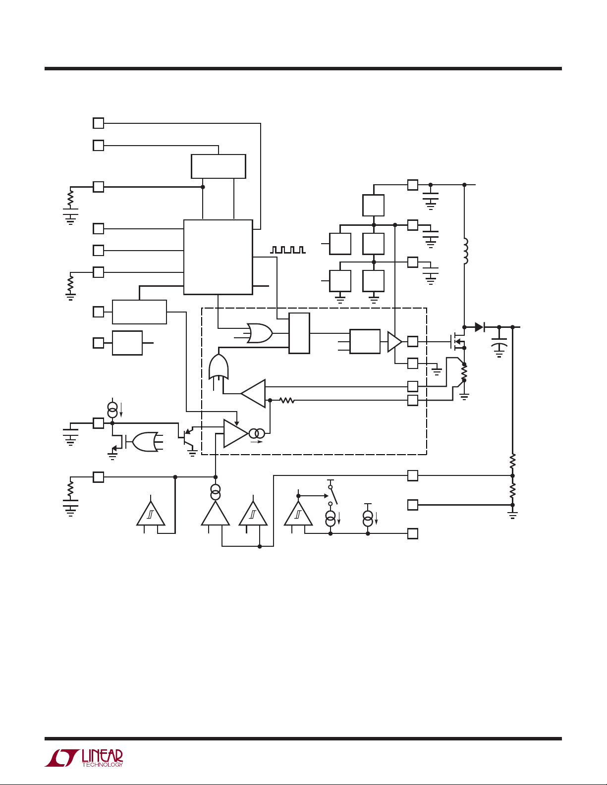
FUNCTIONAL DIAGRAM
CLKOUT
SYNC
PLLFLTR
R
P
C
P
D
MAX
PHASEMODE
FREQ
R
FREQ
SLOPE
BLANK
SS
SLOPE
COMPENSATION
BLANK
LOGIC
3V8
5µA
BLOGIC
DETECT
PSKIP
SYNC
VCO
OV
UV
ITRIP
LTC3862
V
IN
C
5V
LDO
UVLO
LOOP
S
R1 Q
R2
UV
OT
OVER
TEMP
SD
BLOGIC
CLK1
CLK2
D
MAX
OT
PWM LATCH
+
R
ICMP
–
3.8V
LDO
BIAS
LOGIC
INTV
3V8
GATE
PGND
SENSE
SENSE
IN
CC
C
VCC
C
3V8
+
–
V
IN
L
D
+
M
C
OUT
R
S
V
OUT
C
SS
ITH
R
C
C
C
PSKIP
0.275V
PSKIP
–
OT
UV
SD
+
+
1.223V
V TO I
RUN
–
1.22V
SD
+
OV
OV
EA
–
–
+
1.345V
4.5µA
DUPLICATE FOR
SECOND CHANNEL
V
FB
SGND
0.5µA
RUN
R2
R1
3862 FD
3862fa
11
LTC3862
OPERATION
The Control Loop
The LTC3862 uses a constant frequency, peak current
mode step-up architecture with its two channels operating 180 degrees out of phase. During normal operation,
each external MOSFET is turned on when the clock for
that channel sets the PWM latch, and is turned off when
the main current comparator, ICMP, resets the latch. The
peak inductor current at which ICMP trips and resets the
latch is controlled by the voltage on the ITH pin, which is
the output of the error amplifi er, EA. The error amplifi er
compares the output feedback signal at the V
pin to the
FB
internal 1.223V reference and generates an error signal
at the ITH pin. When the load current increases it causes
a slight decrease in V
relative to the reference voltage,
FB
which causes the EA to increase the ITH voltage until the
average inductor current matches the new load current.
After the MOSFET is turned off, the inductor current fl ows
through the boost diode into the output capacitor and load,
until the beginning of the next clock cycle.
Cascaded LDOs Supply Power to the Gate Driver and
Control Circuitry
The LTC3862 contains two cascaded PMOS output stage
low dropout voltage regulators (LDOs), one for the gate
drive supply (INTV
) and one for the low voltage analog
CC
and digital control circuitry (3V8). A block diagram of this
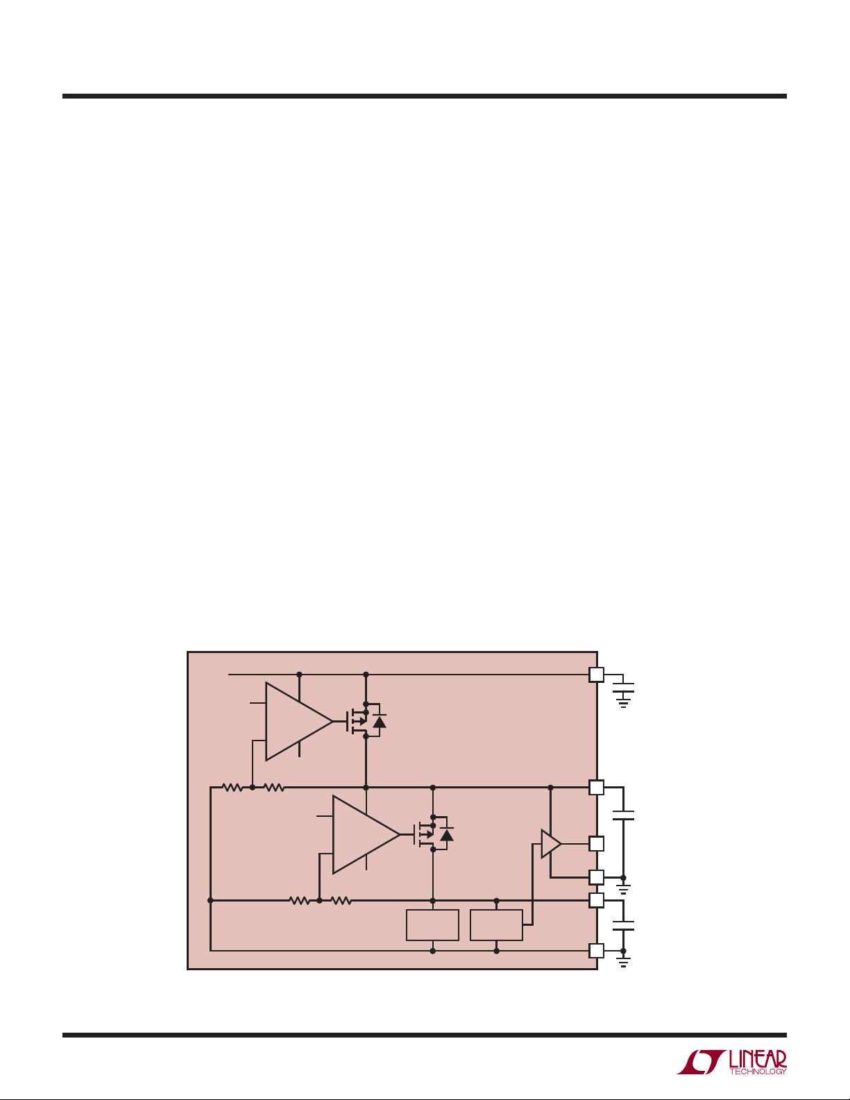
power supply arrangement is shown in Figure 1.
The Gate Driver Supply LDO (INTV
The 5V output (INTV
and supplies power to the power MOSFET gate driv-
V
IN
ers. The INTV
pin should be bypassed to PGND with a
CC
) of the fi rst LDO is powered from
CC
CC
)
minimum of 4.7F of ceramic capacitance (X5R or better),
placed as close as possible to the IC pins. If two power
MOSFETs are connected in parallel for each channel in
order to increase the output power level, or if a single
MOSFET with a Q
greater than 50nC is used, then it is
G
recommended that the bypass capacitance be increased
to a minimum of 10F.
An undervoltage lockout (UVLO) circuit senses the INTV
CC
regulator output in order to protect the power MOSFETs
from operating with inadequate gate drive. For the LTC3862
the rising UVLO threshold is typically 3.3V and the hysteresis is typically 400mV. The LTC3862 was optimized for
logic-level power MOSFETs and applications where the
output voltage is less than 50V to 60V. For applications
requiring standard threshold power MOSFETs, please refer
to the LTC3862-1 data sheet.
LTC3862
1.223V
–
+
R2 R1
Figure 1. Cascaded LDOs Provide Gate Drive and Control Circuitry Power
SGND
1.223V
R4
NOTE: PLACE C
VCC
–
+
R3
AND C
P-CH
INTV
CC
P-CH
SGND
CAPACITORS AS CLOSE AS POSSIBLE TO DEVICE PINS
3V8
3V8
ANALOG
CIRCUITS
LOGIC
INTV
V
GATE
PGND
3V8
SGND
IN
C
IN
CC
C
VCC
C
3V8
3862 F01
3862fa
12

OPERATION
LTC3862
In multi-phase applications, all of the FB pins are connected
together and all of the error amplifi er output pins (ITH) are
connected together. The INTV
be connected together. The INTV
pins, however, should not
CC
regulator is capable of
CC
sourcing current but is not capable of sinking current. As
a result, when two or more INTV
regulator outputs are
CC
connected together, the highest voltage regulator supplies
all of the gate drive and control circuit current, and the
other regulators are off. This would place a thermal burden
on the highest output voltage LDO and could cause the
maximum die temperature to be exceeded. In multi-phase
LTC3862 applications, each INTV
regulator output should
CC
be independently bypassed to its respective PGND pin as
close as possible to each IC.
The Low Voltage Analog and Digital Supply LDO (3V8)
The second LDO within the LTC3862 is powered off of
INTV
and serves as the supply to the low voltage analog
CC
and digital control circuitry, as shown in Figure 1. The
output voltage of this LDO (which also has a PMOS output device) is 3.8V. Most of the analog and digital control
circuitry is powered from the internal 3V8 LDO. The 3V8
pin should be bypassed to SGND with a 1nF ceramic capacitor (X5R or better), placed as close as possible to the
IC pins. This LDO is not intended to be used as a supply
for external circuitry.
the maximum junction temperature of the IC is never
exceeded. The junction temperature can be estimated
using the following equations:
I
P
T
= IQ + Q
Q(TOT)
= VIN • (IQ + Q
DISS
= TA + P
J
DISS
The total quiescent current (I
supply current (I
• f
G(TOT)
• f)
G(TOT)
• R
TH(JA)
) consists of the static
Q(TOT)
) and the current required to charge
Q
the gate capacitance of the power MOSFETs. The value
of Q
should come from the plot of VGS vs QG in the
G(TOT)
Typical Performance Characteristics section of the MOSFET
data sheet. The value listed in the electrical specifi cations
may be measured at a higher V
value of interest is at the 5V INTV
, such as 10V, whereas the
GS
gate drive voltage.
CC
As an example of the required thermal analysis, consider
a 2-phase boost converter with a 9V to 24V input voltage
range and an output voltage of 48V at 2A. The switching
frequency is 150kHz and the maximum ambient temperature is 70°C. The power MOSFET used for this application
is the Vishay Si7478DP, which has a typical R
8.8m at V
plot of V
= 4.5V and 7.5m at VGS = 10V. From the
GS
vs QG, the total gate charge at VGS = 5V is
GS
DS(ON)
of
50nC (the temperature coeffi cient of the gate charge is
low). One power MOSFET is used for each phase. For the
QFN package option:
Thermal Considerations and Package Options
The LTC3862 is offered in two package options. The 5mm
× 5mm QFN package (UH24) has a thermal resistance
R
of 34°C/W, the 24-pin TSSOP (FE24) package has a
TH(JA)
thermal resistance of 38°C/W, and the 24-pin SSOP (GN24)
package has a thermal resistance of 85°C/W. The QFN and
TSSOP package options have a lead pitch of 0.65mm, and
the GN24 option has a lead pitch of 0.025in.
The INTV
regulator can supply up to 50mA of total
CC
current. As a result, care must be taken to ensure that
I
P
T
= 3mA + 2 • 50nC • 150kHz = 18mA
Q(TOT)
= 24V • 18mA = 432mW
DISS
= 70°C + 432mW • 34°C/W = 84.7°C
J
In this example, the junction temperature rise is only 14.7°C.
These equations demonstrate how the gate charge current
typically dominates the quiescent current of the IC, and
how the choice of package option and board heat sinking
can have a signifi cant effect on the thermal performance
of the solution.
3862fa
13

LTC3862
OPERATION
To prevent the maximum junction temperature from being exceeded, the input supply current to the IC should
be checked when operating in continuous mode (heavy
load) at maximum V
. A tradeoff between the operating
IN
frequency and the size of the power MOSFETs may need
to be made in order to maintain a reliable junction temperature. Finally, it is important to verify the calculations
by performing a thermal analysis of the fi nal PCB using
an infrared camera or thermal probe. As an option, an
exernal regulator shown in Figure 3 can be used to reduce
the total power dissipation on the IC.
Thermal Shutdown Protection
In the event of an overtemperature condition (external
or internal), an internal thermal monitor will shut down
the gate drivers and reset the soft-start capacitor if the
die temperature exceeds 170°C. This thermal sensor
has a hysteresis of 10°C to prevent erratic behavior at
hot temperatures. The LTC3862’s internal thermal sensor is intended to protect the device during momentary
overtemperature conditions. Continuous operation above
the specifi ed maximum operating junction temperature,
however, may result in device degradation.
Operation at Low Supply Voltage
If the input voltage V
is low enough for the INTVCC LDO
IN
to be in dropout, then the minimum gate drive supply
voltage is:
V
INTVCC
= V
IN(MIN)
– V
DROPOUT
The LDO dropout voltage is a function of the total gate
drive current and the quiescent current of the IC (typically
3mA). A curve of dropout voltage vs output current for the
LDO is shown in Figure 2. The temperature coeffi cient of
the LDO dropout voltage is approximately 6000ppm/°C.
The total Q-current (I
) fl owing in the LDO is the sum
Q(TOT)
of the controller quiescent current (3mA) and the total gate
charge drive current.
I
Q(TOT)
= IQ + Q
G(TOT)
• f
After the calculations have been completed, it is important to measure the gate drive waveforms and the gate
driver supply voltage (INTV
conditions (low V
, nominal VIN and high VIN, as well
IN
to PGND) over all operating
CC
as from light load to full load) to ensure adequate power
MOSFET enhancement. Consult the power MOSFET data
sheet to determine the actual R
, and verify your thermal calculations by measuring
V
GS
for the measured
DS(ON)
the component temperatures using an infrared camera
or thermal probe.
The LTC3862 has a minimum input voltage of 4V, making
it a good choice for applications that experience low supply conditions. The gate driver for the LTC3862 consists
of PMOS pull-up and NMOS pull-down devices, allowing
the full INTV
voltage to be applied to the gates during
CC
power MOSFET switching. Nonetheless, care should be
taken to determine the minimum gate drive supply voltage
(INTV
) in order to choose the optimum power MOSFETs.
CC
Important parameters that can affect the minimum gate
drive voltage are the minimum input voltage (V
the LDO dropout voltage, the Q
of the power MOSFETs,
G
IN(MIN)
),
and the operating frequency.
1600
1400
1200
1000
800
600
DROPOUT VOLTAGE (mV)
400
200
0
Figure 2. INTVCC LDO Dropout Voltage vs Current
10 20 40
0
INTVCC LOAD (mA)
125°C
30
150°C
85°C
25°C
–40°C
50
3862 F02
3862fa
14

OPERATION
LTC3862
Operation at High Supply Voltage
At high input voltages, the LTC3862’s internal LDO can
dissipate a signifi cant amount of power, which could
cause the maximum junction temperature to be exceeded.
Conditions such as a high operating frequency, or the use
of more than one power MOSFET per channel, could push
the junction temperature rise to high levels. If the thermal
equations above indicate too high a rise in the junction
temperature, an external bias supply can always be used
to reduce the power dissipation on the IC, as shown in
Figure 3.
For example, a 5V or 12V system rail that is available
would be more suitable than the 24V main input power
rail to power the LTC3862. Also, the bias power can be
generated with a separate switching or LDO regulator. An
example of an LDO regulator is shown in Figure 3. The
output voltage of the LDO regulator can be set by selecting
an appropriate zener diode to be higher than 5V but low
enough to divide the power dissipation between LTC3862
and Q1 in Figure 3. The absolute maximum voltage rating
of the INTV
pin is 6V.
CC
fl ow from the external INTV
supply, through the body
CC
diode of the LDO PMOS device, to the input capacitor
and V
pin. This high current fl ow could trigger a latchup
IN
condition and cause catastrophic failure of the IC.
If, however, the V
INTV
supply, the external INTVCC supply will act as a
CC
supply to the IC comes up before the
IN
load to the internal LDO in the LTC3862, and the LDO will
attempt to charge the INTV
output with its short-circuit
CC
current. This will result in excessive power dissipation and
possible thermal overload of the LTC3862.
If an independent 5V supply exists in the system, it may be
possible to short INTV
reduce gate drive power dissipation. With V
and VIN together to 5V in order to
CC
and INTVCC
IN
shorted together, the LDO output PMOS transistor is biased
= 0V, and the current demand of the internal analog
at V
DS
and digital control circuitry, as well as the gate drive current, will be supplied by the external 5V supply.
Programming the Output Voltage
The output voltage is set by a resistor divider according
to the following formula:
V
IN
R1
Q1
D1
(OPT)
C
VCC
Figure 3. Using the LTC3862 with an External Bias Supply
V
IN
LTC3862
INTV
CC
3862 F03
Power Supply Sequencing
As shown in Figure 1, there are body diodes in parallel
with the PMOS output transistors in the two LDO regulators in the LTC3862. As a result, it is not possible to bias
the INTV
supplies. Independently biasing the INTV
and VIN pins of the chip from separate power
CC
pin from a
CC
separate power supply can cause one of two possible
failure modes during supply sequencing. If the INTV
supply comes up before the V
supply, high current will
IN
CC
1 223 1
⎛
VV
OUT
.
=+
⎜
⎝
⎞
2
R
⎟
1
R
⎠
The external resistor divider is connected to the output
as shown in Figure 4. Resistor R1 is normally chosen so
that the output voltage error caused by the current fl owing
out of the V
pin during normal operation is negligible
FB
compared to the current in the divider. For an output voltage error due to the error amp input bias current of less
than 0.5%, this translates to a maximum value of R1 of
about 30k.
V
OUT
LTC3862
FB
SGND
Figure 4. Programming the Output Voltage
with a Resistor Divider
R2
R1
3862 F04
3862fa
15

LTC3862
OPERATION
Operation of the RUN Pin
The control circuitry in the LTC3862 is turned on and
off using the RUN pin. Pulling the RUN pin below 1.22V
forces shutdown mode and releasing it allows a 0.5A
current source to pull this pin up, allowing a “normally
on” converter to be designed. Alternatively, the RUN pin
can be externally pulled up or driven directly by logic.
Care must be taken not to exceed the absolute maximum
rating of 8V for this pin.
The comparator on the RUN pin can also be used to sense
the input voltage, allowing an undervoltage detection
circuit to be designed. This is helpful in boost converter
applications where the input current can reach very high
levels at low input voltage:
IV
•
OUT OUT
I
=
IN
V
• η
IN
The 1.22V input threshold of the RUN comparator is derived
from a precise bandgap reference, in order to maximize
the accuracy of the undervoltage-sensing function. The
RUN comparator has 80mV built-in hysteresis. When
the voltage on the RUN pin exceeds 1.22V, the current
sourced into the RUN pin is switched from 0.5A to 5A
PTAT current. The user can therefore program both the
rising threshold and the amount of hysteresis using the
values of the resistors in the external divider, as shown in
the following equations:
V
IN
INTERNAL 5V
0.5µA
RUN
10V
SGND
1.22V
4.5µA
+
–
RUN
COMPARATOR
LTC3862
BIAS AND
START-UP
CONTROL
3862 F05a
Figure 5a. Using the RUN Pin for a “Normally On” Converter
EXTERNAL
LOGIC
CONTROL
V
0.5µA
RUN
10V
SGND
IN
INTERNAL 5V
1.22V
4.5µA
+
–
RUN
COMPARATOR
LTC3862
BIAS AND
START-UP
CONTROL
3862 F05b
Figure 5b. On/Off Control Using External Logic
VV
IN ON
()
.–.•=+
122 1 05
⎜
⎝
⎛
⎛
.. – •22 1 5V
=
1
⎜
⎝
V
IN OFF
()
⎞
R
A
⎟
R
⎠
B
R
A
+
R
B
µR
A
⎞
µR
⎟
⎠
A
Several of the possible RUN pin control techniques are
illustrated in Figure 5.
Frequency Selection and the Phase Lock Loop
The selection of the switching frequency is a tradeoff
between effi ciency and component size. Low frequency
operation increases effi ciency by reducing MOSFET
switching losses, but requires a larger inductor and output
capacitor to maintain low output ripple.
16
R
R
A
B
V
0.5µA
RUN
10V
SGND
IN
INTERNAL 5V
1.22V
4.5µA
+
–
RUN
COMPARATOR
LTC3862
BIAS AND
START-UP
CONTROL
3862 F05c
Figure 5c. Programming the Input Voltage Turn-On and Turn-Off
Thresholds Using the RUN Pin
3862fa

OPERATION
LTC3862
The LTC3862 uses a constant frequency architecture that
can be programmed over a 75kHz to 500kHz range using
a single resistor from the FREQ pin to ground. Figure 6
illustrates the relationship between the FREQ pin resistance
and the operating frequency.
The operating frequency of the LTC3862 can be approximated using the following formula:
R
FREQ
= 5.5096E9(f
OSC
–0.9255
)
A phase-lock loop is available on the LTC3862 to synchronize the internal oscillator to an external clock source
connected to the SYNC pin. Connect a series RC network
from the PLLFLTR pin to SGND to compensate PLL’s
feedback loop. Typical compensation components are a
0.01F capacitor in series with a 10k resistor. The PLLFLTR
pin is both the output of the phase detector and the input
to the voltage controlled oscillator (VCO). The LTC3862
phase detector adjusts the voltage on the PLLFLTR pin
to align the rising edge of GATE1 to the leading edge of
the external clock signal, as shown in Figure 7. The rising edge of GATE2 will depend upon the voltage on the
PHASEMODE pin. The capture range of the LTC3862’s PLL
is 50kHz to 650kHz.
Because the operating frequency of the LTC3862 can be
programmed using an external resistor, in synchronized
applications, it is recommended that the free-running frequency (as defi ned by the external resistor) be set to the
same value as the synchronized frequency. This results in
a start-up of the IC at approximately the same frequency
as the external clock, so that when the sync signal comes
alive, no discontinuity at the output will be observed. It also
ensures that the operating frequency remains essentially
constant in the event the sync signal is lost. The SYNC
pin has an internal 50k resistor to ground.
Using the CLKOUT and PHASEMODE Pins
in Multi-Phase Applications
The LTC3862 features two pins (CLKOUT and PHASEMODE)
that allow multiple ICs to be daisy-chained together for
higher current multi-phase applications. For a 3- or 4-phase
1000
(k)
100
FREQ
R
10
Figure 6. FREQ Pin Resistor Value vs Frequency
SYNC
10V/DIV
GATE1
10V/DIV
GATE2
10V/DIV
CLKOUT
10V/DIV
V
PHASEMODE = SGND
Figure 7: Synchronization of the LTC3862
to an External Clock Using the PLL
200 1000
400
500
300
FREQUENCY (kHz)
2µs/DIVV
IN
OUT
0
= 12V
100
= 48V 1A
800700600
900
3862 F06
3862 F07
design, the CLKOUT signal of the master controller is connected to the SYNC input of the slave controller in order
to synchronize additional power stages for a single high
current output. The PHASEMODE pin is used to adjust the
phase relationship between channel 1 and channel 2, as well
as the phase relationship between channel 1 and CLKOUT,
as summarized in Table 1. The phases are calculated relative to the zero degrees, defi ned as the rising edge of the
GATE1 output. In a 6-phase application the CLKOUT pin
of the master controller connects to the SYNC input of the
2nd controller and the CLKOUT pin of the 2nd controller
connects to the SYNC pin of the 3rd controller.
3862fa
17

LTC3862
OPERATION
Table 1
PHASEMODE
SGND 180° 90° 2-Phase, 4-Phase
Float 180° 60° 6-Phase
3V8 120° 240° 3-Phase
CH-1 to CH-2
PHASE
CH-1 to CLKOUT
PHASE APPLICATION
Using the LTC3862 Transconductance (gm) Error
Amplifi er in Multi-Phase Applications
The LTC3862 error amplifi er is a transconductance, or g
m
amplifi er, meaning that it has high DC gain but high output
impedance (the output of the error amplifi er is a current
proportional to the differential input voltage). This style
of error amplifi er greatly eases the task of implementing
a multi-phase solution, because the amplifi ers from two
or more chips can be connected in parallel. In this case
the FB pins of multiple LTC3862s can be connected together, as well as the ITH pins, as shown in Figure 8. The
of the composite error amplifi er is simply n times the
g
m
transconductance of one amplifi er, or g
m(TOT)
= n • 660S,
where n is the number of amplifi ers connected in parallel. The transfer function from the ITH pin to the current
comparator inputs was carefully designed to be accurate,
both from channel-to-channel and chip-to-chip. This way
the peak inductor current matching is kept accurate.
A buffered version of the output of the error amplifi er
determines the threshold at the input of the current comparator. The ITH voltage that represents zero peak current
is 0.4V and the voltage that represents current limit is
1.2V (at low duty cycle). During an overload condition, the
output of the error amplifi er is clamped to 2.6V at low duty
cycle, in order to reduce the latency when the overload
condition terminates. A patented circuit in the LTC3862 is
used to recover the slope compensation signal, so that the
maximum peak inductor current is not a strong function
of the duty cycle.
Soft-Start
MASTER
V
OUT
ALL ITH PINS
CONNECTED
TOGETHER
ALL FB PINS
CONNECTED
TOGETHER
FREQ
ITH
FB
CLKOUT
SYNC
PLLFLTR
FREQ
ITH
FB
CLKOUT
SYNC
PLLFLTR
FREQ
ITH
FB
CLKOUT
SYNC
PLLFLTR
LTC3862
SGND
SLAVE
LTC3862
SGND
SLAVE
LTC3862
SGND
INTV
INTV
INTV
RUN
RUN
RUN
CC
SS
CC
SS
CC
SS
3862 F08
ON/OFF
CONTROL
INDIVIDUAL
PINS
INTV
CC
LOCALLY
DECOUPLED
ALL RUN PINS
CONNNECTED
TOGETHER
ALL SS PINS
CONNNECTED
TOGETHER
Figure 8. LTC3862 Error Amplifi er Confi guration
for Multi-Phase Operation
buffered ITH node (please note that the ITH pin voltage may
not track the soft-start voltage during this time period).
An internal 5A current source charges the SS capacitor,
and clamps the peak sense threshold until the voltage on
the soft-start capacitor reaches approximately 0.6V. The
required amount of soft-start capacitance can be estimated
using the following equation:
CµA
=
5
SS
⎛
⎜
⎝
06.
⎞
t
SS
⎟
V
⎠
The start-up of the LTC3862 is controlled by the voltage on
the SS pin. An internal PNP transistor clamps the current
comparator sense threshold during soft-start, thereby
limiting the peak switch current. The base of the PNP is
connected to the SS pin and the emitter to an internal,
18
The SS pin has an internal open-drain NMOS pull-down
transistor that turns on when the RUN pin is pulled low,
when the voltage on the INTV
pin is below its undervoltage
CC
lockout threshold, or during an overtemperature condition. In multi-phase applications that use more than one
3862fa

OPERATION
LTC3862
LTC3862 chip, connect all of the SS pins together and use
one external capacitor to program the soft-start time. In
this case, the current into the soft-start capacitor will be
= n • 5A, where n is the number of SS pins connected
I
SS
together. Figure 9 illustrates the start-up waveforms for a
2-phase LTC3862 application.
RUN
5V/DIV
I
L1
5A/DIV
I
L2
5A/DIV
V
OUT
50V/DIV
= 12V
IN
= 48V
V
OUT
100 LOAD
Figure 9. Typical Start-Up Waveforms for a
Boost Converter Using the LTC3862
1ms/DIVV
3862 F09a
Pulse Skip Operation at Light Load
As the load current is decreased, the controller enters
discontinuous mode (DCM). The peak inductor current can
be reduced until the minimum on-time of the controller
is reached. Any further decrease in the load current will
cause pulse skipping to occur, in order to maintain output
regulation, which is normal. The minimum on-time of
the controller in this mode is approximately 180ns (with
the blanking time set to its minimum value), the majority
of which is leading edge blanking. Figure 10 illustrates
the LTC3862 switching waveforms at the onset of pulse
skipping.
Programmable Slope Compensation
For a current mode boost regulator operating in CCM,
slope compensation must be added for duty cycles above
50%, in order to avoid sub-harmonic oscillation. For the
LTC3862, this ramp compensation is internal and user
adjustable. Having an internally fi xed ramp compensation
waveform normally places some constraints on the value
of the inductor and the operating frequency. For example,
with a fi xed amount of internal slope compensation, using
SW1
10V/DIV
SW2
10V/DIV
I
L1
1A/DIV
I
L2
1A/DIV
VIN = 17V
= 24V
V
OUT
LIGHT LOAD (10mA)
Figure 10. Light Load Switching Waveforms for
the LTC3862 at the Onset of Pulse Skipping
1µs/DIV
3862 F10
an excessively large inductor would result in too much
effective slope compensation, and the converter could
become unstable. Likewise, if too small an inductor were
used, the internal ramp compensation could be inadequate
to prevent sub-harmonic oscillation.
The LTC3862 contains a pin that allows the user to program
the slope compensation gain in order to optimize performance for a wider range of inductance. With the SLOPE
pin left fl oating, the normalized slope gain is 1.00. Connecting the SLOPE pin to ground reduces the normalized
gain to 0.625 and connecting this pin to the 3V8 supply
increases the normalized slope gain to 1.66.
With the normalized slope compensation gain set to 1.00,
the design equations assume an inductor ripple current of
20% to 40%, as with previous designs. Depending upon
the application circuit, however, a normalized gain of 1.00
may not be optimum for the inductor chosen. If the ripple
current in the inductor is greater than 40%, the normalized
slope gain can be increased to 1.66 (an increase of 66%)
by connecting the SLOPE pin to the 3V8 supply. If the
inductor ripple current is less than 20%, the normalized
slope gain can be reduced to 0.625 (a decrease of 37.5%)
by connecting the SLOPE pin to SGND.
To check the effectiveness of the slope compensation, apply
a load step to the output and monitor the cycle-by-cycle
behavior of the inductor current during the leading and
trailing edges of the load current. Vary the input voltage
over its full range and check for signs of cycle-by-cycle
SW node instability or sub-harmonic oscillation. When
3862fa
19

LTC3862
OPERATION
the slope compensation is too low the converter can
suffer from excessive jitter or, worst case, sub-harmonic
oscillation. When excess slope compensation is applied to
the internal current sense signal, the phase margin of the
control loop suffers. Figure 11 illustrates inductor current
waveforms for a properly compensated loop.
The LTC3862 contains a patented circuit whereby most
of the applied slope compensation is recovered, in order
+
to provide a SENSE
to SENSE– threshold which is not
a strong function of the duty cycle. This sense threshold
is, however, a function of the programmed slope gain, as
shown in Figure 12. The data sheet typical specifi cation of
+
75mV for SENSE
minus SENSE– is measured at a normalized slope gain of 1.00 at low duty cycle. For applications
where the normalized slope gain is not 1.00, use Figure 12
to determine the correct value of the sense resistor.
I
LOAD
2A/DIV
200mA-3A
I
L1
2A/DIV
I
L2
2A/DIV
V
OUT
2V/DIV
VIN = 24V
= 48V
V
OUT
10µs/DIV
3862 F11
Programmable Blanking and the Minimum On-Time
The BLANK pin on the LTC3862 allows the user to program
the amount of leading edge blanking at the SENSE pins.
Connecting the BLANK pin to SGND results in a minimum
on-time of 180ns, fl oating the pin increases this time to
260ns, and connecting the BLANK pin to the 3V8 supply
results in a minimum on-time of 340ns. The majority
of the minimum on-time consists of this leading edge
blanking, due to the inherently low propagation delay
of the current comparator (25ns typ) and logic circuitry
(10ns to 15ns).
The purpose of leading edge blanking is to fi lter out noise on
the SENSE pins at the leading edge of the power MOSFET
turn-on. During the turn-on of the power MOSFET the gate
drive current, the discharge of any parasitic capacitance
on the SW node, the recovery of the boost diode charge,
and parasitic series inductance in the high di/dt path all
contribute to overshoot and high frequency noise that
could cause false-tripping of the current comparator. Due
to the wide range of applications the LTC3862 is well-suited
to, fi xing one value of the internal leading edge blanking
time would have required the longest delay time to have
been used. Providing a means to program the blank time
allows users to optimize the SENSE pin fi ltering for each
application. Figure 13 illustrates the effect of the programmable leading edge blank time on the minimum on-time
of a boost converter.
Figure 11. Inductor Current Waveforms for a
Properly Compensated Control Loop
80
75
70
65
60
55
MAXIMUM CURRENT SENSE THRESHOLD (mV)
50
Figure 12. Effect of Slope Gain on the Peak SENSE Threshold
20 40 60 80
DUTY CYCLE (%)
SLOPE = 0.625
SLOPE = 1
SLOPE = 1.66
100100 30507090
3862 F12
20
Programmable Maximum Duty Cycle
In order to maintain constant frequency and a low output
ripple voltage, a single-ended boost (or fl yback or SEPIC)
converter is required to turn off the switch every cycle
for some minimum amount of time. This off-time allows
the transfer of energy from the inductor to the output
capacitor and load, and prevents excessive ripple current
and voltage. For inductor-based topologies like boost and
SEPIC converters, having a maximum duty cycle as close
as possible to 100% may be desirable, especially in low
to high V
V
IN
applications. However, for transformer-
OUT
based solutions, having a maximum duty cycle near 100%
is undesirable, due to the need for V • sec reset during the
primary switch off-time.
3862fa

OPERATION
LTC3862
INDUCTOR
CURRENT
1A/DIV
GATE
2V/DIV
SW NODE
20V/DIV
INDUCTOR
CURRENT
1A/DIV
GATE
2V/DIV
SW NODE
20V/DIV
MINIMUM ON-TIME AT LIGHT LOAD WITH BLANK = SGND
= 30V
V
IN
= 48V
V
OUT
MEASURED ON-TIME = 180ns
MINIMUM ON-TIME AT LIGHT LOAD WITH BLANK = FLOAT
= 30V
V
IN
= 48V
V
OUT
MEASURED ON-TIME = 260ns
MINIMUM ON-TIME AT LIGHT LOAD WITH BLANK = 3V8
200ns/DIV
200ns/DIV
SW NODE
10V/DIV
INDUCTOR
CURRENT
2A/DIV
SW NODE
10V/DIV
INDUCTOR
CURRENT
2A/DIV
96% MAXIMUM DUTY CYCLE WITH D
1µs/DIV
84% MAXIMUM DUTY CYCLE WITH D
1µs/DIV
75% MAXIMUM DUTY CYCLE WITH D
MAX
MAX
MAX
= SGND
= FLOAT
= 3V8
INDUCTOR
CURRENT
1A/DIV
GATE
2V/DIV
SW NODE
20V/DIV
= 30V
V
IN
= 48V
V
OUT
MEASURED ON-TIME = 340ns
200ns/DIV
3862 F13
Figure 13. Leading Edge Blanking Effects
on the Minimum On-Time
In order to satisfy these different applications requirements, the LTC3862 has a simple way to program the
maximum duty cycle. Connecting the D
pin to SGND
MAX
limits the maximum duty cycle to 96%. Floating this pin
limits the duty cycle to 84% and connecting the D
MAX
pin
to the 3V8 supply limits it to 75%. Figure 14 illustrates
the effect of limiting the maximum duty cycle on the SW
node waveform of a boost converter.
SW NODE
10V/DIV
INDUCTOR
CURRENT
2A/DIV
1µs/DIV
3862 F14
Figure 14. SW Node Waveforms with Different Duty Cycle Limits
The LTC3862 contains an oscillator that runs at a multiple
of the switching frequency, in order to provide for 2-, 3-,
4-, 6- and 12-phase operation. A digital counter is used
to divide down the fundamental oscillator frequency in
order to obtain the operating frequency of the gate drivers.
Since the maximum duty cycle limit is obtained from this
digital counter, the percentage maximum duty cycle does
not vary with process tolerances or temperature.
3862fa
21

LTC3862
OPERATION
The SENSE+ and SENSE– Pins
+
The SENSE
and SENSE– pins are high impedance inputs
to the CMOS current comparators for each channel.
Nominally, there is no DC current into or out of these
pins. There are ESD protection diodes connected from
these pins to SGND, although even at hot temperature the
+
leakage current into the SENSE
and SENSE– pins should
be less than 1A.
Since the LTC3862 contains leading edge blanking, an
external RC fi lter is not required for proper operation.
However, if an external fi lter is used, the fi lter components
+
should be placed close to the SENSE
and SENSE– pins on
the IC, as shown in Figure 15. The positive and negative
sense node traces should then run parallel to each other
to a Kelvin connection underneath the sense resistor, as
shown in Figure 16. Sensing current elsewhere on the
board can add parasitic inductance and capacitance to
the current sense element, degrading the information
at the sense pins and making the programmed current
limit unpredictable. Avoid the temptation to connect the
–
SENSE
line to the ground plane using a PCB via; this
could result in unpredictable behavior.
The sense resistor should be connected to the source
of the power MOSFET and the ground node using short,
wide PCB traces, as shown in Figure 16. Ideally, the bottom terminal of the sense resistors will be immediately
adjacent to the negative terminal of the output capacitor,
since this path is a part of the high di/dt loop formed by
the switch, boost diode, output capacitor and sense resistor. Placement of the inductors is less critical, since the
current in the inductors is a triangle waveform.
Checking the Load Transient Response
The regulator loop response can be checked by looking at
the load current transient response. Switching regulators
take several cycles to respond to a step in DC (resistive)
load current. When a load step occurs, V
amount equal to ΔI
series resistance of C
discharge C
, generating the feedback error signal that
OUT
(ESR), where ESR is the effective
LOAD
OUT
. ΔI
also begins to charge or
LOAD
shifts by an
OUT
forces the regulator to adapt to the current change and
return V
time V
to its steady-state value. During this recovery
OUT
can be monitored for excessive overshoot or
OUT
ringing, which would indicate a stability problem.
The availability of the ITH pin not only allows optimization
of control loop behavior but also provides a DC-coupled
and AC-fi ltered closed-loop response test point. The DC
step, rise time and settling at this test point truly refl ects the
closed-loop response. Assuming a predominantly second
order system, phase margin and/or damping factor can be
estimated using the percentage of overshoot seen at this
pin. The bandwidth can also be estimated by examining
the rise time at the pin.
R
SENSE
V
IN
V
OUT
3862 F15
V
IN
INTV
CC
LTC3862
GATE
+
SENSE
–
SENSE
PGND
FILTER COMPONENTS
PLACED NEAR
SENSE PINS
Figure 15. Proper Current Sense Filter Component Placement
22
MOSFET SOURCE
R
SENSE
TO SENSE
FILTER NEXT
TO CONTROLLER
Figure 16. Connecting the SENSE+ and SENSE– Traces to the
Sense Resistor Using a Kelvin Connection
3862 F16
GND
3862fa

OPERATION
LTC3862
The ITH series RC • CC fi lter sets the dominant pole-zero
loop compensation. The transfer function for boost and
fl yback converters contains a right half plane zero that
normally requires the loop crossover frequency to be
reduced signifi cantly in order to maintain good phase
margin. The R
• CC fi lter values can typically be modifi ed
C
slightly (from 0.5 to 2 times their suggested values) to
optimize transient response once the fi nal PC layout is done
and the particular output capacitor type(s) and value(s)
have been determined. The output capacitor confi guration
needs to be selected in advance because the effective ESR
and bulk capacitance have a signifi cant effect on the loop
gain and phase. An output current pulse of 20% to 80%
of full-load current having a rise time of 1s to 10s will
produce output voltage and ITH pin waveforms that will
give a sense of the overall loop stability without breaking
the feedback loop. Placing a power MOSFET and load
resistor directly across the output capacitor and driving
I
LOAD
5A/DIV
1A TO 5A
I
L1
5A/DIV
the gate with an appropriate signal generator is a practical way to produce a fast load step condition. The initial
output voltage step resulting from the step change in the
output current may not be within the bandwidth of the
feedback loop, so this signal cannot be used to determine
phase margin. This is why it is better to look at the ITH
pin signal which is in the feedback loop and is the fi ltered
and compensated control loop response. The gain of the
loop will be increased by increasing R
of the loop will be increased by decreasing C
increased by the same factor that C
and the bandwidth
C
. If RC is
C
is decreased, the
C
zero frequency will be kept the same, thereby keeping the
phase shift the same in the most critical frequency range
of the feedback loop. The output voltage settling behavior
is related to the stability of the closed-loop system and
will demonstrate the actual overall supply performance.
Figure 17 illustrates the load step response of a properly
compensated boost converter.
I
L2
5A/DIV
V
OUT
500mV/DIV
= 48V
V
OUT
Figure 17: Load Step Response of a Properly
Compensated Boost Converter
500µs/DIVVIN = 24V
3862 F17
3862fa
23

LTC3862
APPLICATIONS INFORMATION
Typical Boost Applications Circuit
A basic 2-phase, single output LTC3862 application circuit is
shown in Figure 18. External component selection is driven
by the characteristics of the load and the input supply.
Duty Cycle Considerations
For a boost converter operating in a continuous conduction
mode (CCM), the duty cycle of the main switch is:
⎛
VVV
+
D
OFIN
=
⎜
VV
⎝
OF
+
⎞
–
tf
=
ON
⎟
⎠
•
where VF is the forward voltage of the boost diode. The
minimum on-time for a given application operating in
CCM is:
t
ON MIN
()
⎛
+
VVV
1
OFINMAX
=
⎜
f
⎝
VV
OF
–
+
⎞
()
⎟
⎠
For a given input voltage range and output voltage, it is
important to know how close the minimum on-time of the
application comes to the minimum on-time of the control
IC. The LTC3862 minimum on-time can be programmed
from 180ns to 340ns using the BLANK pin.
Minimum On-Time Limitations
In a single-ended boost converter, two steady-state conditions can result in operation at the minimum on-time of
the controller. The fi rst condition is when the input voltage
is close to the output voltage. When V
IN
approaches V
OUT
the voltage across the inductor approaches zero during
the switch off-time. Under this operating condition the
converter can become unstable and the output can experience high ripple voltage oscillation at audible frequencies.
For applications where the input voltage can approach
or exceed the output voltage, consider using a SEPIC or
buck-boost topology instead of a boost converter.
The second condition that can result in operation at the
minimum on-time of the controller is at light load, in deep
discontinuous mode. As the load current is decreased,
the on-time of the switch decreases, until the minimum
on-time limit of the controller is reached. Any further decrease in the output current will result in pulse skipping,
a typically benign condition where cycles are skipped in
order to maintain output regulation.
SENSE1
SENSE1
RUN
INTV
GATE1
PGND
GATE2
SENSE2
SENSE2
3V8
V
IN
CC
D
MAX
SLOPE
BLANK
66.5k 24.9k
10nF
10nF
68.1k
100pF
12.4k
475k
V
OUT
PHASEMODE
FREQ
SS
LTC3862
ITH
FB
SGND
CLKOUT
SYNC
PLLFLTR
Figure 18. A Typical 2-Phase, Single Output Boost Converter Application Circuit
V
IN
5V TO 36V
1nF
+
10nF
–
84.5k
1µF
4.7µF
–
10nF
+
PA2020-193
10
6.8µF 50V
10
PA2020-193
L1
19.4µH
6.8µF 50V
6.8µF 50V
L2
19.4µH
D1
PDS760
Q1
HAT2266H
0.006
1W
0.006
1W
Q2
HAT2266H
D2
PDS760
100µF
63V
100µF
63V
+
+
6.8µF 50V
6.8µF 50V
6.8µF 50V
6.8µF 50V
3862 F18
V
OUT
48V
2A TO 5A
3862fa
24

APPLICATIONS INFORMATION
LTC3862
Maximum Duty Cycle Limitations
Another operating extreme occurs at high duty cycle,
when the input voltage is low and the output voltage is
high. In this case:
⎛
VVV
+
D
MAX
OFINMIN
=
⎜
⎝
–
VV
+
OF
⎞
()
⎟
⎠
A single-ended boost converter needs a minimum off-time
every cycle in order to allow energy transfer from the input
inductor to the output capacitor. This minimum off-time
translates to a maximum duty cycle for the converter. The
equation above can be rearranged to obtain the maximum
output voltage for a given minimum input or maximum
duty cycle.
V
V
OMAX
The equation for D
IN
D
––=1
MAX
V
F()
above can be used as an initial
MAX
guideline for determining the maximum duty cycle of
the application circuit. However, losses in the inductor,
input and output capacitors, the power MOSFETs, the
sense resistors and the controller (gate drive losses) all
contribute to an increasing of the duty cycle. The effect
of these losses will be to decrease the maximum output
voltage for a given minimum input voltage.
After the initial calculations have been completed for an
application circuit, it is important to build a prototype of
the circuit and measure it over the entire input voltage
range, from light load to full load, and over temperature,
in order to verify proper operation of the circuit.
Peak and Average Input Currents
The control circuit in the LTC3862 measures the input
current (by means of resistors in the sources of the power
MOSFETs), so the output current needs to be refl ected back
to the input in order to dimension the power MOSFETs
properly. Based on the fact that, ideally, the output power
is equal to the input power, the maximum average input
current is:
I
OMAX
()
D
–=1
MAX
I
IN MAX
()
The peak current in each inductor is:
⎛
1
I
=+
IN PK
()
1
••
⎜
n
⎝
I
⎞
χ
OMAX
()
⎟
21
D
–
⎠
MAX
where n represents the number of phases and χ represents
the percentage peak-to-peak ripple current in the inductor.
For example, if the design goal is to have 30% ripple current in the inductor, then χ = 0.30, and the peak current
is 15% greater than the average.
Inductor Selection
Given an input voltage range, operating frequency and
ripple current, the inductor value can be determined using
the following equation:
V
IN MIN
=
()
If
•
Δ
L
D
•
MAX
L
where:
I
()
ΔI
=χ•
L
OMAX
n
D
–
1
MAX
Choosing a larger value of ΔIL allows the use of a lower
value inductor but results in higher output voltage ripple,
greater core losses, and higher ripple current ratings for
the input and output capacitors. A reasonable starting point
is 30% ripple current in the inductor (χ = 0.3), or:
I
031.
ΔI
=
L
n
•
OMAX
–
()
D
MAX
3862fa
25

LTC3862
APPLICATIONS INFORMATION
The inductor saturation current rating needs to be higher
than the worst-case peak inductor current during an
overload condition. If I
current, then the maximum current limit value (I
is the maximum rated load
O(MAX)
O(CL)
)
would normally be chosen to be some factor (e.g., 30%)
greater than I
O(CL)
= 1.3 • I
I
O(MAX)
O(MAX)
.
Refl ecting this back to the input, where the current is being
measured, and accounting for the ripple current, gives a
minimum saturation current rating for the inductor of:
13
I
.•
⎞
χ
⎟
2
⎠
1
–
OMAX
()
D
MAX
I
L SAT
()
⎛
1
1
••
≥+
⎜
n
⎝
The saturation current rating for the inductor should be
determined at the minimum input voltage (which results
in the highest duty cycle and maximum input current),
maximum output current and the maximum expected core
temperature. The saturation current ratings for most commercially available inductors drop at high temperature. To
verify safe operation, it is a good idea to characterize the
inductor’s core/winding temperature under the following
conditions: 1) worst-case operating conditions, 2) maximum allowable ambient temperature and 3) with the power
supply mounted in the fi nal enclosure. Thermal characterization can be done by placing a thermocouple in intimate
contact with the winding/core structure, or by burying the
thermocouple within the windings themselves.
Remember that a single-ended boost converter is not
short-circuit protected, and that under a shorted output
condition, the output current is limited only by the input
supply capability. For applications requiring a step-up
converter that is short-circuit protected, consider using
a SEPIC or forward converter topology.
Power MOSFET Selection
The peak-to-peak gate drive level is set by the INTV
CC
voltage is 5V for the LTC3862 under normal operating conditions. Selection criteria for the power MOSFETs include
the R
voltage BV
, gate charge QG, drain-to-source breakdown
DS(ON)
, maximum continuous drain current I
DSS
D(MAX)
,
and thermal resistances R
TH(JA)
and R
—both junc-
TH(JC)
tion-to-ambient and junction-to-case.
The gate driver for the LTC3862 consists of PMOS pull-up
and NMOS pull-down devices, allowing the full INTV
CC
voltage to be applied to the gates during power MOSFET
switching. Nonetheless, care must be taken to ensure
that the minimum gate drive voltage is still suffi cient to
full enhance the power MOSFET. Check the MOSFET data
sheet carefully to verify that the R
of the MOSFET
DS(ON)
is specifi ed for a voltage less than or equal to the nominal
INTV
voltage of 5V. For applications that require a power
CC
MOSFET rated at 6V or 10V, please refer to the LTC3862-1
data sheet.
Also pay close attention to the BV
specifi cations for
DSS
the MOSFETs relative to the maximum actual switch voltage in the application. Check the switching waveforms of
the MOSFET directly on the drain terminal using a single
probe and a high bandwidth oscilloscope. Ensure that the
drain voltage ringing does not approach the BV
DSS
of the
MOSFET. Excessive ringing at high frequency is normally
an indicator of too much series inductance in the high di/dt
current path that includes the MOSFET, the boost diode,
the output capacitor, the sense resistor and the PCB traces
connecting these components. In some challenging applications it may be necessary to use a snubber in order
to limit the switch node dV/dt.
Finally, check the MOSFET manufacturer’s data sheet for
an avalanche energy rating (EAS). Some MOSFETs are not
rated for body diode avalanche and will fail catastrophically if the V
exceeds the device BV
DS
, even if only by
DSS
a fraction of a volt. Avalanche-rated MOSFETs are better
able to sustain high frequency drain-to-source ringing near
the device BV
during the turn-off transition.
DSS
Calculating Power MOSFET Switching and Conduction
Losses and Junction Temperatures
In order to calculate the junction temperature of the power
MOSFET, the power dissipated by the device must be known.
This power dissipation is a function of the duty cycle, the
load current and the junction temperature itself (due to
the positive temperature coeffi cient of its R
DS(ON)
). As a
26
3862fa

APPLICATIONS INFORMATION
LTC3862
result, some iterative calculation is normally required to
determine a reasonably accurate value.
The power dissipated by the MOSFET in a multi-phase
boost converter with n phases is:
⎛
I
()
P
FET
=
OMAX
⎜
•–
1
nD
()
⎝
kV
MAX
••
OUT
2
⎞
•••
RD
⎟
()
DS ON MAX
⎠
I
()
2
OMAX
1
nD
•–
()
MAX
Cf+
••
RSS
ρρ
T
The fi rst term in the equation above represents the I2R
losses in the device, and the second term, the switching
losses. The constant, k = 1.7, is an empirical factor inversely
related to the gate drive current and has the dimension
of 1/current.
The ρ
the R
Figure 19 illustrates the variation of normalized R
term accounts for the temperature coeffi cient of
T
of the MOSFET, which is typically 0.4%/ºC.
DS(ON)
DS(ON)
over temperature for a typical power MOSFET.
The R
the R
the case to the ambient temperature (R
can then be compared to the original, assumed value
of T
J
to be used in this equation normally includes
TH(JA)
for the device plus the thermal resistance from
TH(JC)
). This value
TH(CA)
used in the iterative calculation process.
It is tempting to choose a power MOSFET with a very low
R
so, however, the gate charge Q
in order to reduce conduction losses. In doing
DS(ON)
is usually signifi cantly
G
higher, which increases switching and gate drive losses.
Since the switching losses increase with the square of
the output voltage, applications with a low output voltage
generally have higher MOSFET conduction losses, and
high output voltage applications generally have higher
MOSFET switching losses. At high output voltages, the
highest effi ciency is usually obtained by using a MOSFET
with a higher R
and lower QG. The equation above
DS(ON)
can easily be split into two components (conduction and
switching) and entered into a spreadsheet, in order to
compare the performance of different MOSFETs.
Programming the Current Limit
From a known power dissipated in the power MOSFET, its
junction temperature can be obtained using the following
formula:
= TA + P
T
J
NORMALIZED ON RESISTANCE
T
R
Figure 19. Normalized Power MOSFET R
2.0
1.0
0.5
1.5
• R
FET
TH(JA)
0
–50
0
JUNCTION TEMPERATURE (°C)
50
100
DS(ON)
150
3862 F19
vs Temperature
The peak sense voltage threshold for the LTC3862 is 75mV
at low duty cycle and with a normalized slope gain of
+
1.00, and is measured from SENSE
to SENSE–. Figure 20
illustrates the change in the sense threshold with varying
duty cycle and slope gain.
80
75
70
65
60
55
MAXIMUM CURRENT SENSE THRESHOLD (mV)
50
Figure 20. Maximum Sense Voltage Variation
with Duty Cycle and Slope Gain
20 40 60 80
DUTY CYCLE (%)
SLOPE = 0.625
SLOPE = 1
SLOPE = 1.66
10010030507090
3862 F20
3862fa
27

LTC3862
APPLICATIONS INFORMATION
For a boost converter where the current limit value is
chosen to be 30% higher than the maximum load current,
the peak current in the MOSFET and sense resistor is:
13
I
.•
⎞
χ
⎟
2
–1D
⎠
OMAX
(
MAX
))
II
SW MAX R SENSE
==+
() ( )
⎛
1
1
••
⎜
n
⎝
The sense resistor value is then:
•• –
VnD
R
SENSE
=
()
SENSE MAX MAX
⎛
.•
13 1
+
⎜
⎝
1
()
⎞
χ
••
I
()
OMAX
⎟
2
⎠
Again, the factor n is the number of phases used, and χ
represents the percentage ripple current in the inductor.
The number 1.3 represents the factor by which the current limit exceeds the maximum load current, I
O(MAX)
.
For example, if the current limit needs to exceed the
maximum load current by 50%, then the 1.3 factor should
be replaced with 1.5.
The average power dissipated in the sense resistor can
easily be calculated as:
2
⎞
•=
R
⎟
SEN()
D•
SSE MAX
⎠
P
RSENSE
⎛
13
.•
I
OMAX
⎜
nD
⎝
()
1
•–
()
MAX
This equation assumes no temperature coeffi cient for
the sense resistor. If the resistor chosen has a signifi cant
temperature coeffi cient, then substitute the worst-case
high resistance value into the equation.
The resistor temperature can be calculated using the
equation:
T
D
= TA + P
R(SENSE)
• R
TH(JA)
Selecting the Output Diodes
To maximize effi ciency, a fast switching diode with low
forward drop and low reverse leakage is required. The
output diode in a boost converter conducts current during
the switch off-time. The peak reverse voltage that the diode
must withstand is equal to the regulator output voltage.
The average forward current in normal operation is equal
to the output current, and the peak current is equal to the
peak inductor current:
I
⎞
χ
OMAX
()
⎟
21
D
–
⎠
MAX
I
DPEAK
1
=+
()
n
⎛
1
••
⎜
⎝
Although the average diode current is equal to the output
current, in very high duty cycle applications (low V
high V
) the peak diode current can be several times
OUT
IN
to
higher than the average, as shown in Figure 21. In this
case check the diode manufacturer’s data sheet to ensure
that its peak current rating exceeds the peak current in
the equation above. In addition, when calculating the
power dissipation in the diode, use the value of the
forward voltage (V
) measured at the peak current, not
F
the average output current. Excess power will be dissipated in the series resistance of the diode, which would
not be accounted for if the average output current and
forward voltage were used in the equations. Finally, this
28
SW NODE
10V/DIV
INDUCTOR
CURRENT
2A/DIV
DIODE
CURRENT
2A/DIV
VIN = 6V
= 24V
V
OUT
Figure 21. Diode Current Waveform for a
High Duty Cycle Application
1µs/DIV
3862 F21
3862fa

APPLICATIONS INFORMATION
LTC3862
additional power dissipation is important when deciding
on a diode current rating, package type, and method of
heat sinking.
To a close approximation, the power dissipated by the
diode is:
P
D
= I
D(PEAK)
• V
F(PEAK)
• (1 – D
MAX
)
The diode junction temperature is:
= TA + PD • R
T
J
The R
the R
to be used in this equation normally includes
TH(JA)
for the device plus the thermal resistance from
TH(JC)
TH(JA)
the board to the ambient temperature in the enclosure.
Once the proper diode has been selected and the circuit
performance has been verifi ed, measure the temperature
of the power components using a thermal probe or infrared
camera over all operating conditions to ensure a good
thermal design.
Finally, remember to keep the diode lead lengths short
and to observe proper switch-node layout (see Board
Layout Checklist) to avoid excessive ringing and increased
dissipation.
Output Capacitor Selection
Contributions of ESR (equivalent series resistance), ESL
(equivalent series inductance) and the bulk capacitance
must be considered when choosing the correct combination
of output capacitors for a boost converter application. The
effects of these three parameters on the output voltage
ripple waveform are illustrated in Figure 22 for a typical
boost converter.
The choice of component(s) begins with the maximum
acceptable ripple voltage (expressed as a percentage of
the output voltage), and how this ripple should be divided
between the ESR step and the charging/discharging ΔV.
For the purpose of simplicity we will choose 2% for the
maximum output ripple, to be divided equally between the
ESR step and the charging/discharging ∆V. This percentage
ripple will change, depending on the requirements of the
application, and the equations provided below can easily
be modifi ed.
One of the key benefi ts of multi-phase operation is a reduction in the peak current supplied to the output capacitor
by the boost diodes. As a result, the ESR requirement
of the capacitor is relaxed. For a 1% contribution to the
total ripple voltage, the ESR of the output capacitor can
be determined using the following equation:
V
ESR
COUT
≤
001.•
OUT
I
DPEAK
()
where:
I
⎞
χ
OMAX
()
⎟
21
D
–
⎠
MAX
I
DPEAK
1
=+
()
n
⎛
1
••
⎜
⎝
The factor n represents the number of phases and the factor
χ represents the percentage inductor ripple current.
SW1
50V/DIV
SW2
50V/DIV
2A/DIV
I
L1
2A/DIV
I
L2
V
OUT
50mV/DIV
AC COUPLED
= 10V
IN
= 48V
V
OUT
500mA LOAD
Figure 22. Switching Waveforms for a Boost Converter
1µs/DIVV
3862 F22
3862fa
29

LTC3862
APPLICATIONS INFORMATION
For the bulk capacitance, which we assume contributes
1% to the total output ripple, the minimum required capacitance is approximately:
I
()
C
≥
OUT
OMAX
nV f
.•• •001
OUT
For many designs it will be necessary to use one type of
capacitor to obtain the required ESR, and another type
to satisfy the bulk capacitance. For example, using a
low ESR ceramic capacitor can minimize the ESR step,
while an electrolytic capacitor can be used to supply the
required bulk C.
The voltage rating of the output capacitor must be greater
than the maximum output voltage, with suffi cient derating
to account for the maximum capacitor temperature.
Because the ripple current in the output capacitor is a
square wave, the ripple current requirements for this
capacitor depend on the duty cycle, the number of phases
and the maximum output current. Figure 23 illustrates the
normalized output capacitor ripple current as a function of
duty cycle. In order to choose a ripple current rating for
the output capacitor, fi rst establish the duty cycle range,
based on the output voltage and range of input voltage.
Referring to Figure 23, choose the worst-case high normalized ripple current, as a percentage of the maximum
load current.
The output ripple current is divided between the various
capacitors connected in parallel at the output voltage.
Although ceramic capacitors are generally known for low
ESR (especially X5R and X7R), these capacitors suffer
from a relatively high voltage coeffi cient. Therefore, it is
not safe to assume that the entire ripple current fl ows in
the ceramic capacitor. Aluminum electrolytic capacitors are
generally chosen because of their high bulk capacitance,
but they have a relatively high ESR. As a result, some
amount of ripple current will fl ow in this capacitor. If the
ripple current fl owing into a capacitor exceeds its RMS
rating, the capacitor will heat up, reducing its effective
capacitance and adversely affecting its reliability. After
the output capacitor confi guration has been determined
using the equations provided, measure the individual
capacitor case temperatures in order to verify good
thermal performance.
Input Capacitor Selection
The input capacitor voltage rating in a boost converter
should comfortably exceed the maximum input voltage.
Although ceramic capacitors can be relatively tolerant of
overvoltage conditions, aluminum electrolytic capacitors
are not. Be sure to characterize the input voltage for any
possible overvoltage transients that could apply excess
stress to the input capacitors.
30
3.25
3.00
2.75
2.50
2.25
2.00
OUT
/I
1.75
1.50
ORIPPLE
1.25
I
1.00
0.75
0.50
0.25
0
0.1
Figure 23: Normalized Output Capacitor
Ripple Current (RMS) for a Boost Converter
0.3
0.2
DUTY CYCLE OR (1-VIN/V
0.4
1-PHASE
0.5
0.6
2-PHASE
0.8
0.7
)
OUT
0.9
3862 F23
3862fa

APPLICATIONS INFORMATION
LTC3862
The value of the input capacitor is a function of the
source impedance, and in general, the higher the source
impedance, the higher the required input capacitance.
The required amount of input capacitance is also greatly
affected by the duty cycle. High output current applications that also experience high duty cycles can place great
demands on the input supply, both in terms of DC current
and ripple current.
The input ripple current in a multi-phase boost converter
is relatively low (compared with the output ripple current),
because this current is continuous and is being divided
between two or more inductors. Nonetheless, signifi cant
stress can be placed on the input capacitor, especially
in high duty cycle applications. Figure 24 illustrates the
normalized input ripple current, where:
V
I
NORM
Figure 24. Normalized Input Peak-to-Peak Ripple Current
=
1.00
0.90
0.80
0.70
0.60
NORM
0.50
/I
IN
$I
0.40
0.30
0.20
0.10
IN
Lf
•
0
0
0.2
1-PHASE
0.4
DUTY CYCLE
0.6
2-PHASE
0.8
1.0
3862 F24
A Design Example
Consider the LTC3862 application circuit is shown in Figure 25a. The output voltage is 48V and the input voltage
range is 5V to 36V. The maximum output current is 5A
when the input voltage is 24V to 36V. Below 24V, current
limit will linearly reduce the maximum load to 1A at 5V
in (see Figure 25b).
1. The duty cycle range (where 5A is available at the
output) is:
D
D
MAX
MIN
⎛
VVV
+
OFIN
=
⎜
VV
⎝
⎛
=
⎜
⎝
⎛
=
⎜⎜
⎝
+
OF
VVV
+
V
48 0
48 0 5 36
VVV
+
48 0 5
VV
⎞
–
⎟
⎠
.–48 0 5 24
V
5
..
+
.–
.
+
⎞
50 5
=
⎟
⎠
⎞
= 25 8.%
⎟
⎠
.%
2. The operating frequency is chosen to be 300kHz so
the period is 3.33s. From Figure 6, the resistor from
the FREQ pin to ground is 45.3k.
3. The minimum on-time for this application operating
in CCM is:
t
ON MIN
()
⎛
VVV
11
OFINMAX
•
=
⎜
f
⎝
⎛
48 0 5 36
+
VVV
⎜
48 0 5
⎝
–
+
VV k
+
OF
.–
.
+
VV
⎞
()
=
⎟
⎠
⎞
=
859
⎟
⎠
300 HHz
•
ns
The maximum DC input current is:
I
IN MAX
()
I
OMAX
()
D
––.
1
MAX
A
5
1 0 505
.== =
10 1
A
3862fa
31

LTC3862
APPLICATIONS INFORMATION
D
MAX
SLOPE
BLANK
45.3k 24.9k
10nF
4.7nF
30.1k
100pF
12.4k
475k
V
OUT
PHASEMODE
FREQ
SS
LTC3862
ITH
FB
SGND
CLKOUT
SYNC
PLLFLTR
3V8
SENSE1
SENSE1
RUN
INTV
GATE1
PGND
GATE2
SENSE2
SENSE2
+
–
V
IN
CC
–
+
1nF
10nF
1µF
4.7µF
10nF
84.5k
V
IN
5V TO 36V
PB2020-223
10
6.8µF 50V
10
PB2020-223
L1
18.7µH
6.8µF 50V
6.8µF 50V
L2
18.7µH
D1
30BQ060
Q1
HAT2266H
0.008
1W
0.008
1W
Q2
HAT2266H
D2
30BQ060
100µF
63V
100µF
63V
+
+
10µF 50V
10µF 50V
10µF 50V
10µF 50V
3862 F25a
V
OUT
48V
5A (MAX)
Figure 25a. A 5V to 36V Input, 48V/5A Output 2-Phase Boost Converter Application Circuit
6
5
4
3
2
OUTPUT LOAD CURRENT (A)
1
0
0
10 20 30 40
INPUT VOLTAGE (V)
3862 F25b
Figure 25b. Output Current vs Input Voltage
4. A ripple current of 40% is chosen so the peak current
in each inductor is:
I
⎞
χ
OMAX
()
⎟
–
21
⎠
⎞
0
44
.
⎟
2
1 0 505
⎠
D
MAX
5
–.
=•
.AA
606
I
IN PK
()
=
=+
⎛
1
•– •
1
⎜
n
⎝
⎛
1
1
•
⎜
2
⎝
5. The inductor ripple current is:
I
χ
()
ΔI
== =
L
OMAX
•
n
D
–
1
MAX
.
04
251 0 505
•
A
–.
.
202
A
6. The inductor value is therefore:
V
IN MIN
L
()
==
If
Δ
L
=
220µH
D
•
MAX
•
.•
2 02 300
V
24
•.
0 505
AkHz
7. For a current limit value 30% higher than the maximum
load current:
I
O(CL)
= 1.3 • I
= 1.3 • 5A = 6.5A
O(MAX)
The saturation current rating of the inductors must
therefore exceed:
13
I
.•
⎞
χ
⎟
2
⎠
⎞
.
04213 5
⎟
⎠
OMAX
1
D
–
MAX
.•
•
–.
1 0 505
()
=
.AA
79+
3862fa
I
L SAT
()
⎛
1
1
••
≥+
⎜
n
⎝
⎛
1
•
=
11
⎜
2
⎝
32

APPLICATIONS INFORMATION
LTC3862
The inductor value chosen was 18.7H and the part
number is PB2020-223, manufactured by Pulse Engineering. This inductor has a saturation current rating
of 20A.
8. The power MOSFET chosen for this application is
a Renesas HAT2266H. This MOSFET has a typical
R
= 10V. The BV
of 11m at VGS = 4.5V and 9.2m at VGS
DS(ON)
is rated at a minimum of 60V and
DSS
the maximum continuous drain current is 30A. The
typical gate charge is 25nC for a V
= 4.5V. Last but
GS
not least, this MOSFET has an absolute maximum
avalanche energy rating EAS of 34mJ, indicating that it
is capable of avalanche without catastrophic failure.
9. The total IC quiescent current, IC power dissipation and
maximum junction temperature are approximately:
I
Q(TOT)
= IQ + 2 • Q
G(TOT)
• f
= 3mA + 2 • 25nC • 300kHz = 18mA
P
T
= 24V • 18mA = 432mW
DISS
= 70°C + 432mW • 34°C/W = 84.7°C
J
12. The power dissipated in the sense resistors in current
limit is:
2
⎞
•=
R
⎟
SEN()
⎠
2
⎞
0 009 0 50
•. •.=
⎟
⎠
D•
SSE MAX
55
P
RSENSE
⎛
13
.•
I
OMAX
⎜
nD
⎝
⎛
⎜
2 1 0 505
⎝
()
1
•–
()
MAX
13 5
.•
•–.
()
020= .W
13. The average current in the boost diodes is half the
output current (5A/2 = 2.5A), but the peak current in
each diode is:
I
⎞
χ
OMAX
()
⎟
21
–
⎠
⎞
0
..
4
•
⎟
2
1 0 505
⎠
D
MAX
A
5
–.
=
.
606
A
I
DPEAK
()
⎛
1
1
••
=+
⎜
n
⎝
⎛
1
1
•
=+
⎜
2
⎝
10. The inductor ripple current was chosen to be 40%
and the maximum load current is 5A. For a current
limit set at 30% above the maximum load current, the
maximum switch and sense resistor currents are:
13
I
.•
⎞
χ
⎟
2
–
1
⎠
A
=
.
79
OMAX
(
D
MAX
A
))
II
SW MAX R SENSE
==+
() ( )
1
=+
2
⎛
04213 5
•
1
⎜
⎝
⎛
1
1
••
⎜
n
⎝
⎞
.
•
⎟
1 0 505
⎠
.•
–.
11. The maximum current sense threshold for the LTC3862
is 75mV at low duty cycle and a normalized slope gain
of 1.0. Using Figure 20, the maximum sense voltage
drops to 73mV at a duty cycle of 51% with a normalized slope gain of 1, so the sense resistor is calculated
to be:
R
SENSE
V
===
()
SENSE MAX
I
()
SW MAX
73
79
.
mV
A
m
.
92 Ω
For this application a 8m, 1W surface mount resistor
was used for each phase.
The diode chosen for this application is the 30BQ060,
manufactured by International Rectifi er. This surface
mount diode has a maximum average forward current
of 3A at 125°C and a maximum reverse voltage of 60V.
The maximum forward voltage drop at 25°C is 0.65V
and is 0.42V at 125°C (the positive TC of the series
resistance is compensated by the negative TC of the
diode forward voltage).
The power dissipated by the diode is approximately:
P
D
= I
D(PEAK)
• V
F(PEAK)
• (1 – D
MAX
)
= 6.06A • 0.42V • (1 – 0.505) = 1.26W
Two types of output capacitors are connected in paral-
14.
lel for this application; a low ESR ceramic capacitor
and an aluminum electrolytic for bulk storage. For
a 1% contribution to the total ripple voltage, the
maximum ESR of the composite output capacitance
is approximately:
V
001
ESR
.•
≤==
COUT
OUT
I
DPEAK
()
001 48
.•
44
.
V
010
.
99Ω
A
3862fa
33

LTC3862
T
APPLICATIONS INFORMATION
For the bulk capacitance, which we assume contributes
1% to the total output ripple, the minimum required
capacitance is approximately:
I
()
C
≥=
OUT
OMAX
.•• • .•• •001
nV f
µF= 17 5.
OUT
0 01 2 48 300 HHz
5
A
Vk
For this application, in order to obtain both low ESR
and an adequate ripple current rating (see Figure 23),
two 100F, 63V aluminum electrolytic capacitors were
connected in parallel with four 6.8F, 50V ceramic
capacitors. Figure 26 illustrates the switching waveforms for this application circuit.
SW1
50V/DIV
I
L1
5A/DIV
SW2
50V/DIV
I
L2
5A/DIV
V
OUT
100mV/DIV
AC COUPLED
= 24V
IN
= 48V, 1.5A
V
OUT
Figure 26. LTC3862 Switching Waveforms for Boost Converter
2.5µs/DIVV
3862 F26
PC Board Layout Checklist
When laying out the printed circuit board, the following
checklist should be used to ensure proper operation of
the converter:
1. For lower power applications a 2-layer PC board is suffi cient. However, for higher power levels, a multilayer
PC board is recommended. Using a solid ground plane
and proper component placement under the circuit is
the easiest way to ensure that switching noise does
not affect the operation.
2. In order to help dissipate the power from the MOSFETs
and diodes, keep the ground plane on the layers closest
to the power components. Use power planes for the
MOSFETs and diodes in order to maximize the heat
spreading from these components into the PCB.
3. Place all power components in a tight area. This will
minimize the size of high current loops. The high di/dt
loops formed by the sense resistor, power MOSFET,
the boost diode and the output capacitor should be
kept as small as possible to avoid EMI.
4. Orient the input and output capacitors and current
sense resistors in a way that minimizes the distance
between the pads connected to the ground plane.
Keep the capacitors for INTV
, 3V8 and VIN as close
CC
as possible to LTC3862.
5. Place the INTV
possible to the INTV
decoupling capacitor as close as
CC
and PGND pins, on the same
CC
layer as the IC. A low ESR (X5R or better) 4.7F to
10F ceramic capacitor should be used.
6. Use a local via to ground plane for all pads that
connect to the ground. Use multiple vias for power
components.
7. Place the small-signal components away from high
frequency switching nodes on the board. The pinout
of the LTC3862 was carefully designed in order to
make component placement easy. All of the power
components can be placed on one side of the IC, away
from all of the small-signal components.
8. The exposed area on the bottom of the QFN package
is internally connected to PGND; however it should
not be used as the main path for high current fl ow.
9. The MOSFETs should also be placed on the same
layer of the board as the sense resistors. The MOSFET
source should connect to the sense resistor using a
short, wide PCB trace.
34
3862fa

APPLICATIONS INFORMATION
LTC3862
10. The output resistor divider should be located as
close as possible to the IC, with the bottom resistor
connected between FB and SGND. The PCB trace
connecting the top resistor to the upper terminal of
the output capacitor should avoid any high frequency
switching nodes.
11. Since the inductor acts like a current source in a
peak current mode control topology, its placement
on the board is less critical than the high di/dt components.
+
12. The SENSE
parallel to one another with minimum spacing in between all the way to the sense resistor. These traces
should avoid any high frequency switching nodes in
the layout. These PCB traces should also be Kelvinconnected to the interior of the sense resistor pads,
in order to avoid sensing errors due to parasitic PCB
resistance IR drops.
13. If an external RC fi lter is used between the sense
resistor and the SENSE
components should be placed as close as possible to
the SENSE
the SENSE
point where the current sense resistor is grounded.
and SENSE– PCB traces should be routed
+
and SENSE– pins, these fi lter
+
and SENSE– pins of the IC. Ensure that
–
line is connected to the ground only at the
14. Keep the MOSFET drain nodes (SW1, SW2) away
from sensitive small-signal nodes, especially from
the opposite channel’s current-sensing signals. The
SW nodes can have slew rates in excess of 1V/ns
relative to ground and should therefore be kept on
the “output side” of the LTC3862.
15. Check the stress on the power MOSFETs by independently measuring the drain-to-source voltages directly
across the devices terminals. Beware of inductive
ringing that could exceed the maximum voltage rating
of the MOSFET. If this ringing cannot be avoided and
exceeds the maximum rating of the device, choose
a higher voltage rated MOSFET or consider using a
snubber.
16. When synchronizing the LTC3862 to an external clock,
use a low impedance source such as a logic gate to
drive the SYNC pin and keep the lead as short as
possible.
3862fa
35

LTC3862
TYPICAL APPLICATIONS
A 12V Input, 24V/5A Output 2-Phase Boost Converter Application Circuit
D
MAX
SLOPE
BLANK
45.3k 15k
10nF
1nF
26.7k
100pF
6.98k
130k
V
OUT
PHASEMODE
FREQ
SS
LTC3862
ITH
FB
SGND
CLKOUT
SYNC
PLLFLTR
3V8
SENSE1
SENSE1
RUN
INTV
GATE1
PGND
GATE2
SENSE2
SENSE2
V
IN
5V TO 24V
1nF
+
10nF
–
100k
1µF
V
IN
4.7µF
CC
–
10nF
+
CDEP145-4R2
10
22µF 25V
10
CDEP145-4R2
L1
4.2µH
22µF 25V
22µF 25V
L2
4.2µH
D1
MBRD835L
Q1
Si7386DP
0.007
1W
0.007
1W
Q2
Si7386DP
D2
MBRD835L
100µF
35V
100µF
35V
+
+
10µF 50V
10µF 50V
10µF 50V
10µF 50V
3862 TA02a
V
OUT
24V
5A (MAX)
RUN
5V/DIV
5A/DIV
5A/DIV
V
OUT
20V/DIV
I
L1
I
L2
VIN = 12V
= 24V
V
OUT
= 5A
I
LOAD
Start-Up Load Step
I
LOAD
5A/DIV
I
L1
5A/DIV
I
L2
5A/DIV
V
OUT
500mV/DIV
1ms/DIV
3862 TA02b
VIN = 12V
= 24V
V
OUT
= 2A TO 5A
I
LOAD
500µs/DIV
Effi ciency
100
VIN = 12V
= 24V
V
OUT
95
90
85
EFFICIENCY (%)
80
EFFICIENCY
POWER LOSS
10000
POWER LOSS (mW)
1000
3862 TA02c
36
75
100 1000
LOAD CURRENT (mA)
10000
3862 TA02d
100
3862fa

TYPICAL APPLICATIONS
A 4.5V to 5.5V Input, 12V/15A Output 4-Phase Boost Converter Application Circuit
D
SLOPE
BLANK
45.3k
10nF
10nF
3.83k
330pF
18.7k
V
OUT
165k
PHASEMODE
FREQ
SS
ITH
FB
SGND
CLKOUT
SYNC
PLLFLTR
MAX
LTC3862
SENSE1
SENSE1
INTV
GATE1
PGND
GATE2
SENSE2
SENSE2
3V8
RUN
V
LTC3862
V
IN
4.5V TO 5.5V
1nF
+
–
IN
CC
–
+
10nF
1µF
4.7µF
10nF
ON/OFF
CONTROL
CDEP145-2R7
10
33µF 10V
10
CDEP145-2R7
L1
2.7µH
33µF 10V
33µF 10V
L2
2.7µH
D1
MBRB2515LT41
Q1
HAT2165H
0.005
220µF
1W
16V
220µF
16V
0.005
1W
Q3
HAT2165H
D2
MBRB2515LT41
+
+
15µF 25V
15µF 25V
15µF 25V
15µF 25V
V
12V
15A
OUT
MASTER
I
L1
MASTER
I
L2
I
L1
I
L2
5V/DIV
5A/DIV
5A/DIV
SLAVE
5A/DIV
SLAVE
5A/DIV
V
OUT
10V/DIV
V
IN
VIN = 5V
= 12V
V
OUT
R
LOAD
= 10
1nF
LTC3862
SENSE1
SENSE1
INTV
GATE1
PGND
GATE2
SENSE2
SENSE2
3V8
RUN
V
+
10nF
–
1µF
IN
4.7µF
CC
–
10nF
+
10nF
45.3k
330pF
10k
D
MAX
SLOPE
BLANK
PHASEMODE
FREQ
SS
ITH
FB
SGND
CLKOUT
SYNC
PLLFLTR
Start-Up Load Step
I
LOAD
2.5A-5A
5A DIV
MASTER
I
L1
5A/DIV
MASTER
I
L2
5A/DIV
SLAVE
I
L1
5A/DIV
IL2 SLAVE
5A/DIV
V
OUT
200mV/DIV
1ms/DIV
3862 TA03b
VIN = 5V
V
OUT
= 12V
250µs/DIV
CDEP145-2R7
10
33µF 10V
10
CDEP145-2R7
L1
2.7µH
33µF 10V
33µF 10V
L2
2.7µH
3862 TA03c
D1
MBRB2515LT41
Q1
HAT2165H
0.005
220µF
1W
16V
220µF
16V
0.005
1W
Q3
HAT2165H
D2
MBRB2515LT41
EFFICIENCY (%)
100
95
90
85
80
75
70
65
60
100
+
+
15µF 25V
15µF 25V
15µF 25V
15µF 25V
VIN = 5V
V
OUT
3862 TA03a
Effi ciency
= 12V
EFFICIENCY
POWER LOSS
1000 10000 100000
LOAD CURRENT (mA)
3862 TA03d
100000
POWER LOSS (mW)
10000
1000
100
3862fa
37

LTC3862
PACKAGE DESCRIPTION
3.25
(.128)
FE Package
24-Lead Plastic TSSOP (4.4mm)
(Reference LTC DWG # 05-08-1663)
Exposed Pad Variation AA
7.70 – 7.90*
(.303 – .311)
2021222324 19 18 17 16 15
3.25
(.128)
14 13
6.60 p0.10
4.50 p0.10
SEE NOTE 4
0.65 BSC
RECOMMENDED SOLDER PAD LAYOUT
4.30 – 4.50*
(.169 – .177)
0.09 – 0.20
(.0035 – .0079)
NOTE:
1. CONTROLLING DIMENSION: MILLIMETERS
2. DIMENSIONS ARE IN
3. DRAWING NOT TO SCALE
0.50 – 0.75
(.020 – .030)
MILLIMETERS
(INCHES)
24-Lead Plastic SSOP (Narrow .150 Inch)
.045 p.005
2.74
(.108)
0.45 p0.05
1.05 p0.10
1345678 9 10 11 12
2
0.25
REF
0o – 8o
0.65
(.0256)
BSC
0.195 – 0.30
(.0077 – .0118)
TYP
4. RECOMMENDED MINIMUM PCB METAL SIZE
FOR EXPOSED PAD ATTACHMENT
*DIMENSIONS DO NOT INCLUDE MOLD FLASH. MOLD FLASH
SHALL NOT EXCEED 0.150mm (.006") PER SIDE
GN Package
(Reference LTC DWG # 05-08-1641)
.337 – .344*
(8.560 – 8.738)
2.74
(.108)
1.20
(.047)
MAX
0.05 – 0.15
(.002 – .006)
FE24 (AA) TSSOP 0208 REV Ø
161718192021222324
15
14
13
6.40
(.252)
BSC
.033
(0.838)
REF
38
.254 MIN
RECOMMENDED SOLDER PAD LAYOUT
.0075 – .0098
(0.19 – 0.25)
.016 – .050
(0.406 – 1.270)
NOTE:
1. CONTROLLING DIMENSION: INCHES
2. DIMENSIONS ARE IN
3. DRAWING NOT TO SCALE
INCHES
(MILLIMETERS)
.229 – .244
.150 – .165
.0250 BSC.0165 p.0015
.015
p .004
(0.38 p 0.10)
0o – 8o TYP
s 45o
* DIMENSION DOES NOT INCLUDE MOLD FLASH. MOLD FLASH
SHALL NOT EXCEED 0.006" (0.152mm) PER SIDE
** DIMENSION DOES NOT INCLUDE INTERLEAD FLASH. INTERLEAD
FLASH SHALL NOT EXCEED 0.010" (0.254mm) PER SIDE
(5.817 – 6.198)
.0532 – .0688
(1.35 – 1.75)
.008 – .012
(0.203 – 0.305)
TYP
12
5
4
3
678 9 10 11 12
(0.102 – 0.249)
.0250
(0.635)
BSC
.150 – .157**
(3.810 – 3.988)
.004 – .0098
GN24 (SSOP) 0204
3862fa

PACKAGE DESCRIPTION
5.40 p0.05
3.90 p0.05
3.25 REF
APPLY SOLDER MASK TO AREAS THAT ARE NOT SOLDERED
5.00 p 0.10
3.20 p 0.05
3.20 p 0.05
RECOMMENDED SOLDER PAD LAYOUT
5.00 p 0.10
PIN 1
TOP MARK
(NOTE 6)
UH Package
24-Lead Plastic QFN (5mm × 5mm)
(Reference LTC DWG # 05-08-1747 Rev A)
0.75 p0.05
PACKAGE OUTLINE
0.30 p 0.05
0.65 BSC
0.75 p 0.05
0.00 – 0.05
3.25 REF
R = 0.05
TYP
LTC3862
BOTTOM VIEW—EXPOSED PAD
R = 0.150
TYP
3.20 p 0.10
23
24
PIN 1 NOTCH
R = 0.30 TYP
OR 0.35 s 45o
CHAMFER
0.55 p 0.10
1
2
0.200 REF
NOTE:
1. DRAWING IS NOT A JEDEC PACKAGE OUTLINE
2. DRAWING NOT TO SCALE
3. ALL DIMENSIONS ARE IN MILLIMETERS
4. DIMENSIONS OF EXPOSED PAD ON BOTTOM OF PACKAGE DO NOT INCLUDE
MOLD FLASH. MOLD FLASH, IF PRESENT, SHALL NOT EXCEED 0.20mm ON ANY SIDE
5. EXPOSED PAD SHALL BE SOLDER PLATED
6. SHADED AREA IS ONLY A REFERENCE FOR PIN 1 LOCATION
ON THE TOP AND BOTTOM OF PACKAGE
Information furnished by Linear Technology Corporation is believed to be accurate and reliable.
However, no responsibility is assumed for its use. Linear Technology Corporation makes no representation that the interconnection of its circuits as described herein will not infringe on existing patent rights.
3.20 p 0.10
(UH24) QFN 0708 REV A
0.30 p 0.05
0.65 BSC
3862fa
39

LTC3862
RELATED PARTS
PART NUMBER DESCRIPTION COMMENTS
LTC1624 Current Mode DC/DC Controller SO-8, 300kHz Operating Frequency, Buck, Boost, SEPIC Design,
LTC1700 No R
LTC1871/LTC1871-1
LTC1871-7
®
1950 Single Switch PWM Controller with Auxiliary Boost
LT
LT1952/LT1952-1 Single Switch Synchronous Forward Controllers Ideal for High Power 48V Input Applications
LTC3704 Positive-to-Negative DC/DC Controller No R
LTC3706/LTC3705 Isolated Synchronous Forward Converter Chip Set
LTC3726/LTC3725 Isolated Synchronous Forward Converter Chip Set Ideal for High Power 48V Input Applications
LT3782A 2-Phase Step-Up DC/DC Controller 6V ≤ V
LTC3803
LTC3803-3
LTC3803-5
LTC3805 Adjustable Frequency Current Mode DC/DC Controller Wide Input Range Flyback, Boost and SEPIC Controller with Programmable
LTC3806 Synchronous Flyback DC/DC Controller Current Mode Flyback Controller with Synchronous Gate Drive
LTC3813 100V Current Mode Synchronous Step-Up Controller Large 1 Gate Drivers, No Current Sense Resistor Required
LTC3814-5 60V Current Mode Synchronous Step-Up Controller Large 1 Gate Drivers, No Current Sense Resistor Required
LT3825 Isolated No-OPTO Synchronous Flyback Controller
LT3837 Isolated No-OPTO Synchronous Flyback Controller Suitable for Industrial 9V to 36V Inputs
LTC3872 No R
LTC3873
LTC3873-5
LTC3780 High Effi ciency, Synchronous, 4-Switch Buck-Boost
PolyPhase is a registrated treademark of Linear Technology Corporation. No R
Wide Input Range, No R
Flyback and SEPIC Controller
Converter
with PolyPhase® Capability
Constant-Frequency Current Mode Flyback DC/DC
Controllers in ThinSOT™
with Wide Input Supply Range
No R
Flyback, Boost and SEPIC DC/DC Controllers
Controller
™ Synchronous Step-Up Controller Up to 95% Effi ciency, Operating as Low as 0.9V Input
SENSE
Current Mode Boost,
SENSE
Current Mode Boost DC/DC Controller 550kHz Fixed Frequency, 2.75V ≤ VIN ≤ 9.8V, ThinSOT Package
SENSE
Constant Frequency Current Mode
SENSE
VIN Up to 36V
Programmable Frequency from 50kHz to 1MHz in MSOP-10 Package.
Wide Input Range Forward, Flyback, Boost or SEPIC Controller Suitable for
36V to 72V Inputs
, Current Mode Control, 50kHz to 1MHz
SENSE
Ideal for High Power 48V Input Applications
≤ 40V, 4A Gate Drive, 150kHz to 500kHz
IN
Wide Input Range Flyback, Boost and SEPIC Controller. High Temperature
Grade Available
Frequency, Run and Soft-Start
Input Voltage Limited Only by External Components, Ideal for 48V Input
Applications
Programmable Soft-Start, Adjustable Current Limit, 2mm × 3mm DFN or
8-Lead TSOT-23 Packages
V
: 4V to 36V, V
IN
QFN-32 Packages
and ThinSOT are trademarks of Linear Technology Corporation.
SENSE
: 0.8V to 30V, IQ = 1.5mA, ISD < 55µA, SSOP-24,
OUT
40
Linear Technology Corporation
1630 McCarthy Blvd., Milpitas, CA 95035-7417
(408) 432-1900 ● FAX: (408) 434-0507
●
www.linear.com
3862fa
LT 0908 REV A • PRINTED IN USA
© LINEAR TECHNOLOGY CORPORATION 2008
 Loading...