

L DESIGN IDEAS
TG1 TG2
BOOST1,2,3
SW1
SW2
BG1 BG2
SENSE1
+
SENSE2
+
SENSE1
–
SENSE2
–
V
FB1
V
FB2
I
TH3
I
TH1
I
TH2
V
IN
INTV
CC
DRV
CC1,2
LTC3853EUH
MODE
20k
1%
FREQ
ILIM
PGND
PGOOD1,2
SGND
RUN2
TK/SS2 TK/SS3TK/SS1
V
FB3
SENSE3
–
SENSE3
+
SW3
TG3
BG3
PGOOD3
EXV
CC
RUN1
10Ω
10Ω
4.7µF
10k 1%
INTV
CC
V
OUT1,2
1.8V
10A
3.16k
1%
20k
1%
R
SENSE2
8mΩ
5%
V
OUT3
12V
5A
V
IN
14V TO 24V
C
ITH1
1.5nF
R
ITH1
825Ω
1%
R
ITH3
6.49k
1%
470pF
C
OUT1
470µF
2.5V
C
OUT1
: SANYO 2R5TPE470M9
C
OUT3
: SANYO 16TQC47M
L1, L2, L3: VISHAY IHLP2525CZ-11
M1, M2, M3: Si4816BDY
C
ITH1a
220pF
22µF
50V
X5R
C
SS1
0.22µF
C
SS3
0.1µF
C
ITH3
1nF
470pF
C
ITH3a
220p
F
470pF
10Ω
L2
1.5µH
L1
1.5µH
L3
4.7µH
C
B1,2,3
0.1µF
SW1,2,3
D
B1,2,3
M2M1 M3
10Ω
+
C
OUT3
2s
47µF
16V
+
10Ω
280k
1%
10Ω
24.9k
1%
R
SENSE1
8mΩ
5%
R
SENSE3
8mΩ
5%
10µF
X5R
5V
200k
1µF
+
10µF
X5R
100k
100k
RUN3
6mm × 6mm DC/DC Controller
Regulates Three Outputs; or Combine
Two Outputs for Twice the Current
by Theo Phillips
Introduction
The LTC3853 is a versatile 3-phase
synchronous buck controller with
on-chip drivers in a 6mm × 6mm
QFN package. While each channel
can independently deliver currents
in excess of 15A, two of the channels
can be combined for twice the current,
with their relative operating phase
automatically optimized to reduce
output ripple. Channels 1 and 2 can
be programmed for outputs from 0.8V
to 5V, while channel 3 can support
outputs from 0.8V to 13.2V.
Multiphase Operation
The LTC3853 can be configured for
three single phase outputs, or for
two outputs with channels 1 and 2
tied together. In a 3-output setup, the
switches operate 120° out of phase,
reducing the input RMS ripple current
and minimizing the input capacitance
requirement.
Dual Output Converter
with 2 + 1 Operation
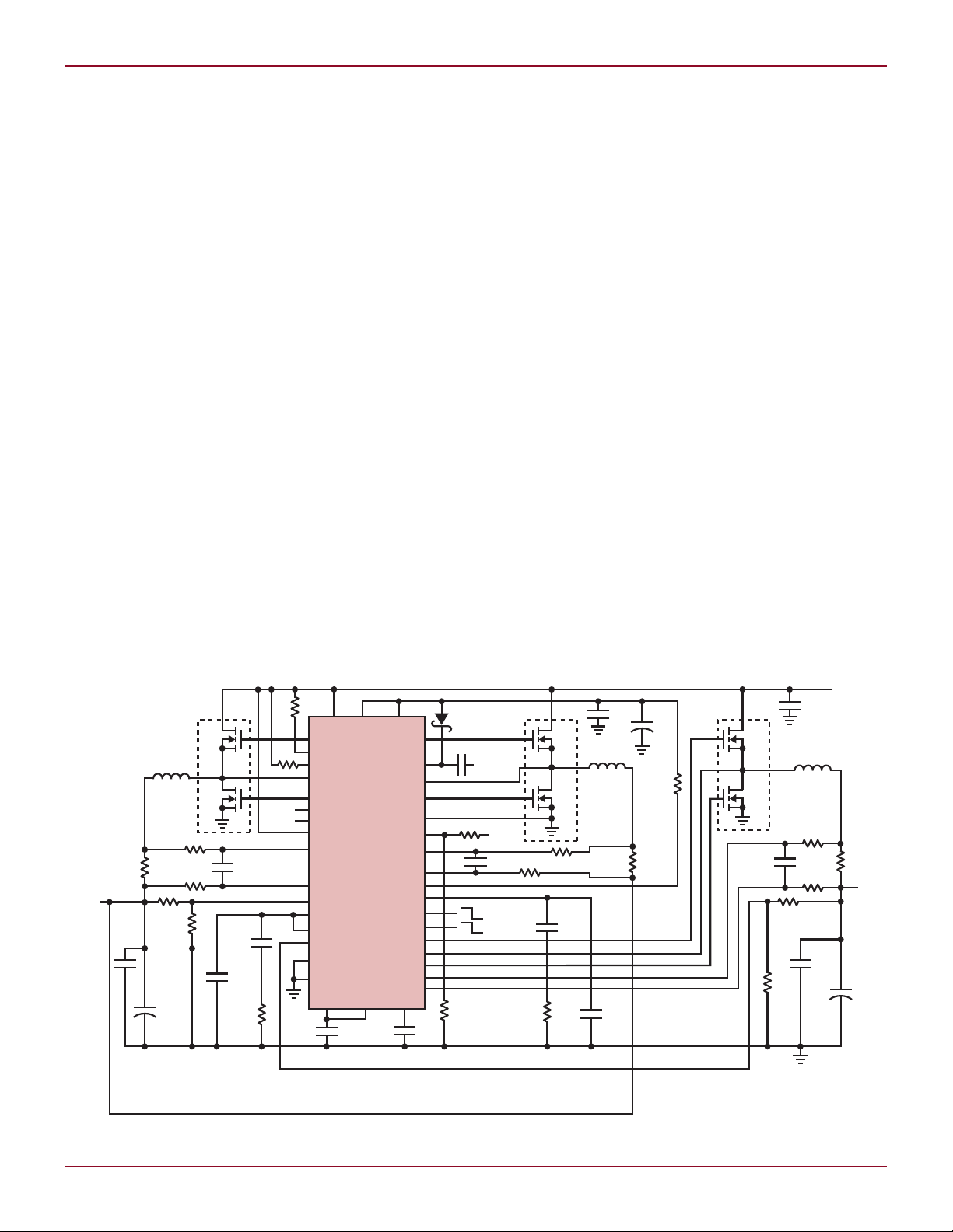
Figure 1 shows a 2-output converter
working from a 14V to 24V input.
Channels 1 and 2 feed the same 1.8V
output, while channel 3 controls a
second 12V output. This 2 + 1 mode
requires just one RUN pin (RUN1) to
enable both channels 1 and 2. The
error amp of channel 2 is disabled
and both channels share channel 1’s
feedback divider. Post package trimming of the current sense comparators
provides excellent current sharing
between channels 1 and 2, as the load
step of Figure 2 shows. Channels 1 and
2 run 180° out of phase to minimize
the output ripple on their 2-phase
single output. A minimum on-time of
<90 nanoseconds allows low duty cycle
operation even at high frequencies—at
24VIN to 1.8V
, this 500kHz regula-
OUT
tor never misses a pulse.
The EXTVCC pin can be connected
to a 5V supply to power the internal
MOSFET drivers and control circuits.
An internal switch connects EXTVCC to
INTV
with a typical voltage drop of
CC
just 50mV. If EXTVCC is not connected,
the LTC3853’s internal regulator uses
the main input supply, VIN, to provide
5V to the internal circuitry and drivers
at INTVCC. In either case, the switching
frequency is set with a divider from
the predictable 5V at INTVCC, with
1.2V at the FREQ pin corresponding
to free-running 500kHz. If an external
frequency source is available, a phase
locked loop enables the LTC3853 to
Figure 1. For applications that need up to 30A of current, channels 1 and 2 of the LTC3853 can be combined to share the load for a single output.
The two channels operate 180º out of phase to minimize output ripple. Channel 3’s high common mode range allows it to provide 12V.
40
40
Linear Technology Magazine • June 2008
POWER LOSS (mW)
EFFICIENCY (%)
LOAD CURRENT (A)
100.1
100
0
10k
100
1
1k
10
20
30
40
50
60
70
80
90
VIN = 24V
V
OUT3
= 12V
2+1 MODE
EFFICIENCY
POWER LOSS
CONTINUOUS MODE
PULSE-SKIPPING MODE
BURST MODE OPERATION
V
OUT1,2
200mV/DIV
I
L2
2A/DIV
I
L1
2A/DIV
25µs/DIV
VIN = 14V
V
OUT1,2
(NOM) = 1.8V
LOAD STEP ON V
OUT1,2
= 1A TO 6A
Figure 2. Post-package trimming of the
LTC3853’s current sense comparators
provides excellent current sharing between
channels 1 and 2, even during a transient.
sync with frequencies between 250kHz
and 750kHz.
The LTC3853 can be set to operate
in one of three modes under light load
conditions. Burst Mode operation offers the highest light load efficiency by
switching in a “burst” of one to several
pulses replenishing the charge stored
in the output capacitors, followed by a
long sleep period when the load current
is supplied by the output capacitors.
Forced continuous mode offers fixed
frequency operation from no load to
full load, providing the lowest output
voltage ripple at the cost of light load
efficiency. Pulse-skipping mode operates by preventing inductor current
reversal by turning off the synchronous switch as needed. This mode
is a compromise between the other
two modes, offering lower ripple than
Burst Mode operation and better light
load efficiency than forced continuous
mode. Regardless of the mode selected,
the LTC3853 operates in constant frequency mode at higher load currents.
Figure 3 shows the efficiency in each
of the three modes.
Each of the LTC3853’s channels
can be enabled with its own RUN
pin, or slewed up or down with its
own TRACK/SS pin. Tracking holds
the feedback voltage to the lesser of
the internal reference voltage or the
voltage on TRACK/SS, which can be
brought up with an external ramp or
with its own 1.2µA internal current
source. With all of the TRACK/SS
pins held low and any output enabled
through its RUN pin, the 5V INTVCC is
still available for ancillary keep-alive
circuits.
Pulse-skipping mode is always
enabled at start-up to prevent sinking current from a pre-biased output
voltage. When the output reaches 80%
of the set value, the part switches over
to forced continuous mode until the
output has entered the POWER GOOD
window, at which point it switches
over to the selected mode of operation. Forced continuous mode reduces
the output ripple as the power good
threshold is crossed, to ensure that
the POWER GOOD indicators make
just one low to high transition.
Three different max current comparator sense thresholds can be set
via the ILIM pin. The current is sensed
using a high speed rail-to-rail differential current sense comparator. The
circuit of Figure 1 uses accurate sense
resistors between the inductors and
the outputs. For reduced power loss at
high load currents, the LTC3853 can
also monitor the parasitic resistance
of the inductor (DCR sensing). Peak
inductor current is limited on a cycleby-cycle basis and is independent
of duty cycle. If load current is high
enough to cause the feedback voltage
DESIGN IDEAS L
Figure 3. Efficiency for channel 3 in Figure 1—
in each of the three modes of operation
to drop, current limit fold back protects
the power components by reducing the
current limit. For predictable tracking,
current limit fold back is disabled
during start-up. Input undervoltage
lockout, output overvoltage shutdown
and thermal shutdown also protect
the power components and the IC
from damage.
Conclusion
The LTC3853’s small footprint belies
its versatility and extensive feature
set. From inputs up to 24V it can
regulate three separate outputs, or it
can be configured for higher currents
by tying channels 1 and 2 together.
Either way, the phase relationship
between channels is automatically
optimized to reduce ripple currents.
At low duty cycles, the short minimum
on-time ensures constant frequency
operation, and peak current limit
remains constant even as duty cycle
changes. The cost-effective LTC3853
incorporates these features, and
more, into a 40-pin 6mm × 6mm QFN
package.
L
LT3570, continued from page 29
DSL Modem
Figure 4 shows an application for a
DSL modem or set-top box. The supply voltage for V
adapter that can range from 8V to 30V.
IN2
comes from a wall
This voltage is stepped down to 5V at
100mA for V
the power to drive both the boost
regulator and LDO controller. V
is set to 8V at 200mA and V
Linear Technology Magazine • June 2008
, which then supplies
OUT2
OUT3
is set
OUT1
to 3.3V at 500mA. Figure 5 shows the
load step response of V
with a 200mA load step on V
OUT1
and V
OUT1
Conclusion
The LT3570 is a monolithic dual
output switching regulator (buck and
boost) with a NPN LDO controller and
is ideal for a broad variety of applications. Because the LT3570 offers a high
OUT2
.
level of system integration, it greatly
simplifies board design for complex
applications that need multiple voltage supply rails. With the flexibility of
independent supply inputs and adjustable frequency, the user can set a wide
array of custom output voltages. The
LT3570 is a feature rich solution that
satisfies the needs for multiple output
voltages in a compact solution.
L
4141
 Loading...