

L DESIGN FEATURES
MODE/PLLIN
FREQ/PLLFLTR
RUN
TK/SS
I
TH
V
FB
SENSE
–
SENSE
+
V
IN
TG
BOOST
SW
INTV
CC
BG
GND
I
LIM
LTC3851
0.1µF
0.047µF
0.1µF
330pF
2200pF
R
FREQ
82.5k
15k
V
OUT
3.3V
15A
47pF
+
4.7µF
+
C
OUT
330µF
s2
C
IN
22µF
HAT2170H
HAT2170H
C
OUT
: SANYO 6TPE330MIL
CIN: SANYO 63HVH22M
L1: VISHAY IHLP5050-EZERR68M01
CMDSH05-4
154k
1%
48.7k
1%
V
IN
4.5V TO 32V
L1
0.68µH
3.01k
0.1µF
30.1k
R
FREQ
(k)
10
100
OSCILLATOR FREQUENCY (kHz)
500
250
750
1000
36 60 160 1000
Synchronous Buck Controller in
3mm × 3mm QFN Fits Automotive
and Industrial Applications with
4V–38V Input Capability
Introduction
The LTC3851 is a versatile synchronous step-down switching regulator
controller that is available in a space
saving 16-lead 3mm × 3mm QFN or
convenient narrow SSOP packages. Its
wide input range of 4V to 38V makes it
well-suited for regulating power from a
variety of sources, including automotive batteries, 24V industrial supplies
and unregulated wall transformers.
The strong onboard drivers allow the
use of high power external MOSFETs
to produce output currents up to 20A
with output voltages ranging from
0.8V to 5.5V.
The constant frequency peak cur-
rent mode control architecture provides
excellent line and load regulation along
with load current sharing capability
and dependable cycle-by-cycle current
limiting. OPTI-LOOP® compensation
simplifies loop stability design and
provides well-behaved regulation over
a broad range of operating conditions.
The LTC3851 has ±1% output voltage
tolerance over temperature. The part’s
low minimum on-time (90ns, typical)
allows for low duty cycle operation
even with switching frequencies as
high as 750kHz.
Two Current Sensing Options
The LTC3851 features a high input
impedance current sense comparator.
This allows the use of the inductor’s
DC resistance (DCR) as the current
sense element in conjunction with an
RC filter. DCR current sensing allows
the designer to eliminate the need for a
discrete sense resistor, thereby maximizing efficiency and lowering solution
cost. Alternately, higher current sense
accuracy may be achieved by connecting the SENSE+ and SENSE– pins to a
precision sense resistor in series with
the inductor. The LTC3851 offers the
choice of three pin-selectable maximum current sense thresholds (30mV,
by Mark Mercer
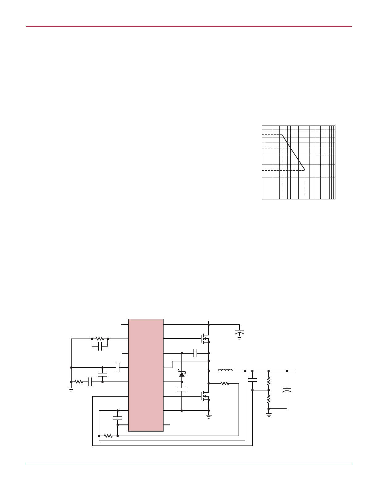
Figure 1. Relationship between oscillator
frequency and resistor connected between
FREQ/PLLFLTR and GND
50mV and 75mV) to accommodate a
wide range of DCR values and output
current levels.
As with all constant frequency,
peak current mode control switching
regulators, the LTC3851 utilizes slope
compensation to prevent sub-harmonic oscillations at high duty cycles. This
16
Figure 2. High efficiency 3.3V/15A power supply with DCR sensing
Linear Technology Magazine • September 2008
DESIGN FEATURES L
EFFICIENCY (%)
LOAD CURRENT (A)
1000.01
100
0
0.1 1 10
10
20
30
40
50
60
70
80
90
Burst Mode
OPERATION
CONTINUOUS
CONDUCTION MODE
PULSE-
SKIPPING
MODE
VIN = 12V
V
OUT
= 3.3V
MODE/PLLIN
FREQ/PLLFLTR
RUN
TK/SS
I
TH
V
FB
SENSE
–
SENSE
+
V
IN
TG
BOOST
SW
INTV
CC
BG
GND
I
LIM
LTC3851
0.1µF
0.1µF
100pF
1000pF
0.01µF
PLLIN
350kHz
1000pF
10k
10Ω
10Ω
7.5k
R
SENSE
0.002Ω
V
OUT
1.5V
15A
1000pF
+
4.7µF
+
C
OUT
330µF
s2
C
IN
180µF
33pF
RJK0305DPB
RJK0301DPB
C
OUT
: SANYO 2R5TPE330M9
L1: SUMIDA CEP125-OR6MC
CMDSH-3
42.2k
1%
48.7k
1%
V
IN
6V TO 14V
L1
0.68µH
is accomplished internally by adding
a compensating ramp to the inductor
current signal. Normally, this results
in a >40% reduction of maximum
inductor peak current at high duty
cycles. However, the LTC3851 uses
a novel scheme that allows the maximum peak inductor current to remain
stable throughout all duty cycles.
Versatility
During heavy load operation, the
LTC3851 operates in constant frequency, continuous conduction mode.
At light loads, it can be configured
to operate in high efficiency Burst
Mode® operation, constant frequency
pulse-skipping mode or forced continuous conduction mode. Burst Mode
operation offers the highest efficiency
because energy is transferred from the
input to the output in pulse trains
of one to several cycles. During the
intervening period between pulse
trains, the top and bottom MOSFETs
are turned off and only the output
capacitor provides current to the load.
Forced continuous conduction mode
results in the lowest output voltage
ripple, but is the least efficient at light
loads. Pulse-skipping mode offers
a compromise—lower output ripple
than Burst Mode operation and more
efficiency than continuous conduction mode.
Figure 3. Efficiency vs load current with three
modes of operation for the circuit of Figure 2
The switching frequency of the
LTC3851 may be programmed from
250kHz to 750kHz by the resistor,
R
, connected to the FREQ/PLL-
FREQ
FLTR pin. This provides the flexibility
needed to optimize efficiency. Figure 1
shows a plot of the switching frequency
vs R
. Additionally, the switching
FREQ
frequency may be synchronized to
an external clock. While doing so,
the LTC3851 will operate in forced
continuous conduction mode.
The output voltage can be ramped
during start-up by means of an adjustable soft-start function, or it can
track an external ramp signal. Track
and soft-start control are combined in
a single pin, TK/SS. Whenever TK/SS
is less than 0.64V, the LTC3851 operates in pulse-skipping mode. This
feature allows for starting up into a
pre-biased load. When TK/SS is between 0.64V and 0.74V, the regulator
operates in forced continuous mode
to ensure a smooth transition from
start-up to steady state. Once TK/SS
exceeds 0.74V, the mode of operation is determined by the state of the
MODE/PLLIN pin.
The RUN pin enables or disables
the LTC3851. This pin has a precision
1.22V turn-on threshold which is useful for power supply sequencing. The
turn-off threshold is 1.10V. There is
an internal 2µA pull-up current source
on the RUN pin.
The LTC3851’s fault protection
features include foldback current
limiting, output overvoltage detection
and input undervoltage detection. If
an overload event causes the output
to fall to less than 40% of the target
regulation value, then the LTC3851
folds back the maximum current sense
threshold. This reduces the on-time in
order to minimize power dissipation in
the top MOSFET. If the output voltage
is more than 10% above the target
regulation value, the bottom MOSFET
turns on until the output falls back
into regulation. If the input voltage is
allowed to fall low enough such than
the output of the internal linear regulator falls below 3.2V, then switching
operation is disabled. This feature
continued on page 36
Linear Technology Magazine • September 2008
Figure 4. High efficiency 1.5V/15A power supply synchronized to 350kHz
17

L DESIGN IDEAS
BATTERY VOLTAGE (V)
2.7
EFFICIENCY (%)
80
90
3.9
70
60
3
3.3
3.5
4.2
100
R
CLPROG
= 3.01K
R
PROG
= 1K
I
VOUT
= 0mA
5x CHARGING EFFICIENCY
1x CHARGING EFFICIENCY
10µH
VOUT3
CAP3
IFB3
LT3587
8.06k
R
IFB3
EN/SS3
SW3
VIN
1µF
V
VIN
2.5V TO 5V
V
DAC-OUT
DAC
LTC2630
PWM
FREQ
2.5V
0V
MN1
Si1304BDL
IR05H40CSPTR
Figure 3. Battery charging efficiency vs
battery voltage with no external load
(P
should be pulled-up to the same voltage. In Figure 2 the LDO3V3 regulator
is used as the pull-up voltage for the
FAULT signal and the power supply
for the low power microcontroller
used to process pushbutton events
and sequence the power supplies.
The FAULT pin also acts as an input
and hence, must be high before any
outputs are enabled.
Compact LED Driver
The LT3587 LED driver is designed
to drive up to six LEDs with average
LED currents between 20mA and 1µA.
When the LT3587’s V
a current regulated LED driver, the
V
FB3
protection function. By connecting a
resistor between V
device limits the maximum allowable
output voltage on V
is extremely important in LED applications because without it the client
device may be damaged if one of the
LEDs were to open; in such a case,
the output would continue to rise as
)
BAT/PBUS
is used as
OUT3
pin can be used as an overvoltage
and V
OUT
. This feature
OUT3
FB3
the
Figure 4. Six white LED driver with PWM and analog dimming
the current regulation loop increases
voltage in an attempt to regulate the
current.
The integrated LED driver in the
LT3587 is capable of accepting a direct
PWM dimming signal into its enable
input (EN/SS3) and/or accommodates
analog dimming via an external DAC.
See Figure 4 for a partial application
circuit showing the LED driver with
direct PWM and analog dimming.
LEDs can change color when the
current through them changes, but
PWM dimming maintains color consistency over the dimming range, as the
ON part of the PWM cycle is always the
same current. In PWM dimming, the
brightness of the LEDs is a function of
average current, adjusted by changing
the duty cycle of the PWM signal. In
analog dimming, the constant current
through the LEDs is adjusted, which
causes variations in color.
The LT3587 accepts PWM signals
with frequencies over 60Hz to assure
flicker-free operation. High PWM frequencies are achievable because of
the internal disconnect FET between
CAP3 and V
. This FET ensures
OUT3
that CAP3 maintains its steady-state
value while the PWM signal is low,
resulting in minimal startup delays.
For a 100Hz PWM dimming signal and
allowing for 10% deviation from linearity at the lowest duty cycle, the LT3587
allows for a dimming ratio of 30:1. If
the maximum amount of adjustment
range is desired, an external DAC,
such as the LTC2630, can be used to
feed an adjustment voltage onto the
IFB3 resistor, creating an LED current
range of 20,000:1.
Conclusion
Two highly integrated devices, the
LTC3586 and LT3587 can be combined
to create a complete USB compatible
power solution for portable cameras
and other feature-rich portable devices. The solution is robust, high
performance and compact, with efficient battery charging, instant-on
capability and LED protection.
L
LTC3851, continued from page 17
protects against insufficient turn-on
voltage for the top MOSFET.
3.3V/15A Regulator with
DCR Sensing
Figure 2 shows a 400kHz, 3.3V output
regulator using DCR current sensing.
The DC resistance of the inductor is
used as the current sense element,
eliminating the need for a discrete
sense resistor and thus maximizing
efficiency. Figure 3 shows a plot of the
36
36
efficiency vs load for all three modes
of operation with an input voltage of
12V.
1.5V/15A Regulator
Synchronized at 350kHz
Figure 4 illustrates a 1.5V output
regulator that is synchronized to
an external clock. The loop filter
components connected to the FREQ/
PLLFLTR pin are optimized to achieve
a jitter free oscillator frequency and
reduced lock time.
Conclusion
The LTC3851 combines high performance, ease of use and a comprehensive
feature set in a 3mm × 3mm 16-pin
package. DCR current sensing and
Burst Mode® operation keep efficiency
high. With a broad 4V to 38V input
range, strong MOSFET drivers, low
minimum on-time and tracking, the
LTC3851 is ideal for automotive electronics, server farms, datacom and
telecom power supply systems and
industrial equipment.
Linear Technology Magazine • September 2008
L
 Loading...