

advertisement
y
80µA Quiescent Current Synchronous Step-Down Controller Extends Battery Life in Automotive Applications – Design Note 1014
Julian Zhu
Introduction
Battery powered applications that have a signifi cant
amount of time in st andby mode, require electric al circuits
to operate with a low quiescent current to preserve battery life. The LTC3835 synchronous step-down controller
is an excellent solution with its ultralow quiescent current (80µA). Other features make it uniquely qualifi ed to
satisfy the needs of automotive applications. A wide 4V
to 36V input voltage range protects the supply against
high input voltage transients and is compatible with low
voltage cold crank conditions. The constant frequency
current-mode architecture with high-side inductor current sensing provides excellent line and load regulation
and reliable current limiting and sharing. The 0.8V to
10V output voltage range provides fl exibility for a variety
of applications. Solution size is small due to the 650kHz
switching frequency, which reduces external component
sizes, and the integrated synchronous FET driver, which
keeps component count low. Furthermore, the LTC3835
provides high effi ciency over a wide load range up to 20A.
Other important features include:
0.1µF
68.1k
215k
39pF
1200pF
10k
150pF
1nF
CLKOUT
PLLLPF
RUN
PGOOD
TRACK/SS
I
TH
LTC3835
SGND
PLLIN/MODE
V
FB
–
SENSE
+
SENSE
BOOST
INTV
EXTV
PGND
V
TG
SW
BG
IN
CC
CC
• The output voltage can be ramped during start-up with
an adjustable soft-start or it can track an external ramp
signal.
• The controller can be synchronized to an external clock
via a phase-locked loop.
• The CLKOUT pin and current mode control allow interleaved operation of multiple parallel controllers for
delivery of high output current with accurate current
sharing.
The LTC3835 has overvoltage and overcurrent (shortcircuit) protection, a power good monitor and an EXTV
option for improved effi ciency when V
> 4.7V. All
OUT
CC
these are packed in a small 20-pin exposed pad TSSOP or
4mm × 5mm QFN package. The LTC3835-1 fi ts in a smaller
16-pin SSOP package or 5mm × 3mm DFN package,
by eliminating CLKOUT, EXTV
and the power good
CC
indicator.
, LT, LTC, LTM and Burst Mode are registered trademarks of Linear Technolog
Corporation. All other trademarks are the property of their respective owners.
V
IN
+
4V TO 36V
V
OUT
3.3V
5A
C
OUT
150µF
10V
0.22µF
CMDSH-4
4.7µF
Si4840DY
3.3µH
Si4840DY
0.012Ω
10µF
50V
CERAMIC
12/06/1014
L: SUMIDA, CDEP105-3R2MC-88
C
: SANYO, 10TPD150M
OUT
DN1014 F01
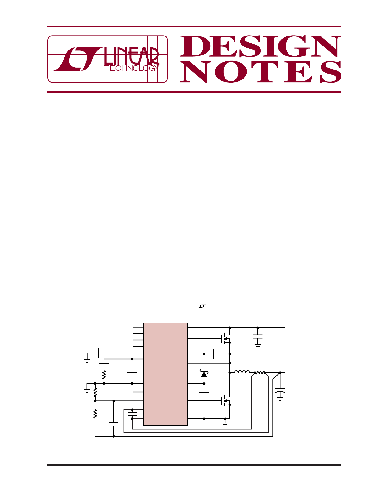
Figure 1. High Effi ciency Synchronous Step-Down Converter Consumes only 80µA in Standby Mode
High Effi ciency at Standby
The LTC3835 uses synchronous rectifi cation and N-channel MOSFETs to achieve high effi ciency over a wide load
range. At light load it minimizes the IC supply current with
®
Burst Mode
operation, where the controller switches in
fi xed duty cycle bursts, as needed, to reduce the IC supply current. When the load current is extremely low, the
controller enters sleep mode by turning off both external
MOSFETs and most of its internal circuitry, further reduc-
DN1014 F02
100000
10000
POWER LOSS (mW)
1000
100
10
1
0.1
100
90
80
70
60
50
40
EFFICIENCY (%)
30
20
10
0
0.01 0.1 1 10 100 1000 10000
0.001
EFFICIENCY
= 12V; V
V
IN
LOAD CURRENT (mA)
= 3.3V
OUT
POWER LOSS
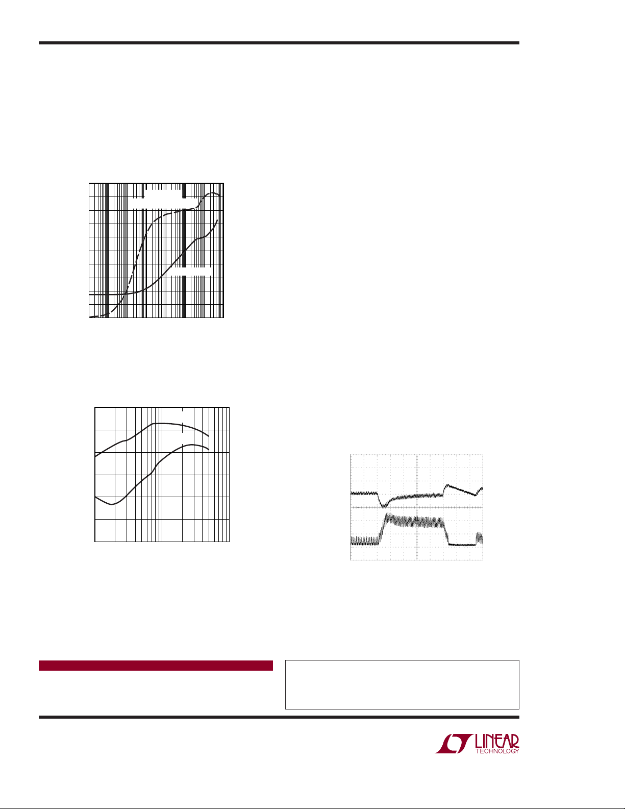
Figure 2. Effi ciency and Power Loss vs
Load Current for the Circuit in Figure 1.
100
95
90
VIN = 4V
VIN = 12V
ing quiescent current. To maximize effi ciency during Burst
Mode operation the bottom MOSFET is turned off when
the instantaneous inductor current is close to zero. The
IC is also designed with an EXTV
pin to further increase
CC
conversion effi ciency.
3.3V/5A Synchronous DC/DC Converter
Figure 1 shows an automotive application that converts a
4V to 36V input to a 3.3V/5A output. As Figure 2 shows,
the converter achieves high effi ciency, up to 92%, at
12V input and maintains light-load effi ciency, above
65%, down to 1mA load current. The no-load IC supply
quiescent current is kept below 80µA. For low dropout
operation the effi ciency can reach 96.5% at 4V input as
illustrated in Figure 3.
The controller us es OPTI-LOOP compensation to opt imize
the transient response and thus minimize the output
capacitance. Figure 4 shows the transient response for
the circuit in Figure 1.
Conclusion
The LTC3835 contro ller is especially well suited to automo tive and other battery-powered applications that demand
low quiescent current and light-load effi ciency—important for preserving battery life in applications that spend
signifi cant time in standby. The LTC3835 also offers a
wide input and output voltage range and many other
advanced features in either leaded or leadless thermally
effi cient packages.
85
EFFICIENCY (%)
80
75
70
0.1
110
LOAD CURRENT (A)
DN1014 F03
Figure 3. Effi ciency vs Load Current at VIN = 4V
and VIN = 12V for the Circuit in Figure 1.
Data Sheet Download
www.linear.com
Linear Technology Corporation
1630 McCarthy Blvd., Milpitas, CA 95035-7417
(408) 432-1900
●
FAX: (408) 434-0507 ● www.linear.com
V
OUT
100mV/
DIV AC
COUPLED
I
L
2A/DIV
20µs/DIV
DN1014 F04
Figure 4. Load Step Transient with
12V Input for the Circuit in Figure 1.
For applications help,
call (408) 432-1900, Ext. 3598
dn1014f LT 1206 • PRINTED IN THE USA
© LINEAR TECHNOLOGY CORPORATION 2006
 Loading...