

FEATURES
LTC3830/LTC3830-1
High Power Step-Down
Synchronous DC/DC Controllers
for Low Voltage Operation
U
DESCRIPTIO
■
High Power Switching Regulator Controller
for 3.3V-5V to 1.xV-3.xV Step-Down Applications
■
No Current Sense Resistor Required
■
Low Input Supply Voltage Range: 3V to 8V
■
Maximum Duty Cycle >91% Over Temperature
■
All N-Channel External MOSFETs
■
Excellent Output Regulation: ±1% Over Line, Load
and Temperature Variations
■
High Efficiency: Over 95% Possible
■
Adjustable or Fixed 3.3V Output (16-Pin Version)
■
Programmable Fixed Frequency Operation: 100kHz to
500kHz
■
External Clock Synchronization
■
Soft-Start (16-Pin Version and LTC3830-1)
■
Low Shutdown Current: <10µA
■
Overtemperature Protection
■
Available in S8, S16 and SSOP-16 Packages
U
APPLICATIO S
■
CPU Power Supplies
■
Multiple Logic Supply Generator
■
Distributed Power Applications
■
High Efficiency Power Conversion
The LTC®3830/LTC3830-1 are high power, high efficiency switching regulator controllers optimized for
3.3V-5V to 1.xV-3.xV step-down applications. A precision internal reference and feedback system provide
±1% output regulation over temperature, load current
and line voltage variations. The LTC3830/LTC3830-1 use
a synchronous switching architecture with N-channel
MOSFETs. Additionally, the chip senses output current
through the drain-source resistance of the upper
N-channel FET, providing an adjustable current limit
without a current sense resistor.
The LTC3830/LTC3830-1 operate with an input supply
voltage as low as 3V and with a maximum duty cycle of
>91% over temperature. They include a fixed frequency
PWM oscillator for low output ripple operation. The 200kHz
free-running clock frequency can be externally adjusted or
synchronized with an external signal from 100kHz to 500kHz.
In shutdown mode, the LTC3830 supply current drops to
<10µA. The LTC3830-1 differs from the LTC3830 S8 ver-
sion by replacing shutdown with a soft-start function.
For a similar, pin compatible DC/DC converter with an
output voltage as low as 0.6V, please refer to the LTC3832.
, LTC and LT are registered trademarks of Linear Technology Corporation.
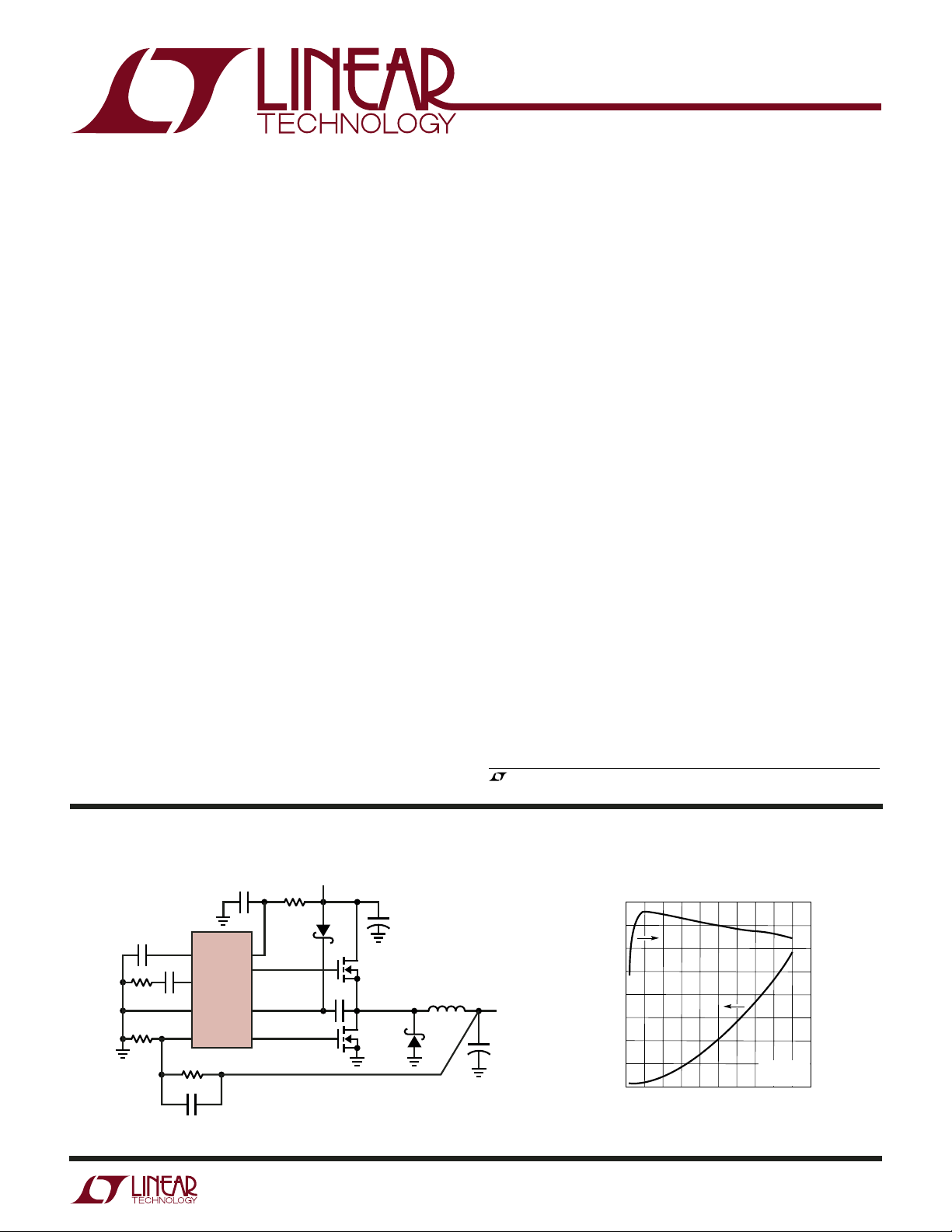
TYPICAL APPLICATIO
4.7µF
0.1µF
15k
12.7k 1%
0.01µF
SS
COMP
GND
FB
5.36k 1%
3.3nF
LTC3830-1
PV
CC2
G1
PV
CC1
G2
L: SUMIDA CDEP105-3R2MC-88
C
Figure 1. High Efficiency 3V-6V to 1.8V Power Converter
5.1Ω
MBR0520T1
: PANASONIC EEFUEOD271R
OUT
U
V
IN
3V TO 6V
0.1µF
+
M1
Si7806DN
M2
Si7806DN
220µF
10V
L
3.2µH
B320A
Efficiency and Power Loss vs Load Current
4.0
3.5
3.0
2.5
1.8V
9A
+
C
OUT
270µF
2V
3830 F01
2.0
1.5
POWER LOSS (W)
1.0
0.5
0
0
LOAD CURRENT (A)
VIN = 3.3V
V
OUT
100
90
80
EFFICIENCY (%)
70
60
50
40
30
= 1.8V
20
87654321910
3830 TA02
3830fa
1
LTC3830/LTC3830-1
WWWU
ABSOLUTE AXI U RATI GS
(Note 1)
Supply Voltage
VCC....................................................................... 9V
PV
................................................................ 14V
CC1,2
Input Voltage
IFB, I
............................................... –0.3V to 14V
MAX
SENSE+, SENSE–, FB,
SHDN, FREQSET ....................... –0.3V to V
UU
W
+ 0.3V
CC
PACKAGE/ORDER I FOR ATIO
ORDER PART
NUMBER
LTC3830ES8
S8
PART MARKING
3830
ORDER PART
NUMBER
LTC3830-1ES8
S8
PART MARKING
38301
G1
1
PV
2
CC1
GND
3
FB
4
8-LEAD PLASTIC SO
T
= 125°C, θJA = 130°C/ W
JMAX
G1
1
PV
2
CC1
GND
3
FB
4
8-LEAD PLASTIC SO
T
= 125°C, θJA = 130°C/ W
JMAX
TOP VIEW
S8 PACKAGE
TOP VIEW
S8 PACKAGE
8
G2
V
/PV
7
CC
CC2
COMP
6
SHDN
5
8
G2
/PV
V
7
CC
CC2
COMP
6
SS
5
Junction Temperature (Note 11)........................... 125°C
Operating Temperature Range (Note 9) .. – 40°C to 85°C
Storage Temperature Range ................. –65°C to 150°C
Lead Temperature (Soldering, 10 sec)..................300°C
ORDER PART
NUMBER
TOP VIEW
1
G1
2
PV
CC1
3
PGND
4
GND
–
SENSE
SENSE
16-LEAD PLASTIC SSOP
5
6
FB
+
7
8
SHDN
GN PACKAGE
T
= 125°C, θJA = 130°C/ W (GN)
JMAX
= 125°C, θJA = 100°C/ W (S)
T
JMAX
G2
16
PV
15
CC2
V
14
CC
I
13
FB
I
12
MAX
FREQSET
11
COMP
10
SS
9
S PACKAGE
16-LEAD PLASTIC SO
LTC3830EGN
LTC3830ES
GN PART
MARKING
3830
Consult LTC Marketing for parts specified with wider operating temperature ranges.
ELECTRICAL CHARACTERISTICS
range, otherwise specifications are at TA = 25°C. VCC, PV
The ● denotes specifications that apply over the full operating temperature
, PV
CC1
= 5V, unless otherwise noted. (Note 2)
CC2
SYMBOL PARAMETER CONDITIONS MIN TYP MAX UNITS
V
PV
V
V
V
∆V
CC
CC
UVLO
FB
OUT
OUT
Supply Voltage ● 358 V
PV
, PV
CC1
Voltage (Note 7) ● 3 13.2 V
CC2
Undervoltage Lockout Voltage 2.4 2.9 V
Feedback Voltage V
Output Voltage V
Output Load Regulation I
Output Line Regulation V
= 1.25V 1.255 1.265 1.275 V
COMP
= 1.25V 3.250 3.3 3.350 V
COMP
= 0A to 10A (Note 6) 2 mV
OUT
= 4.75V to 5.25V 0.1 mV
CC
● 1.252 1.265 1.278 V
● 3.235 3.3 3.365 V
3830fa
2
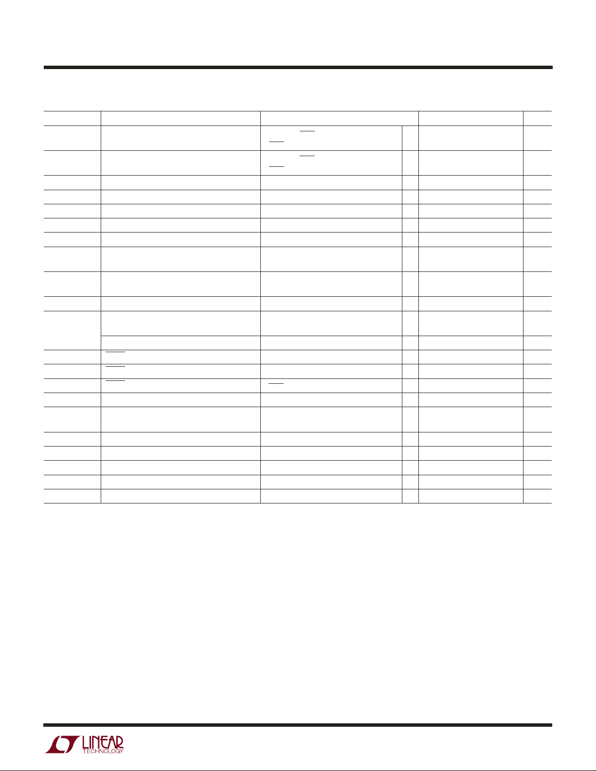
LTC3830/LTC3830-1
ELECTRICAL CHARACTERISTICS
range, otherwise specifications are at TA = 25°C. VCC, PV
The ● denotes specifications that apply over the full operating temperature
, PV
CC1
= 5V, unless otherwise noted. (Note 2)
CC2
SYMBOL PARAMETER CONDITIONS MIN TYP MAX UNITS
I
VCC
I
PVCC
f
OSC
V
SAWL
V
SAWH
V
COMPMAX
∆f
/∆I
OSC
FREQSET
A
V
g
m
I
COMP
I
MAX
V
IH
V
IL
I
IN
I
SS
I
SSIL
R
SENSE
R
SENSEFB
tr, t
f
t
NOV
DC
MAX
Note 1: Absolute Maximum Ratings are those values beyond which the life
of a device may be impaired.
Note 2: All currents into device pins are positive; all currents out of device
pins are negative. All voltages are referenced to ground unless otherwise
specified.
Note 3: Supply current in normal operation is dominated by the current
needed to charge and discharge the external FET gates. This will vary with
the LTC3830 operating frequency, operating voltage and the external FETs
used.
Note 4: The open-loop DC gain and transconductance from the SENSE
and SENSE– pins to COMP pin will be (AV)(1.265/3.3) and (gm)(1.265/3.3)
respectively.
Note 5: Rise and fall times are measured using 10% and 90% levels. Duty
cycle and nonoverlap times are measured using 50% levels.
Note 6: Guaranteed by design, not subject to test.
Note 7: PV
at 95% maximum duty cycle and for the current limit protection circuit to
Supply Current Figure 2, V
V
= 0V ● 110 µA
SHDN
PVCC Supply Current Figure 2, V
= 0V ● 0.1 10 µA
V
SHDN
= V
SHDN
SHDN
CC
= VCC (Note 3) ● 14 20 mA
● 0.7 1.6 mA
Internal Oscillator Frequency FREQSET Floating ● 160 200 250 kHz
V
at Minimum Duty Cycle 1.2 V
COMP
V
at Maximum Duty Cycle 2.2 V
COMP
Maximum V
COMP
VFB = 0V, PV
= 8V 2.85 V
CC1
Frequency Adjustment 10 kHz/µA
Error Amplifier Open-Loop DC Gain Measured from FB to COMP, ● 46 55 dB
Error Amplifier Transconductance Measured from FB to COMP, ● 520 650 780 µmho
+
SENSE
and SENSE– Floating, (Note 4)
+
and SENSE– Floating, (Note 4)
SENSE
Error Amplifier Output Sink/Source Current 100 µA
I
Sink Current V
MAX
I
Sink Current Tempco V
MAX
= V
IMAX
CC
(Note 10)
= VCC (Note 6) 3300 ppm/°C
IMAX
91215 µA
● 41220 µA
SHDN Input High Voltage ● 2.4 V
SHDN Input Low Voltage ● 0.8 V
SHDN Input Current V
Soft-Start Source Current VSS = 0V, V
Maximum Soft-Start Sink Current V
In Current Limit V
= V
SHDN
CC
= 0V, V
IMAX
= VCC, V
IMAX
= VCC (Note 8), PV
SS
IFB
● 0.1 1 µA
IFB
= V
CC
● –8 –12 –16 µA
= 0V, 1.6 mA
= 8V
CC1
SENSE Input Resistance 29.2 kΩ
SENSE to FB Resistance 18 kΩ
Driver Rise/Fall Time Figure 3, PV
Driver Nonoverlap Time Figure 3, PV
Maximum G1 Duty Cycle Figure 3, VFB = 0V (Note 5), PV
CC1
CC1
= PV
= 5V (Note 5) ● 80 250 ns
CC2
= PV
= 5V (Note 5) ● 25 120 250 ns
CC2
= 8V ● 91 95 %
CC1
Note 8: The current limiting amplifier can sink but cannot source current.
Under normal (not current limited) operation, the output current will be
zero.
Note 9: The LTC3830E/LTC3830-1E are guaranteed to meet performance
specifications from 0°C to 70°C. Specifications over the –40°C to 85°C
operating temperature range are assured by design, characterization and
correlation with statistical process controls.
Note 10: The minimum and maximum limits for I
over temperature
MAX
includes the intentional temperature coefficient of 3300ppm/°C. This
+
induced temperature coefficient counteracts the typical temperature
coefficient of the external power MOSFET on-resistance. This results in a
relatively flat current limit over temperature for the application.
Note 11: This IC includes overtemperature protection that is intended to
protect the device during momentary overload conditions. Junction
temperature will exceed 125°C when overtemperature protection is active.
must be higher than VCC by at least 2.5V for G1 to operate
CC1
Continuous operation above the specified maximum operating temperature
may impair device reliability.
be active.
3830fa
3
LTC3830/LTC3830-1
TEMPERATURE (˚C)
–50
ERROR AMPLIFIER TRANSCONDUCTANCE (µmho)
700
750
800
25 75
3830 G05
650
600
–25 0
50 100 125
550
500
TEMPERATURE (°C)
–50
40
ERROR AMPLIFIER OPEN-LOOP GAIN (dB)
45
50
55
60
–25 0 25 50
2830 G07
75 100 125
EXTERNAL SYNC FREQUENCY (kHz)
100
0.5
V
SAWH
– V
SAWL
(V)
0.6
0.8
0.9
1.0
1.5
1.2
200
300
3830 G10
0.7
1.3
1.4
1.1
400
500
TA = 25°C
UW
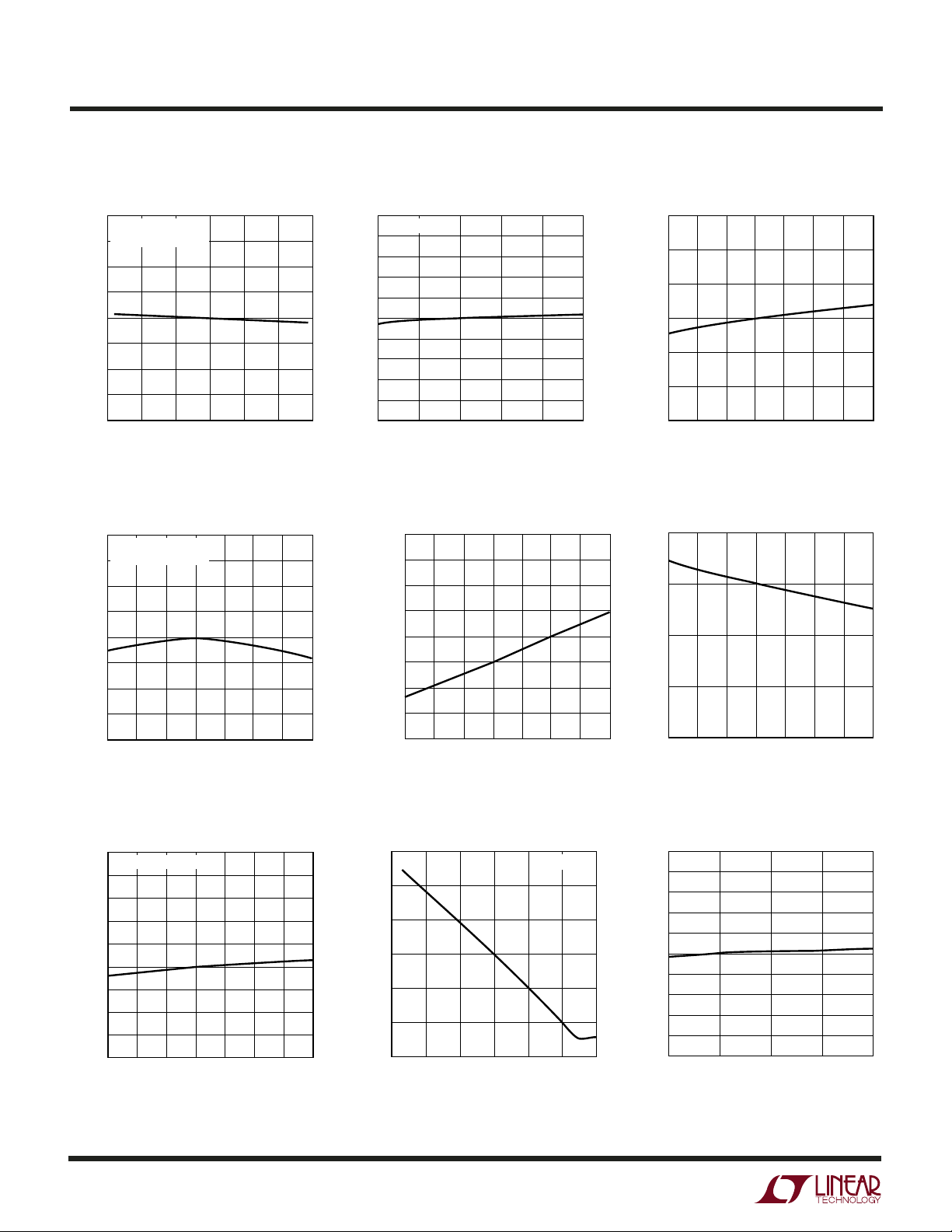
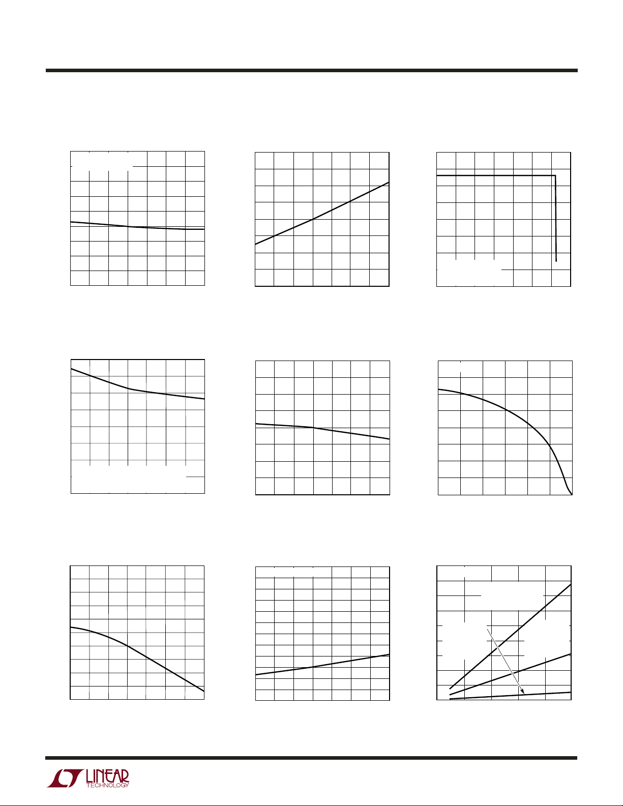
TYPICAL PERFOR A CE CHARACTERISTICS
Load Regulation
3.34
TA = 25°C
REFER TO FIGURE 12
3.33
3.32
3.31
(V)
3.30
OUT
V
3.29
3.28
3.27
3.26
–10 –5 5
–15
0
OUTPUT CURRENT (A)
10 15
3830 G02
Line Regulation
1.275
TA = 25°C
1.273
1.271
1.269
1.267
(V)
1.265
FB
V
1.263
1.261
1.259
1.257
1.255
3
4
5
SUPPLY VOLTAGE (V)
6
7
3830 G03
Error Amplifier Transconductance
vs Temperature
10
8
6
4
∆V
2
FB
(mV)
0
–2
–4
–6
–8
–10
8
Output Voltage Temperature Drift
3.34
REFER TO FIGURE 12
OUTPUT = NO LOAD
3.33
3.32
3.31
(V)
3.30
OUT
V
3.29
3.28
3.27
3.26
–25 0 50
–50
TEMPERATURE (°C)
Oscillator Frequency
vs Temperature
250
FREQSET FLOATING
240
230
220
210
200
190
180
OSCILLATOR FREQUENCY (kHz)
170
160
–50
–25
4
0
TEMPERATURE (°C)
25
25 125
75 100 125
50
75 100
3830 G04
3831 G08
∆V
OUT
(mV)
200
180
160
140
120
100
80
60
40
ERROR AMPLIFIER SINK/SOURCE CURRENT (µA)
–50
40
30
20
10
0
–10
–20
–30
–40
Oscillator Frequency
vs FREQSET Input Current
600
500
400
300
200
OSCILLATOR FREQUENCY (kHz)
100
0
–40
Error Amplifier Sink/Source
Current vs Temperature
–25 0 50
–30
FREQSET INPUT CURRENT (µA)
25
TEMPERATURE (°C)
–20 –10 0
75 100 125
TA = 25°C
10 20
3830 G09
3830 G06
Error Amplifier Open-Loop Gain
vs Temperature
Oscillator (V
SAWH
– V
SAWL
)
vs External Sync Frequency
3830fa
UW
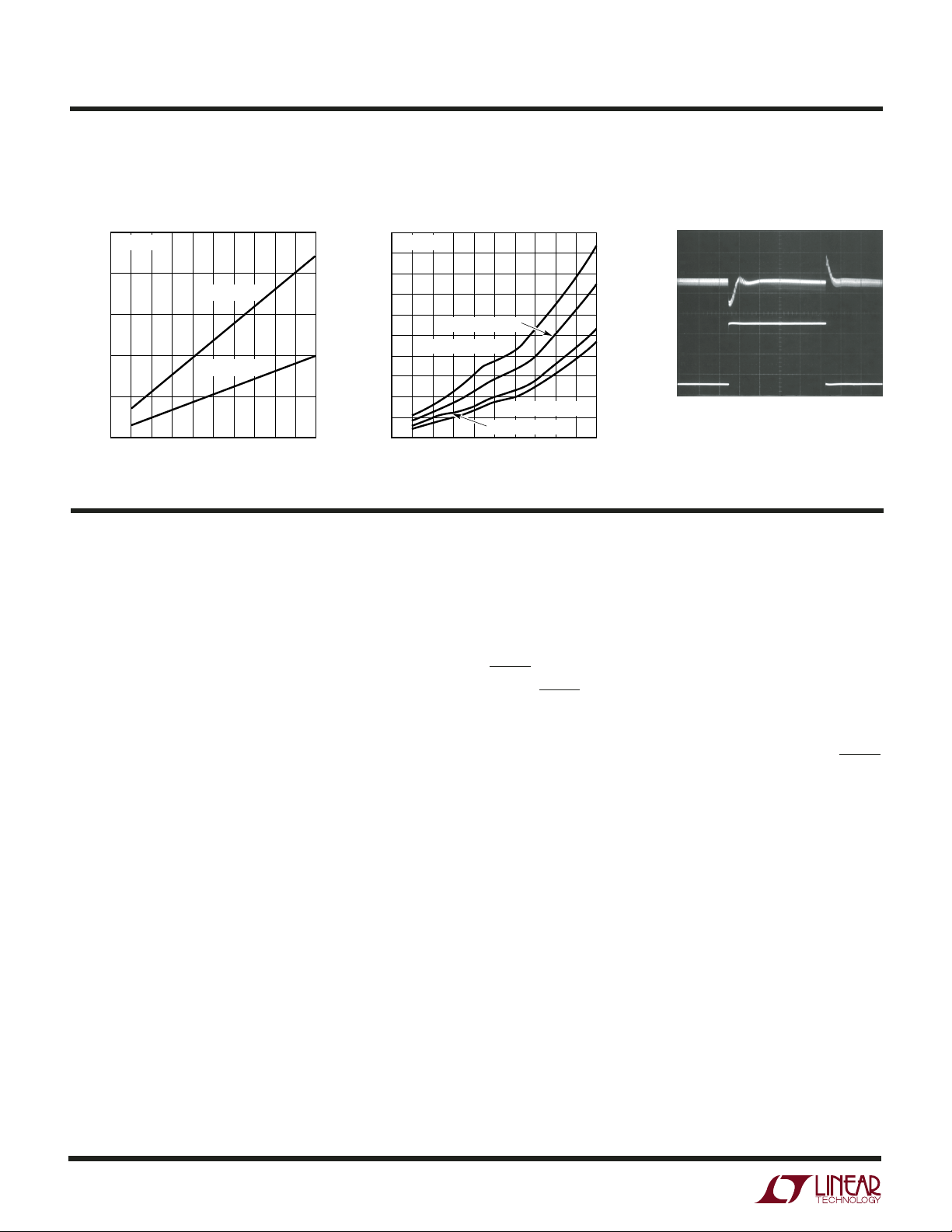
OUTPUT CURRENT (A)
0
4.0
3.5
3.0
2.5
2.0
1.5
1.0
0.5
0
3830 G13
2 4 6 8 10 12 14
OUTPUT VOLTAGE (V)
TA = 25°C
REFER TO FIGURE 12
R
IMAX
= 5k
TYPICAL PERFOR A CE CHARACTERISTICS
LTC3830/LTC3830-1
Maximum G1 Duty Cycle
vs Temperature
100
VFB = 0V
REFER TO FIGURE 3
99
98
97
96
95
94
93
MAXIMUM G1 DUTY CYCLE (%)
92
91
–50
0
–25
TEMPERATURE (°C)
25 125
50
Output Current Limit Threshold
vs Temperature
16
14
12
10
8
6
4
OUTPUT CURRENT LIMIT (A)
REFER TO FIGURE 12 AND NOTE 10 OF
2
THE ELECTRICAL CHARACTERISTICS
= 5k
R
IMAX
0
–50
0
–25
TEMPERATURE (°C)
50
25
75 100
75
100
3830 G11
3830 G14
125
I
Sink Current
MAX
vs Temperature Output Overcurrent Protection
20
18
16
14
12
10
SINK CURRENT (µA)
MAX
8
I
6
4
–25 0 50
–50
25
TEMPERATURE (°C)
Soft-Start Source Current
vs Temperature
–8
–9
–10
–11
–12
–13
–14
–15
SOFT-START SOURCE CURRENT (µA)
–16
–25 0 50
–50
25
TEMPERATURE (°C)
75 100 125
3830 G12
75 100 125
3830 G15
Soft-Start Sink Current
vs (V
– V
IFB
2.00
TA = 25°C
1.75
1.50
1.25
1.00
0.75
0.50
SOFT-START SINK CURRENT (mA)
0.25
0
–125 –100 –50
–150
IMAX
V
IFB
– V
)
–75
IMAX
(mV)
–25
0
3830 G16
3.0
2.9
2.8
2.7
2.6
2.5
2.4
2.3
2.2
2.1
2.0
–50
UNDERVOLTAGE LOCKOUT THRESHOLD VOLTAGE (V)
Undervoltage Lockout Threshold
Voltage vs Temperature
50
25
0
–25
TEMPERATURE (°C)
75
100
3830 G17
125
VCC Operating Supply Current
vs Temperature
1.6
FREQSET FLOATING
1.5
1.4
1.3
1.2
1.1
1.0
0.9
0.8
0.7
0.6
OPERATING SUPPLY CURRENT (mA)
CC
0.5
V
0.4
–50
0
–25
TEMPERATURE (°C)
50
25
PVCC Supply Current
vs Oscillator Frequency
90
TA = 25°C
80
70
60
50
G1 AND G2
40
WITH 1000pF,
PV
30
SUPPLY CURRENT (mA)
CC
20
PV
10
100
125
3830 G18
75
0
0
G1 AND G2 LOADED
WITH 6800pF,
= 12V
PV
CC1,2
G1 AND G2
LOADED
= 5V
CC1,2
100 300
200
OSCILLATOR FREQUENCY (kHz)
LOADED
WITH 6800pF,
PV
CC1,2
400
= 5V
500
3830 G19
3830fa
5
LTC3830/LTC3830-1
UW
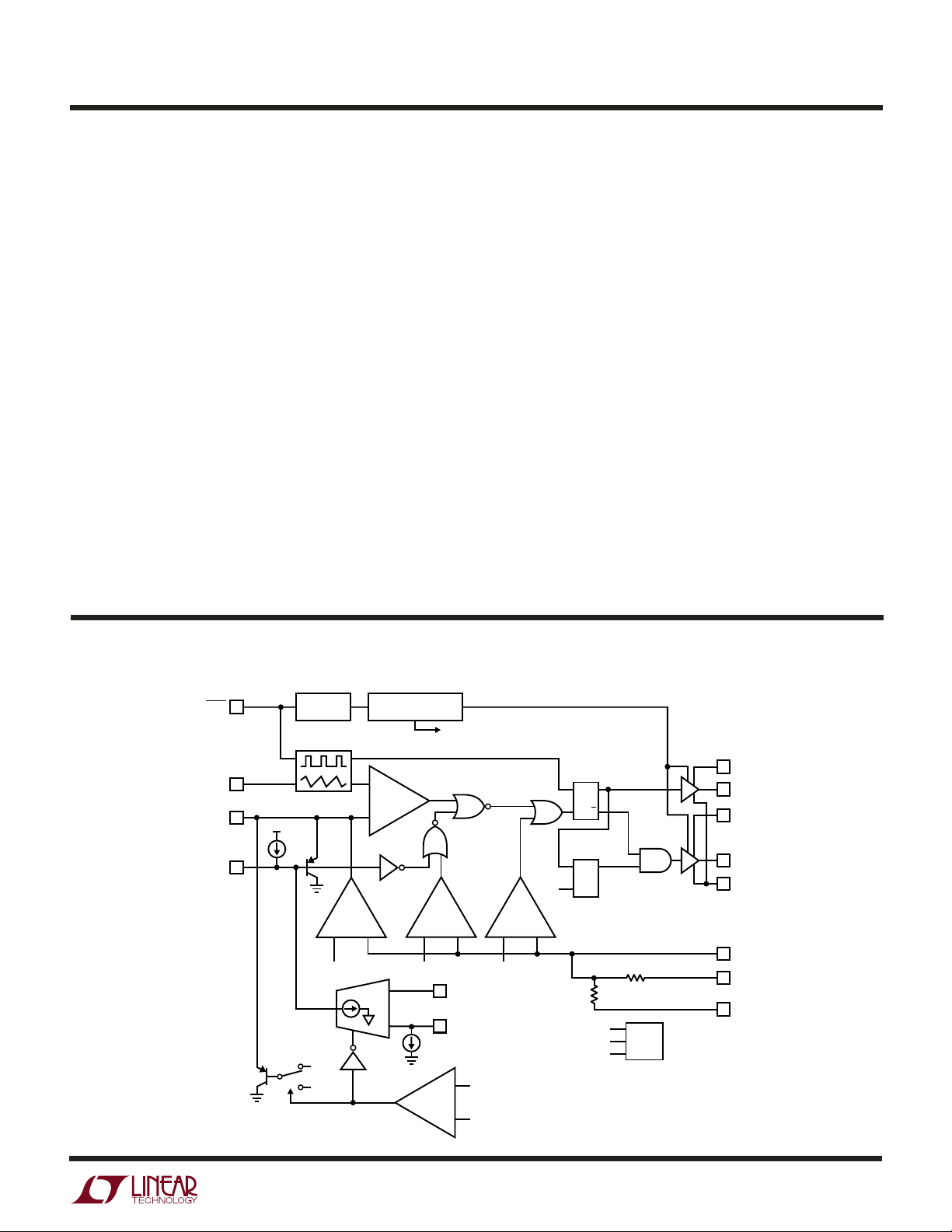
TYPICAL PERFOR A CE CHARACTERISTICS
PVCC Supply Current
vs Gate Capacitance
50
TA = 25°C
40
PV
CC1,2
30
20
SUPPLY CURRENT (mA)
CC
10
PV
0
123
0
GATE CAPACITANCE AT G1 AND G2 (nF)
PV
45
CC1,2
U
PI FU CTIO S
= 12V
= 5V
67 9
8
10
3830 G20
UU
(16-Lead LTC3830/8-Lead LTC3830/LTC3830-1)
G1 Rise/Fall Time
vs Gate Capacitance Transient Response
200
TA = 25°C
180
160
140
120
100
80
60
G1 RISE/FALL TIME (ns)
40
20
0
0
tf AT PV
t
AT PV
r
CC1,2
21
GATE CAPACITANCE AT G1 AND G2 (nF)
G1 (Pin 1/Pin 1/Pin 1): Top Gate Driver Output. Connect
this pin to the gate of the upper N-channel MOSFET, Q1.
This output swings from PGND to PV
. It remains low if
CC1
G2 is high or during shutdown mode.
V
OUT
50mV/DIV
= 5V
CC1,2
= 5V
AT PV
t
r
43
5
tf AT PV
67 9
CC1,2
CC1,2
= 12V
= 12V
8
10
3830 G21
I
LOAD
2AV/DIV
50µs/DIV
3830 G22.tif
resistor divider to set the output voltage, float SENSE+ and
SENSE– and connect the external resistor divider to FB.
The internal resistor divider is not included in the LTC3830-1
and the 8-lead LTC3830.
PV
(Pin 2/Pin 2/Pin 2): Power Supply Input for G1.
CC1
Connect this pin to a potential of at least VIN + V
GS(ON)(Q1)
.
This potential can be generated using an external supply or
charge pump.
PGND (Pin 3/Pin 3/Pin 3): Power Ground. Both drivers
return to this pin. Connect this pin to a low impedance
ground in close proximity to the source of Q2. Refer to the
Layout Consideration section for more details on PCB
layout techniques. The LTC3830-1 and the 8-lead LTC3830
have PGND and GND tied together internally at Pin 3.
GND (Pin 4/Pin 3/Pin 3): Signal Ground. All low power
internal circuitry returns to this pin. To minimize regulation errors due to ground currents, connect GND to PGND
right at the LTC3830.
SENSE–, FB, SENSE+ (Pins 5, 6, 7/Pin 4/Pin 4): These
three pins connect to the internal resistor divider and input
of the error amplifier. To use the internal divider to set the
output voltage to 3.3V, connect SENSE+ to the positive
terminal of the output capacitor and SENSE– to the negative terminal. FB should be left floating. To use an external
SHDN (Pin 8/Pin 5/NA): Shutdown. A TTL compatible low
level at SHDN for longer than 100µs puts the LTC3830 into
shutdown mode. In shutdown, G1 and G2 go low, all
internal circuits are disabled and the quiescent current
drops to 10µA max. A TTL compatible high level at SHDN
allows the part to operate normally. This pin also doubles
as an external clock input to synchronize the internal
oscillator with an external clock. The shutdown function is
disabled in the LTC3830-1.
SS (Pin 9/NA/Pin 5): Soft-Start. Connect this pin to an
external capacitor, CSS, to implement a soft-start function.
If the LTC3830 goes into current limit, CSS is discharged
to reduce the duty cycle. CSS must be selected such that
during power-up, the current through Q1 will not exceed
the current limit level. The soft-start function is disabled in
the 8-lead LTC3830.
COMP (Pin 10/Pin 6/Pin 6): External Compensation. This
pin internally connects to the output of the error amplifier
and input of the PWM comparator. Use a RC + C network
at this pin to compensate the feedback loop to provide
optimum transient response.
3830fa
6
LTC3830/LTC3830-1
U
UU
PI FU CTIO S
FREQSET (Pin 11/NA/NA): Frequency Set. Use this pin to
adjust the free-running frequency of the internal oscillator.
With the pin floating, the oscillator runs at about 200kHz.
A resistor from FREQSET to ground speeds up the oscillator; a resistor to V
(Pin 12/NA/NA): Current Limit Threshold Set. I
I
MAX
sets the threshold for the internal current limit comparator. If I
drops below I
FB
into current limit. I
GND. Connect this pin to the main V
of Q1, through an external resistor to set the current limit
threshold. Connect a 0.1µF decoupling capacitor across
this resistor to filter switching noise.
IFB (Pin 13/NA/NA): Current Limit Sense. Connect this pin
to the switching node at the source of Q1 and the drain of
Q2 through a 1k resistor. The 1k resistor is required to
prevent voltage transients from damaging IFB.This pin is
used for sensing the voltage drop across the upper
N-channel MOSFET, Q1.
slows it down.
CC
with G1 on, the LTC3830 goes
MAX
has an internal 12µA pull-down to
MAX
supply at the drain
IN
MAX
(Pin 14/Pin 7/Pin 7): Power Supply Input. All low
V
CC
power internal circuits draw their supply from this pin.
Connect this pin to a clean power supply, separate from
the main VIN supply at the drain of Q1. This pin requires a
4.7µF bypass capacitor. The LTC3830-1 and the 8-lead
LTC3830 have V
and PV
CC
tied together at Pin 7 and
CC2
require a 10µF bypass capacitor to GND.
PV
(Pin 15/Pin 7/Pin 7): Power Supply Input for G2.
CC2
Connect this pin to the main high power supply.
G2 (Pin 16/Pin 8/Pin 8): Bottom Gate Driver Output.
Connect this pin to the gate of the lower N-channel
MOSFET, Q2. This output swings from PGND to PV
CC2
. It
remains low when G1 is high or during shutdown mode.
To prevent output undershoot during a soft-start cycle, G2
is held low until G1 first goes high. (FFBG in Block
Diagram.)
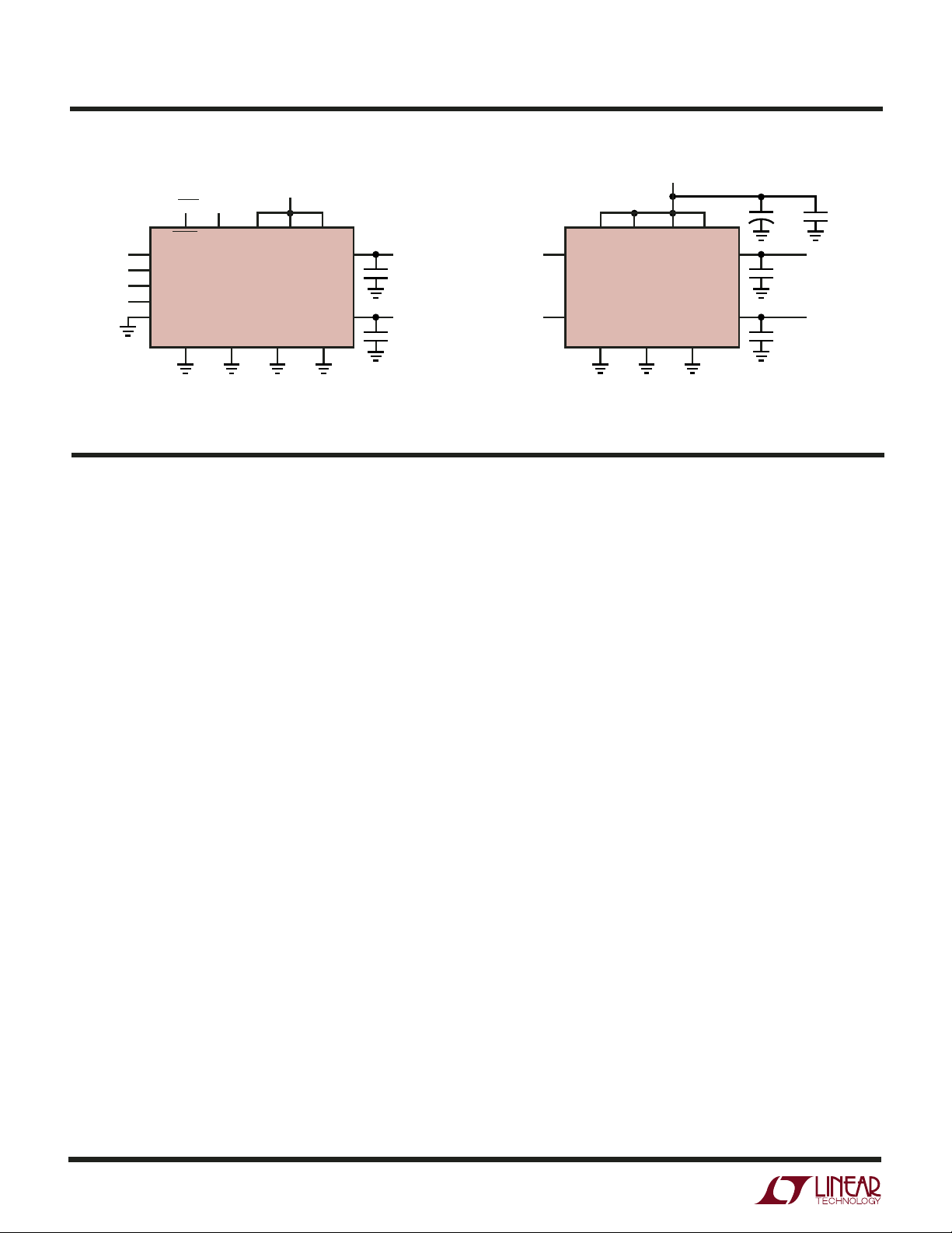
BLOCK DIAGRA
SHDN
FREQSET
COMP
SS
QC
W
12µA
100ms DELAY
INTERNAL
OSCILLATOR
QSS
+
V
REF
2.2V
1.2V
LOGIC AND
THERMAL SHUTDOWN
–
PWM
+
–
V
–
CC
+
DISABLE
ILIM
POWER DOWN
–
– 3% V
REF
I
FB
I
MAX
12µA
+
V
–
DISDR
PV
CC1
3830 BD
G1
PV
CC2
G2
PGND
FB
SENSE
SENSE
+
–
3830fa
Q
S
Q
R
FFBG
SQ
ENABLE
G2
RPOR
MAXMINERR
–
+ 3%
+
18k
11.2k
V
REF
V
– 3%
REF
+ 3%
V
REF
BG
+
REF
PV
CC1
+ 2.5V
V
CC1
7
LTC3830/LTC3830-1
COMP
FB
V
COMP
V
FB
G1
G2
I
FBVCCPVCC1
5V
PV
CC2
6800pF
0.1µF
10µF
6800pF
G1 RISE/FALL
G2 RISE/FALL
3830 F03
I
MAX
GND PGND
LTC3830
+
TEST CIRCUITS
PV
V
SHDNVCC
CC
NC
NC
NC
NC
SHDN V
FB
SS
FREQSET
COMP
I
MAX
CC
LTC3830
GND PGND SENSE
PV
CC2PVCC1
–
I
FB
SENSE
G1
G2
+
3830 F02
6800pF
6800pF
Figure 2 Figure 3
WUUU
APPLICATIO S I FOR ATIO
OVERVIEW
The LTC3830 is a voltage mode feedback, synchronous
switching regulator controller (see Block Diagram) designed for use in high power, low voltage step-down
(buck) converters. It includes an onboard PWM generator,
a precision reference trimmed to ±0.8%, two high power
MOSFET gate drivers and all necessary feedback and
control circuitry to form a complete switching regulator
circuit. The PWM loop nominally runs at 200kHz.
The 16-lead versions of the LTC3830 include a current
limit sensing circuit that uses the topside external N-channel
power MOSFET as a current sensing element, eliminating
the need for an external sense resistor.
Also included in the 16-lead version and the LTC3830-1
is an internal soft-start feature that requires only a single
external capacitor to operate. In addition, 16-lead parts
feature an adjustable oscillator that can free run or
synchronize to external signal with frequencies from
100kHz to 500kHz, allowing added flexibility in external
component selection. The 8-lead version does not include current limit, internal soft-start and frequency
adjustability. The LTC3830-1 does not include current
limit, frequency adjustability, external synchronization
and the shutdown function.
THEORY OF OPERATION
Primary Feedback Loop
The LTC3830/LTC3830-1 sense the output voltage of the
circuit at the output capacitor and feeds this voltage back
to the internal transconductance error amplifier, ERR,
through a resistor divider network. The error amplifier
compares the resistor-divided output voltage to the internal 1.265V reference and outputs an error signal to the
PWM comparator. This error signal is compared with a
fixed frequency ramp waveform, from the internal oscillator, to generate a pulse width modulated signal. This
PWM signal drives the external MOSFETs through the G1
and G2 pins. The resulting chopped waveform is filtered by
LO and C
which closes the loop. Loop compensation is
OUT
achieved with an external compensation network at the
COMP pin, the output node of the error amplifier.
MIN, MAX Feedback Loops
Two additional comparators in the feedback loop provide
high speed output voltage correction in situations where
the error amplifier may not respond quickly enough. MIN
compares the feedback signal to a voltage 40mV below the
internal reference. If the signal is below the comparator
threshold, the MIN comparator overrides the error amplifier and forces the loop to maximum duty cycle, >91%.
3830fa
8

WUUU
=
()()
()
()( )
VV V
fLV
IN OUT OUT
OSC O IN
–
APPLICATIO S I FOR ATIO
LTC3830/LTC3830-1
Similarly, the MAX comparator forces the output to 0%
duty cycle if the feedback signal is greater than 40mV
above the internal reference. To prevent these two comparators from triggering due to noise, the MIN and MAX
comparators’ response times are deliberately delayed by
two to three microseconds. These two comparators help
prevent extreme output perturbations with fast output
load current transients, while allowing the main feedback
loop to be optimally compensated for stability.
Thermal Shutdown
The LTC3830/LTC3830-1 have a thermal protection circuit that disables both gate drivers if activated. If the chip
junction temperature reaches 150°C, both G1 and G2 are
pulled low. G1 and G2 remain low until the junction
temperature drops below 125°C, after which, the chip
resumes normal operation.
Soft-Start and Current Limit
The 16-lead LTC3830 devices include a soft-start circuit
that is used for start-up and current limit operation. The
LTC3830-1 only has the soft-start function; the current
limit function is disabled. The 8-lead LTC3830 has both the
soft-start and current limit function disabled. The SS pin
requires an external capacitor, C
, to GND with the value
SS
determined by the required soft-start time. An internal
12µA current source is included to charge CSS. During
power-up, the COMP pin is clamped to a diode drop (B-E
junction of QSS in the Block Diagram) above the voltage at
the SS pin. This prevents the error amplifier from forcing
the loop to maximum duty cycle. The LTC3830/LTC3830-1
operate at low duty cycle as the SS pin rises above 0.6V
(V
≈ 1.2V). As SS continues to rise, QSS turns off and
COMP
the error amplifier takes over to regulate the output. The
MIN comparator is disabled during soft-start to prevent it
from overriding the soft-start function.
The 16-lead LTC3830 devices include yet another feedback loop to control operation in current limit. Just before
every falling edge of G1, the current comparator, CC,
samples and holds the voltage drop measured across the
external upper MOSFET, Q1, at the IFB pin. CC compares
the voltage at I
to the voltage at the I
FB
pin. As the peak
MAX
current rises, the measured voltage across Q1 increases
due to the drop across the R
drops below I
at I
FB
, indicating that Q1’s drain current
MAX
of Q1. When the voltage
DS(ON)
has exceeded the maximum level, CC starts to pull current
out of C
, cutting the duty cycle and controlling the output
SS
current level. The CC comparator pulls current out of the
SS pin in proportion to the voltage difference between I
and I
. Under minor overload conditions, the SS pin
MAX
FB
falls gradually, creating a time delay before current limit
takes effect. Very short, mild overloads may not affect the
output voltage at all. More significant overload conditions
allow the SS pin to reach a steady state, and the output
remains at a reduced voltage until the overload is removed. Serious overloads generate a large overdrive at
CC, allowing it to pull SS down quickly and preventing
damage to the output components. By using the R
DS(ON)
of Q1 to measure the output current, the current limiting
circuit eliminates an expensive discrete sense resistor that
would otherwise be required. This helps minimize the
number of components in the high current path.
The current limit threshold can be set by connecting an
external resistor R
supply at the drain of Q1. The value of R
IMAX
from the I
pin to the main V
MAX
is determined
IMAX
IN
by:
R
IMAX
= (I
LMAX
)(R
DS(ON)Q1
)/I
IMAX
where:
I
= I
LMAX
I
= Maximum load current
LOAD
I
RIPPLE
LOAD
+ (I
RIPPLE
/2)
= Inductor ripple current
f
= LTC3830 oscillator frequency = 200kHz
OSC
LO = Inductor value
R
DS(ON)Q1
I
IMAX
= On-resistance of Q1 at I
LMAX
= Internal 12µA sink current at I
MAX
3830fa
9

LTC3830/LTC3830-1
WUUU
APPLICATIO S I FOR ATIO
The R
of Q1 usually increases with temperature. To
DS(ON)
keep the current limit threshold constant, the internal
12µA sink current at I
is designed with a positive
MAX
temperature coefficient to provide first order correction
for the temperature coefficient of R
DS(ON)Q1
.
In order for the current limit circuit to operate properly and
to obtain a reasonably accurate current limit threshold, the
I
IMAX
and I
pins must be Kelvin sensed at Q1’s drain and
FB
source pins. In addition, connect a 0.1µF decoupling
capacitor across R
to filter switching noise. Other-
IMAX
wise, noise spikes or ringing at Q1’s source can cause the
actual current limit to be greater than the desired current
limit set point. Due to switching noise and variation of
R
, the actual current limit trip point is not highly
DS(ON)
accurate. The current limiting circuitry is primarily meant
to prevent damage to the power supply circuitry during
fault conditions. The exact current level where the limiting
circuit begins to take effect will vary from unit to unit as the
R
±40% and with ±25% variation on the LTC3830’s I
of Q1 varies. Typically, R
DS(ON)
varies as much as
DS(ON)
MAX
current, this can give a ±65% variation on the current limit
threshold.
The R
low. This occurs during power up, when PV
up. To prevent the high R
is high if the VGS applied to the MOSFET is
DS(ON)
CC1
from activating the current
DS(ON)
is ramping
limit, the LTC3830 disables the current limit circuit if
PV
is less than 2.5V above VCC. To ensure proper
CC1
V
IN
LTC3830
R
IMAX
+
CC
–
12µA
I
12
MAX
I
FB
13
0.1µF
G1
1k
G2
Q1
Q2
+
C
IN
L
O
V
OUT
+
C
OUT
3830 F04
operation of the current limit circuit, PV
least 2.5V above V
when G1 is high. PV
CC
must be at
CC1
can go low
CC1
when G1 is low, allowing the use of an external charge
pump to power PV
CC1
.
Oscillator Frequency
The LTC3830 includes an onboard current controlled
oscillator that typically free-runs at 200kHz. The oscillator
frequency can be adjusted by forcing current into or out of
the FREQSET pin. With the pin floating, the oscillator runs
at about 200kHz. Every additional 1µA of current into/out
of the FREQSET pin decreases/increases the frequency by
10kHz. The pin is internally servoed to 1.265V, connecting
a 50k resistor from FREQSET to ground forces 25µA out
of the pin, causing the internal oscillator to run at approximately 450kHz. Forcing an external 10µA current into
FREQSET cuts the internal frequency to 100kHz. An internal clamp prevents the oscillator from running slower than
about 50kHz. Tying FREQSET to V
forces the chip to run
CC
at this minimum speed. The LTC3830-1 and the 8-lead
LTC3830 do not have this frequency adjustment function.
Shutdown
The LTC3830 includes a low power shutdown mode,
controlled by the logic at the SHDN pin. A high at SHDN
allows the part to operate normally. A low level at SHDN for
more than 100µs forces the LTC3830 into shutdown
mode. In this mode, all internal switching stops, the COMP
and SS pins pull to ground and Q1 and Q2 turn off. The
LTC3830 supply current drops to <10µA, although off-
state leakage in the external MOSFETs may cause the total
VIN current to be some what higher, especially at elevated
temperatures. If SHDN returns high, the LTC3830 reruns
a soft-start cycle and resumes normal operation. The
LTC3830-1 does not have this shutdown function.
10
Figure 4. Current Limit Setting
3830fa

WUUU
APPLICATIO S I FOR ATIO
LTC3830/LTC3830-1
External Clock Synchronization
The LTC3830 SHDN pin doubles as an external clock input
for applications that require a synchronized clock. An
internal circuit forces the LTC3830 into external synchronization mode if a negative transition at the SHDN pin is
detected. In this mode, every negative transition on the
SHDN pin resets the internal oscillator and pulls the ramp
signal low, this forces the LTC3830 internal oscillator to
lock to the external clock frequency. The LTC3830-1 does
not have this external synchronization function.
The LTC3830 internal oscillator can be externally synchronized from 100kHz to 500kHz. Frequencies above 300kHz
can cause a decrease in the maximum obtainable duty
cycle as rise/fall time and propagation delay take up a
larger percentage of the switch cycle. Circuits using these
frequencies should be checked carefully in applications
where operation near dropout is important—like 3.3V to
SHDN
2.5V converters. The low period of this clock signal must
not be >100µs, or else the LTC3830 enters shutdown
mode.
Figure 5 describes the operation of the external synchronization function. A negative transition at the SHDN pin
forces the internal ramp signal low to restart a new PWM
cycle. Notice that with the traditional sync method, the
ramp amplitude is lowered as the external clock frequency
goes higher. The effect of this decrease in ramp amplitude
increases the open-loop gain of the controller feedback
loop. As a result, the loop crossover frequency increases
and it may cause the feedback loop to be unstable if the
phase margin is insufficient.
To overcome this problem, the LTC3830 monitors the
peak voltage of the ramp signal and adjusts the oscillator
charging current to maintain a constant ramp peak.
V
CC
INTERNAL
CIRCUITRY
PV
CC2
PV
CC1
V
IN
G1
Q1
L
O
G2
Q2
V
OUT
+
C
OUT
TRADITIONAL
SYNC METHOD
WITH EARLY
RAMP
TERMINATION
RAMP AMPLITUDE
LTC3830
KEEPS RAMP
AMPLITUDE
CONSTANT
UNDER SYNC
200kHz
FREE RUNNING
RAMP SIGNAL
ADJUSTED
RAMP SIGNAL
WITH EXT SYNC
Figure 5. External Synchronization Operation
3830 F05
LTC3830 (16-LEAD)
VCC/PV
CC2
INTERNAL
CIRCUITRY
LTC3830 (8-LEAD)
Figure 6. 16-Lead Power Supplies
PV
CC1
V
IN
G1
Q1
L
O
G2
Q2
Figure 7. 8-Lead Power Supplies
3830 F6
V
OUT
+
C
OUT
3830 F7
3830fa
11

LTC3830/LTC3830-1
WUUU
APPLICATIO S I FOR ATIO
Input Supply Considerations/Charge Pump
The 16-lead LTC3830 requires four supply voltages to
operate: V
MOSFET gate drive and a clean, low ripple V
for the main power input, PV
IN
CC1
and PV
CC
for
CC2
for the
LTC3830 internal circuitry (Figure 6). The LTC3830-1 and
the 8-lead LTC3830 have the PV
and VCC pins tied
CC2
together inside the package (Figure 7). This pin, brought
out as VCC/PV
, has the same low ripple requirements
CC2
as the 16-lead part, but must also be able to supply the gate
drive current to Q2.
In many applications, V
can be powered from V
CC
IN
through an RC filter. This supply can be as low as 3V. The
low quiescent current (typically 800µA) allows the use of
relatively large filter resistors and correspondingly small
filter capacitors. 100Ω and 4.7µF usually provide ad-
equate filtering for VCC. For best performance, connect the
4.7µF bypass capacitor as close to the LTC3830 VCC pin as
possible.
Gate drive for the top N-channel MOSFET Q1 is supplied
from PV
power supply input) by at least one power MOSFET V
for efficient operation. An internal level shifter allows PV
to operate at voltages above V
. This supply must be above VIN (the main
CC1
and VIN, up to 14V maxi-
CC
GS(ON)
CC1
mum. This higher voltage can be supplied with a separate
supply, or it can be generated using a charge pump.
Gate drive for the bottom MOSFET Q2 is provided through
PV
for the 16-lead LTC3830 or VCC/PV
CC2
CC2
for the
LTC3830-1 and the 8-lead LTC3830. This supply only
needs to be above the power MOSFET V
operation. PV
charge pump for the PV
can also be driven from the same supply/
CC2
, or it can be connected to a
CC1
GS(ON)
for efficient
lower supply to improve efficiency.
Figure 8 shows a tripling charge pump circuit that can be
used to provide 2VIN and 3VIN gate drive for the external
top and bottom MOSFETs respectively. These should fully
enhance MOSFETs with 5V logic level thresholds. This
circuit provides 3VIN – 3VF to PV
– 2VF to PV
2V
IN
where VF is the forward voltage of the
CC2
while Q1 is ON and
CC1
Schottky diodes. The circuit requires the use of Schottky
diodes to minimize forward drop across the diodes at
start-up. The tripling charge pump circuit can rectify any
ringing at the drain of Q2 and provide more than 3V
PV
; a 12V zener diode should be included from PV
CC1
IN
at
CC1
to PGND to prevent transients from damaging the circuitry
at PV
or the gate of Q1.
CC1
The charge pump capacitors refresh when the G2 pin goes
high and the switch node is pulled low by Q2. The G2 ontime becomes narrow when LTC3830 operates at maximum duty cycle (95% typical), which can occur if the input
supply rises more slowly than the soft-start capacitor or
the input voltage droops during load transients. If the G2
on-time gets so narrow that the switch node fails to pull
completely to ground, the charge pump voltage may
collapse or fail to start, causing excessive dissipation in
external MOSFET Q1. This is most likely with low V
CC
voltages and high switching frequencies, coupled with
large external MOSFETs which slow the G2 and switch
node slew rates.
12
D
Z
12V
1N5242
10µF
LTC3830
1N5817
1N5817
PV
PV
CC2
CC1
G1
G2
Figure 8. Tripling Charge Pump
1N5817
0.1µF
0.1µF
V
IN
Q1
L
O
Q2 C
V
OUT
+
OUT
3830 F08
3830fa

WUUU
APPLICATIO S I FOR ATIO
LTC3830/LTC3830-1
The LTC3830/LTC3830-1 overcomes this problem by
sensing the PV
voltage when G1 is high. If PV
CC1
CC1
is less
than (VCC + 2.5V), the maximum G1 duty cycle is reduced
to 70% by clamping the COMP pin at 1.8V (QC in BLOCK
DIAGRAM). This increases the G2 on time and allows the
charge pump capacitor to be refreshed.
For Applications using an external supply to power PV
this supply must also be higher than V
by at least 2.5V
CC
CC1
,
to insure normal operation.
For applications with a 5V or higher V
be tied to V
if a logic level MOSFET is used. PV
IN
IN
supply, PV
CC1
can
CC2
can be
supplied using a doubling charge pump as shown in Figure
9. This circuit provides 2VIN – VF to PV
while Q1 is ON.
CC1
Figure 12 shows a typical 5V to 3.3V application using a
doubling charge pump to generate PV
CC1
.
Power MOSFETs
Two N-channel power MOSFETs are required for most
LTC3830 circuits. These should be selected based
primarily on threshold voltage and on-resistance considerations. Thermal dissipation is often a secondary concern in high efficiency designs. The required MOSFET
threshold should be determined based on the available
power supply voltages and/or the complexity of the gate
drive charge pump scheme. In 3.3V input designs where
V
IN
OPTIONAL
USE FOR V
D
Z
12V
1N5242
≥ 7V
IN
CC2
PV
PV
LTC3830
Figure 9. Doubling Charge Pump
CC1
G1
G2
MBR0530T1
0.1µF
Q1
L
O
Q2 C
+
3830 F09
OUT
V
OUT
an auxiliary 12V supply is available to power PV
PV
, standard MOSFETs with R
CC2
DS(ON)
specified at V
CC1
and
GS
= 5V or 6V can be used with good results. The current
drawn from this supply varies with the MOSFETs used
and the LTC3830’s operating frequency, but is generally
less than 50mA.
LTC3830 applications that use 5V or lower VIN voltage and
a doubling/tripling charge pump to generate PV
PV
, do not provide enough gate drive voltage to fully
CC2
CC1
and
enhance standard power MOSFETs. Under this condition,
the effective MOSFET R
may be quite high, raising
DS(ON)
the dissipation in the FETs and reducing efficiency. Logic
level FETs are the recommended choice for 5V or lower
voltage systems. Logic level FETs can be fully enhanced
with a doubler/tripling charge pump and will operate at
maximum efficiency.
After the MOSFET threshold voltage is selected, choose the
R
based on the input voltage, the output voltage,
DS(ON)
allowable power dissipation and maximum output current.
In a typical LTC3830 circuit, operating in continuous mode,
the average inductor current is equal to the output load
current. This current flows through either Q1 or Q2 with the
power dissipation split up according to the duty cycle:
V
DC Q
DC Q
The R
()
() –
DS(ON)
OUT
1
=
V
IN
V
21
==
OUT
V
IN
VV
–
IN OUT
V
IN
required for a given conduction loss can now
be calculated by rearranging the relation P = I2R.
R
DS ON Q
R
DS ON Q
()
()
P
MAX Q
() ()
==
1
DC Q I
()•( )
P
==
2
DC Q I
()•( )•(– )•( )
1
1
LOAD
MAX Q
() ()
2
2
LOAD
VP
•
IN MAX Q
2
VI
•( )
OUT LOAD
VP
IN MAX Q
2
VV I
IN OUT LOAD
1
2
2
2
3830fa
13

LTC3830/LTC3830-1
WUUU
APPLICATIO S I FOR ATIO
P
should be calculated based primarily on required
MAX
efficiency or allowable thermal dissipation. A typical high
efficiency circuit designed for 5V input and 3.3V at 10A
output might allow no more than 3% efficiency loss at full
load for each MOSFET. Assuming roughly 90% efficiency
at this current level, this gives a P
(3.3V)(10A/0.9)(0.03) = 1.1W per FET
and a required R
()•(.)
R
DS ON Q
()
R
DS ON Q
()
==Ω
1
( . )( )
==Ω
2
(–.)( )
Note that the required R
of:
DS(ON)
511
VW
33 10
VA
()•(.)
511
VW
53310
VVA
2
for Q2 is roughly twice that
DS(ON)
of Q1 in this example. This application might specify a
single 0.03Ω device for Q2 and parallel two more of the
same devices to form Q1. Note also that while the required
R
values suggest large MOSFETs, the power dissi-
DS(ON)
pation numbers are only 1.1W per device or less; large
TO-220 packages and heat sinks are not necessarily
required in high efficiency applications. Siliconix Si4410DY
MAX
.
0 017
2
value of:
.
0 032
or International Rectifier IRF7413 (both in SO-8) or Siliconix
SUD50N03-10 (TO-252) or ON Semiconductor
MTD20N03HDL (DPAK) are small footprint surface mount
devices with R
work well in LTC3830 circuits. Using a higher P
in the R
calculations generally decreases the MOSFET
DS(ON)
values below 0.03Ω at 5V of VGS that
DS(ON)
MAX
value
cost and the circuit efficiency and increases the MOSFET
heat sink requirements.
Table 1 highlights a variety of power MOSFETs for use in
LTC3830 applications.
Inductor Selection
The inductor is often the largest component in an LTC3830
design and must be chosen carefully. Choose the inductor
value and type based on output slew rate requirements. The
maximum rate of rise of inductor current is set by the
inductor’s value, the input-to-output voltage differential and
the LTC3830’s maximum duty cycle. In a typical 5V input,
3.3V output application, the maximum rise time will be:
DC V V
•( – ) .
MAX IN OUT
LL
OO
=
1 615
A
s
µ
Table 1. Recommended MOSFETs for LTC3830 Applications
TYPICAL INPUT
R
PARTS AT 25°C (mΩ) RATED CURRENT (A) C
Siliconix SUD50N03-10 19 15 at 25°C 3200 1.8 175
TO-252 10 at 100°C
Siliconix Si4410DY 20 10 at 25°C 2700 150
SO-8 8 at 70°C
ON Semiconductor MTD20N03HDL 35 20 at 25°C 880 1.67 150
DPAK 16 at 100°C
Fairchild FDS6670A 8 13 at 25°C 3200 25 150
S0-8
Fairchild FDS6680 10 11.5 at 25°C 2070 25 150
SO-8
ON Semiconductor MTB75N03HDL 9 75 at 25°C 4025 1 150
DD PAK 59 at 100°C
IR IRL3103S 19 64 at 25°C 1600 1.4 175
DD PAK 45 at 100°C
IR IRLZ44 28 50 at 25°C 3300 1 175
TO-220 36 at 100°C
Fuji 2SK1388 37 35 at 25°C 1750 2.08 150
TO-220
Note: Please refer to the manufacturer’s data sheet for testing conditions and detailed information.
DS(ON)
CAPACITANCE
(pF) θJC (°C/W) T
ISS
JMAX
(°C)
3830fa
14

WUUU
APPLICATIO S I FOR ATIO
LTC3830/LTC3830-1
where LO is the inductor value in µH. With proper fre-
quency compensation, the combination of the inductor
and output capacitor values determine the transient recovery time. In general, a smaller value inductor improves
transient response at the expense of ripple and inductor
core saturation rating. A 2µH inductor has a 0.81A/µs rise
time in this application, resulting in a 6.2µs delay in
responding to a 5A load current step. During this 6.2µs,
the difference between the inductor current and the output
current is made up by the output capacitor. This action
causes a temporary voltage droop at the output. To
minimize this effect, the inductor value should usually be
in the 1µH to 5µH range for most 5V input LTC3830
circuits. To optimize performance, different combinations
of input and output voltages and expected loads may
require different inductor values.
Once the required value is known, the inductor core type
can be chosen based on peak current and efficiency
requirements. Peak current in the inductor will be equal to
the maximum output load current plus half of the peak-topeak inductor ripple current. Ripple current is set by the
inductor value, the input and output voltage and the
operating frequency. The ripple current is approximately
equal to:
VV V
−()•()
I
RIPPLE
f
= LTC3830 oscillator frequency = 200kHz
OSC
LO = Inductor value
Solving this equation with our typical 5V to 3.3V application with a 2µH inductor, we get:
(–.)•.
53333
VVV
200 2 5
kHz H V
IN OUT OUT
=
fLV
••
OSC O IN
••
µ
=
.
28
A
P
-P
Peak inductor current at 10A load:
10A + (2.8A/2) = 11.4A
The ripple current should generally be between 10% and
40% of the output current. The inductor must be able to
withstand this peak current without saturating, and the
copper resistance in the winding should be kept as low as
possible to minimize resistive power loss. Note that in
circuits not employing the current limit function, the
current in the inductor may rise above this maximum
under short-circuit or fault conditions; the inductor should
be sized accordingly to withstand this additional current.
Inductors with gradual saturation characteristics are often
the best choice.
Input and Output Capacitors
A typical LTC3830 design places significant demands on
both the input and the output capacitors. During normal
steady load operation, a buck converter like the LTC3830
draws square waves of current from the input supply at the
switching frequency. The peak current value is equal to the
output load current plus 1/2 the peak-to-peak ripple current. Most of this current is supplied by the input bypass
capacitor. The resulting RMS current flow in the input
capacitor heats it and causes premature capacitor failure
in extreme cases. Maximum RMS current occurs with
50% PWM duty cycle, giving an RMS current value equal
to I
ripple current rating must be used to ensure reliable
operation. Note that capacitor manufacturers’ ripple current ratings are often based on only 2000 hours (3 months)
lifetime at rated temperature. Further derating of the input
capacitor ripple current beyond the manufacturer’s specification is recommended to extend the useful life of the
circuit. Lower operating temperature has the largest effect
on capacitor longevity.
/2. A low ESR input capacitor with an adequate
OUT
3830fa
15

LTC3830/LTC3830-1
fLC
LC O OUT
= π
[]
12/ ( )( )
3830 F10a
LTC3830
V
REF
R1
SENSE
–
R2
C2
SENSE
+
–
+
5
V
FB
6
COMP
10
7
C1
C
C
R
C
ERR
WUUU
APPLICATIO S I FOR ATIO
The output capacitor in a buck converter under steadystate conditions sees much less ripple current than the
input capacitor. Peak-to-peak current is equal to inductor
ripple current, usually 10% to 40% of the total load
current. Output capacitor duty places a premium not on
power dissipation but on ESR. During an output load
transient, the output capacitor must supply all of the
additional load current demanded by the load until the
LTC3830 adjusts the inductor current to the new value.
ESR in the output capacitor results in a step in the output
voltage equal to the ESR value multiplied by the change in
load current. An 5A load step with a 0.05Ω ESR output
capacitor results in a 250mV output voltage shift; this is
7.6% of the output voltage for a 3.3V supply! Because of
the strong relationship between output capacitor ESR and
output load transient response, choose the output capacitor for ESR, not for capacitance value. A capacitor with
suitable ESR will usually have a larger capacitance value
than is needed to control steady-state output ripple.
Electrolytic capacitors rated for use in switching power
supplies with specified ripple current ratings and ESR can
be used effectively in LTC3830 applications. OS-CON
electrolytic capacitors from Sanyo and other manufacturers give excellent performance and have a very high
performance/size ratio for electrolytic capacitors. Surface
mount applications can use either electrolytic or dry
tantalum capacitors. Tantalum capacitors must be surge
tested and specified for use in switching power supplies.
Low cost, generic tantalums are known to have very short
lives followed by explosive deaths in switching power
supply applications. Other capacitors that can be used
include the Sanyo POSCAP and MV-WX series.
a maximum rated ESR of 0.04Ω; three in parallel lower
the net output capacitor ESR to 0.013Ω.
Feedback Loop Compensation
The LTC3830 voltage feedback loop is compensated at the
COMP pin, which is the output node of the error amplifier.
The feedback loop is generally compensated with an RC +
C network from COMP to GND as shown in Figure 10a.
Loop stability is affected by the values of the inductor, the
output capacitor, the output capacitor ESR, the error
amplifier transconductance and the error amplifier compensation network. The inductor and the output capacitor
create a double pole at the frequency:
The ESR of the output capacitor and the output capacitor
value form a zero at the frequency:
f ESR C
= π
12/ ( )( )
ESR OUT
[]
The compensation network used with the error amplifier
must provide enough phase margin at the 0dB crossover
frequency for the overall open-loop transfer function. The
zero and pole from the compensation network are:
fZ = 1/[2π(RC)(CC)] and
fP = 1/[2π(RC)(C1)] respectively
A common way to lower ESR and raise ripple current
capability is to parallel several capacitors. A typical
LTC3830 application might exhibit 5A input ripple current. Sanyo OS-CON capacitors, part number 10SA220M
(220µF/10V), feature 2.3A allowable ripple current at
85°C; three in parallel at the input (to withstand the input
ripple current) meet the above requirements. Similarly,
Sanyo POSCAP 4TPB470M (470µF/4V) capacitors have
16
Figure 10a. Compensation Pin Hook-Up
3830fa

WUUU
APPLICATIO S I FOR ATIO
LTC3830/LTC3830-1
Figure 10b shows the Bode plot of the overall transfer
function.
When low ESR output capacitors (Sanyo OS-CON) are
used, the ESR zero can be high enough in frequency that
it provides little phase boost at the loop crossover frequency. As a result, the phase margin becomes inadequate and the load transient is not optimized. To resolve
this problem, a small capacitor can be connected between
the top of the resistor divider network and the V
pin to
FB
create a pole-zero pair in the loop compensation. The zero
location is prior to the pole location and thus, phase lead
can be added to boost the phase margin at the loop
crossover frequency. The pole and zero locations are
located at:
f
= 1/[2π(R2)(C2)] and
ZC2
f
= 1/[2π(R1||R2)(C2)]
PC2
where R1||R2 is the parallel combination resistance of R1
and R2. Choose C2 so that the zero is located at a lower
frequency compared to fCO and the pole location is high
enough that the closed loop has enough phase margin for
stability. Figure 10c shows the Bode plot using phase
lead compensation around the LTC3830 resistor divider
network.
Note: This technique is effective only when
R1 >> R2 i.e., at high output voltages only so that the pole
and zero are sufficiently separated.
Although a mathematical approach to frequency compensation can be used, the added complication of input and/or
output filters, unknown capacitor ESR, and gross operating point changes with input voltage, load current variations, all suggest a more practical empirical method. This
can be done by injecting a transient current at the load and
using an RC network box to iterate toward the final values,
or by obtaining the optimum loop response using a
network analyzer to find the actual loop poles and zeros.
Table 2 shows the suggested compensation component
value for 5V to 3.3V applications based on Sanyo OS-CON
4SP820M low ESR output capacitors.
Table 2. Recommended Compensation Network for 5V to 3.3V
Applications Using Multiple Paralleled 820µF Sanyo OS-CON
4SP820M Output Capacitors
L1 (µH) C
1.2 1640 6.2 3.3 470 1000
1.2 2460 12 3.3 470 1000
1.2 4100 12 1.8 220 1000
2.4 1640 15 2.7 330 1000
2.4 2460 20 1.0 220 1000
2.4 4100 36 1.0 220 1000
4.7 1640 30 1.8 330 1000
4.7 2460 36 1.0 180 1000
4.7 4100 82 1.0 180 1000
(µF) RC (kΩ)CC (nF) C1 (pF) C2 (pF)
OUT
f
LOOP GAIN
= LTC3830 SWITCHING
SW
f
Z
f
f
LC
ESR
FREQUENCY
= CLOSED-LOOP CROSSOVER
f
CO
FREQUENCY
20dB/DECADE
f
P
f
CO
f
Z
LOOP GAIN
FREQUENCY FREQUENCY
3830 F10b
f
f
LC
= LTC3830 SWITCHING
f
SW
FREQUENCY
= CLOSED-LOOP CROSSOVER
f
CO
FREQUENCY
20dB/DECADE
f
CO
ZC2
f
ESR
fPf
PC2
3830 F10c
Figure 10b. Bode Plot of the LTC3830 Overall Transfer Function Figure 10c. Bode Plot of the LTC3830 Overall
Transfer Function Using a Low ESR Output Capacitor
3830fa
17

LTC3830/LTC3830-1
WUUU
APPLICATIO S I FOR ATIO
Table 3 shows the suggested compensation component
values for 5V to 3.3V applications based on 470µF Sanyo
POSCAP 4TPB470M output capacitors.
Table 3. Recommended Compensation Network for 5V to 3.3V
Applications Using Multiple Paralleled 470µF Sanyo POSCAP
4TPB470M Output Capacitors
L1 (µH) C
1.2 1410 6.8 4.7 33
1.2 2820 15 2.2 33
1.2 4700 22 2.2 33
2.4 1410 18 10 33
2.4 2820 43 2.2 33
2.4 4700 62 2.2 10
4.7 1410 43 10 10
4.7 2820 91 33 10
4.7 4700 150 10 10
(µF) RC (kΩ)C
OUT
(nF) C1 (pF)
C
Table 4 shows the suggested compensation component
values for 5V to 3.3V applications based on 1500µF Sanyo
MV-WX output capacitors.
Table 4. Recommended Compensation Network for 5V to 3.3V
Applications Using Multiple Paralleled 1500µF Sanyo MV-WX
Output Capacitors
L1 (µH) C
1.2 4500 22 1.5 120
1.2 6000 30 1 82
1.2 9000 39 0.47 56
2.4 4500 51 1 56
2.4 6000 62 1 33
2.4 9000 82 0.47 27
4.7 4500 100 3.3 15
4.7 6000 150 0.47 15
4.7 9000 200 0.47 15
(µF) RC (kΩ)C
OUT
(nF) C1 (pF)
C
LAYOUT CONSIDERATIONS
When laying out the printed circuit board, use the following checklist to ensure proper operation of the LTC3830.
These items are also illustrated graphically in the layout
diagram of Figure 11. The thicker lines show the high
current paths. Note that at 10A current levels or above,
current density in the PC board itself is a serious concern.
Traces carrying high current should be as wide as possible. For example, a PCB fabricated with 2oz copper
requires a minimum trace width of 0.15" to carry 10A.
1. In general, layout should begin with the location of the
power devices. Be sure to orient the power circuitry so that
a clean power flow path is achieved. Conductor widths
should be maximized and lengths minimized. After you are
satisfied with the power path, the control circuitry should
be laid out. It is much easier to find routes for the relatively
small traces in the control circuits than it is to find
circuitous routes for high current paths.
2. The GND and PGND pins should be shorted directly at
the LTC3830. This helps to minimize internal ground disturbances in the LTC3830 and prevent differences in ground
potential from disrupting internal circuit operation. This
connection should then tie into the ground plane at a single
point, preferably at a fairly quiet point in the circuit such as
close to the output capacitors. This is not always practical,
however, due to physical constraints. Another reasonably
good point to make this connection is between the output
capacitors and the source connection of the bottom
MOSFET Q2. Do not tie this single point ground in the trace
run between the Q2 source and the input capacitor ground,
as this area of the ground plane will be very noisy.
18
3830fa

WUUU
APPLICATIO S I FOR ATIO
LTC3830/LTC3830-1
3. The small-signal resistors and capacitors for frequency
compensation and soft-start should be located very close
to their respective pins and the ground ends connected to
the signal ground pin through a separate trace. Do not
connect these parts to the ground plane!
4. The V
CC
, PV
CC1
and PV
decoupling capacitors should
CC2
be as close to the LTC3830 as possible. The 4.7µF and 1µF
bypass capacitors shown at VCC, PV
CC1
and PV
will help
CC2
provide optimum regulation performance.
PV
CC
100Ω
4.7µF
C1
C
+
V
PV
CC
LTC3830
CC2
PV
I
MAX
SENSE
SENSE
CC1
G1
I
FB
+
G2
FB
–
1µF
GND
FREQSET
NC
SHDN
COMP
SS
R
C
C
C
GND PGND
SS
GND
1µF
PGND
NC
5. The (+) plate of CIN should be connected as close as
possible to the drain of the upper MOSFET, Q1. An additional 1µF ceramic capacitor between VIN and power ground
is recommended.
6. The SENSE and V
pins are very sensitive to pickup from
FB
the switching node. Care should be taken to isolate SENSE
and V
switching signal. Connecting the SENSE
from possible capacitive coupling to the inductor
FB
+
and SENSE– close
to the load can significantly improve load regulation.
7. Kelvin sense I
0.1µF
1k
and IFB at Q1’s drain and source pins.
MAX
V
IN
+
C
IN
Q1A
PGND
Q1B
L
O
Q2
V
OUT
+
C
OUT
3830 F11
Figure 11. Typical Schematic Showing Layout Considerations
3830fa
19

LTC3830/LTC3830-1
WUUU
APPLICATIO S I FOR ATIO
5V
= 3.3V
3830 F012
100
90
EFFICIENCY (%)
80
70
60
50
40
+
C
MBR0530T1
1µF
0.1µF
SHUTDOWN
R
18k
+
0.01µF
NC
C
C
C
0.01µF
PV
CC2
V
CC
SS
LTC3830
FREQSET
SHDN
COMP
SENSE
PV
I
PGND
GND
SENSE
–
CC1
MAX
I
5k
G1
FB
G2
+
FB
0.1µF
0.1µF
1k
: SANYO 6TPB330M
C
IN
: SANYO 4TPB470M
C
OUT
: SUMIDA CDEP105-2R5
L
O
Q1, Q2: VISHAY Si7892DP
Q2
100Ω
+
4.7µF
C1
33pF
IN
330µF
×2
Q1
L
O
2.5µH
+
C
470µF
×3
OUT
3.3V
10A
3.0
2.5
2.0
1.5
1.0
POWER LOSS (W)
0.5
0
0
LOAD CURRENT (A)
VIN = 5V
V
OUT
86421210
Figure 12. 5V to 3.3V, 10A Application
20
3830fa

PACKAGE DESCRIPTIO
LTC3830/LTC3830-1
U
GN Package
16-Lead Plastic SSOP (Narrow .150 Inch)
(Reference LTC DWG # 05-08-1641)
.045 ±.005
.254 MIN
RECOMMENDED SOLDER PAD LAYOUT
.007 – .0098
(0.178 – 0.249)
.016 – .050
NOTE:
1. CONTROLLING DIMENSION: INCHES
2. DIMENSIONS ARE IN
3. DRAWING NOT TO SCALE
*DIMENSION DOES NOT INCLUDE MOLD FLASH. MOLD FLASH
SHALL NOT EXCEED 0.006" (0.152mm) PER SIDE
**DIMENSION DOES NOT INCLUDE INTERLEAD FLASH. INTERLEAD
FLASH SHALL NOT EXCEED 0.010" (0.254mm) PER SIDE
(0.406 – 1.270)
INCHES
(MILLIMETERS)
.150 – .165
.0250 BSC.0165 ± .0015
.015 ± .004
(0.38 ± 0.10)
0° – 8° TYP
× 45°
.229 – .244
(5.817 – 6.198)
.0532 – .0688
(1.35 – 1.75)
.008 – .012
(0.203 – 0.305)
TYP
16
15
12
.189 – .196*
(4.801 – 4.978)
14
12 11 10
13
5
4
3
678
.0250
(0.635)
BSC
.009
(0.229)
9
(0.102 – 0.249)
REF
.150 – .157**
(3.810 – 3.988)
.004 – .0098
GN16 (SSOP) 0204
3830fa
21

LTC3830/LTC3830-1
PACKAGE DESCRIPTIO
.050 BSC
U
S8 Package
8-Lead Plastic Small Outline (Narrow .150 Inch)
(Reference LTC DWG # 05-08-1610)
.189 – .197
.045 ±.005
(4.801 – 5.004)
8
NOTE 3
7
6
5
.245
MIN
.030 ±.005
TYP
RECOMMENDED SOLDER PAD LAYOUT
.010 – .020
(0.254 – 0.508)
.008 – .010
(0.203 – 0.254)
NOTE:
1. DIMENSIONS IN
2. DRAWING NOT TO SCALE
3. THESE DIMENSIONS DO NOT INCLUDE MOLD FLASH OR PROTRUSIONS.
MOLD FLASH OR PROTRUSIONS SHALL NOT EXCEED .006" (0.15mm)
× 45°
.016 – .050
(0.406 – 1.270)
INCHES
(MILLIMETERS)
.160 ±.005
.228 – .244
(5.791 – 6.197)
0°– 8° TYP
.053 – .069
(1.346 – 1.752)
.014 – .019
(0.355 – 0.483)
TYP
.150 – .157
(3.810 – 3.988)
NOTE 3
1
3
2
4
.004 – .010
(0.101 – 0.254)
.050
(1.270)
BSC
SO8 0303
22
3830fa

PACKAGE DESCRIPTIO
.050 BSC
N
U
S Package
16-Lead Plastic Small Outline (Narrow .150 Inch)
(Reference LTC DWG # 05-08-1610)
.386 – .394
.045 ±.005
16
15
(9.804 – 10.008)
13
14
NOTE 3
LTC3830/LTC3830-1
12
11
10
9
.245
MIN
.030 ±.005
TYP
(0.254 – 0.508)
.008 – .010
(0.203 – 0.254)
.160 ±.005
123 N/2
RECOMMENDED SOLDER PAD LAYOUT
.010 – .020
NOTE:
1. DIMENSIONS IN
2. DRAWING NOT TO SCALE
3. THESE DIMENSIONS DO NOT INCLUDE MOLD FLASH OR PROTRUSIONS.
MOLD FLASH OR PROTRUSIONS SHALL NOT EXCEED .006" (0.15mm)
×
°
45
.016 – .050
(0.406 – 1.270)
(MILLIMETERS)
0° – 8° TYP
INCHES
.228 – .244
(5.791 – 6.197)
.053 – .069
(1.346 – 1.752)
.014 – .019
(0.355 – 0.483)
TYP
N
.150 – .157
(3.810 – 3.988)
NOTE 3
N/2
4
5
.050
(1.270)
BSC
3
2
1
7
6
8
.004 – .010
(0.101 – 0.254)
S16 0502
Information furnished by Linear Technology Corporation is believed to be accurate and reliable.
However, no responsibility is assumed for its use. Linear Technology Corporation makes no representation that the interconnection of its circuits as described herein will not infringe on existing patent rights.
3830fa
23

LTC3830/LTC3830-1
TYPICAL APPLICATIO
0.1µF
C1
33pF
10µF
100Ω
4.7µF
130k
U
SHDN
R
18k
Typical 3.3V to 2.5V, 14A Application
12V
0.1µF
CC1
I
MAX
GND
6.8k
G1
I
FB
G2
+
FB
1k
NC
0.01µF
C
C
C
1500pF
PV
CC2
V
CC
SS
LTC3830
FREQSET
SHDN
COMP
SENSE
PV
PGND
SENSE
–
NC
Q1
L
O
1.3µH
Q2
D1
C
: SANYO POSCAP 6TPB330M
IN
: SANYO POSCAP 4TPB470M
C
OUT
D1: MBRS330T3
: SUMIDA CDEP105-1R3
L
O
Q1, Q2: VISHAY Si7892DP
IN
OUT
16.5k
1%
16.9k
1%
3830 TA01
3.3V
2.5V
14A
+
C
330µF
× 2
+
C
470µF
×3
RELATED PARTS
PART NUMBER DESCRIPTION COMMENTS
LTC1530 High Power Synchronous Switching Regulator Controller SO-8 with Current Limit. No R
LTC1628/LTC3728 Dual High Efficiency 2-Phase Synchronous Step-Down Controller Constant Frequency, Standby 5V and 3.3V LDOs,
3.5V ≤ V
≤ 36V
IN
LTC1702 Dual High Efficiency 2-Phase Synchronous Step-Down Controller 550kHz, 25MHz GBW Voltage Mode, VIN ≤ 7V, No R
LTC1709 2-Phase, 5-Bit Desktop VID Synchronous Step-Down Controller Current Mode, VIN to 36V, I
LTC1736 Synchronous Step-Down Controller with 5-Bit Mobile VID Control Fault Protection, Power Good, 3.5V to 36V Input, Current Mode
LTC1773 Synchronous Step-Down Controller in MS10 Up to 95% Efficiency, 550kHz, 2.65V ≤ VIN ≤ 8.5V,
≤ VIN, Synchronizable to 750kHz
OUT
LTC1778 Wide Operating Range/Step-Down Controller, No R
SENSE
0.8V ≤ V
VIN Up to 36V, Current Mode, Power Good
LTC1873 Dual Synchronous Switching Regulator with 5-Bit Desktop VID 1.3V to 3.5V Programmable Core Output Plus I/O Output
LTC1876 2-Phase, Dual Step-Down Synchronous Controller with Step-Down DC/DC Conversion from 3VIN, Minimum CIN and
Integrated Step-Up DC/DC Regulator C
, Uses Logic-Level N-Channel MOSFETs
OUT
LTC1929/LTC3729 2-Phase, Synchronous High Efficiency Converter Current Mode Ensures Accurate Current Sensing VIN Up to 36V,
with Mobile VID I
LTC3713 Low Input Voltage, High Power, No R
, Step-Down Minimum VIN: 1.5V, Uses Standard Logic-Level N-Channel
SENSE
Up to 40A
OUT
Synchronous Controller MOSFETs
LTC3770 Fast DC/DC Step-Down Synchronous Controller with Margining, 4V ≤ VIN ≤ 32V, 0.6V ≤ V
OUT
Tracking and PLL
LTC3831 High Power Synchronous Switching Regulator Controller for V
Tracks 1/2 of VIN or External Reference
OUT
DDR Memory Termination
LTC3832 Synchronous Step-Down Controller 0.6V ≤ V
No R
is a trademark of Linear Technology Corporation.
SENSE
≤ 5V, Pin-for-Pin Compatible with the LTC3830
OUT
TM
Required
SENSE
SENSE
Up to 42A
OUT
≤ 28V, Powerful Gate Drivers
24
Linear Technology Corporation
1630 McCarthy Blvd., Milpitas, CA 95035-7417
(408) 432-1900 ● FAX: (408) 434-0507
●
www.linear.com
3830fa
LT/LT 0305 • PRINTED IN USA
© LINEAR TECHNOLOGY CORPORATION 2001
 Loading...