

查询LTC3827-1供应商
FEATURES
■
Wide Output Voltage Range: 0.8V ≤ V
■
Low Operating IQ: 80µA (One Channel On)
■
Out-of-Phase Controllers Reduce Required Input
OUT
≤ 10V
Capacitance and Power Supply Induced Noise
■
OPTI-LOOP® Compensation Minimizes C
■
±1% Output Voltage Accuracy
■
Wide VIN Range: 4V to 36V Operation
■
Phase-Lockable Fixed Frequency 140kHz to 650kHz
■
Selectable Continuous, Pulse Skipping or Low Ripple
Burst Mode
■
Dual N-Channel MOSFET Synchronous Drive
■
Very Low Dropout Operation: 99% Duty Cycle
■
Adjustable Output Voltage Soft-Start or Tracking
■
Output Current Foldback Limiting
■
Power Good Output Voltage Monitor
■
Output Overvoltage Protection
■
Low Shutdown IQ: 8µA
■
Internal LDO Powers Gate Drive from VIN or V
■
Small 28-Lead SSOP Package
®
Operation at Light Loads
OUT
OUT
U
APPLICATIO S
■
Automotive Systems
■
Battery-Operated Digital Devices
■
Distributed DC Power Systems
LTC3827-1
Low IQ, Dual, 2-Phase
Synchronous Controller
U
DESCRIPTIO
The LTC
switching regulator controller that drives all N-channel
synchronous power MOSFET stages. A constant frequency current mode architecture allows a phase-lockable frequency of up to 650kHz. Power loss and noise due
to the ESR of the input capacitor ESR are minimized by
operating the two controller output stages out of phase.
The 80µA no-load quiescent current extends operating life
in battery powered systems. OPTI-LOOP compensation
allows the transient response to be optimized over a wide
range of output capacitance and ESR values. The
LTC3827-1 features a precision 0.8V reference and a
power good output indicator. A wide 4V to 36V input
supply range encompasses all battery chemistries.
Independent TRACK/SS pins for each controller ramp the
output voltage during startup. Current foldback limits
MOSFET heat dissipation during short-circuit conditions.
The PLLIN/MODE pin selects among Burst Mode operation, pulse skipping mode, or continuous inductor current
mode at light loads. For a leadless package version
(5mm x 5mm QFN) with additional features, see the
LTC3827 datasheet.
and OPTI-LOOP are registered trademarks of Linear Technology Corporation. All other
trademarks are the property of their respective owners. Protected by U.S. Patents, including
5481178, 5929620, 6177787, 6144194, 6100678, 5408150, 6580258, 6304066, 5705919.
®
3827-1 is a high performance dual step-down
, LTC and LT are registered trademarks of Linear Technology Corporation. Burst Mode
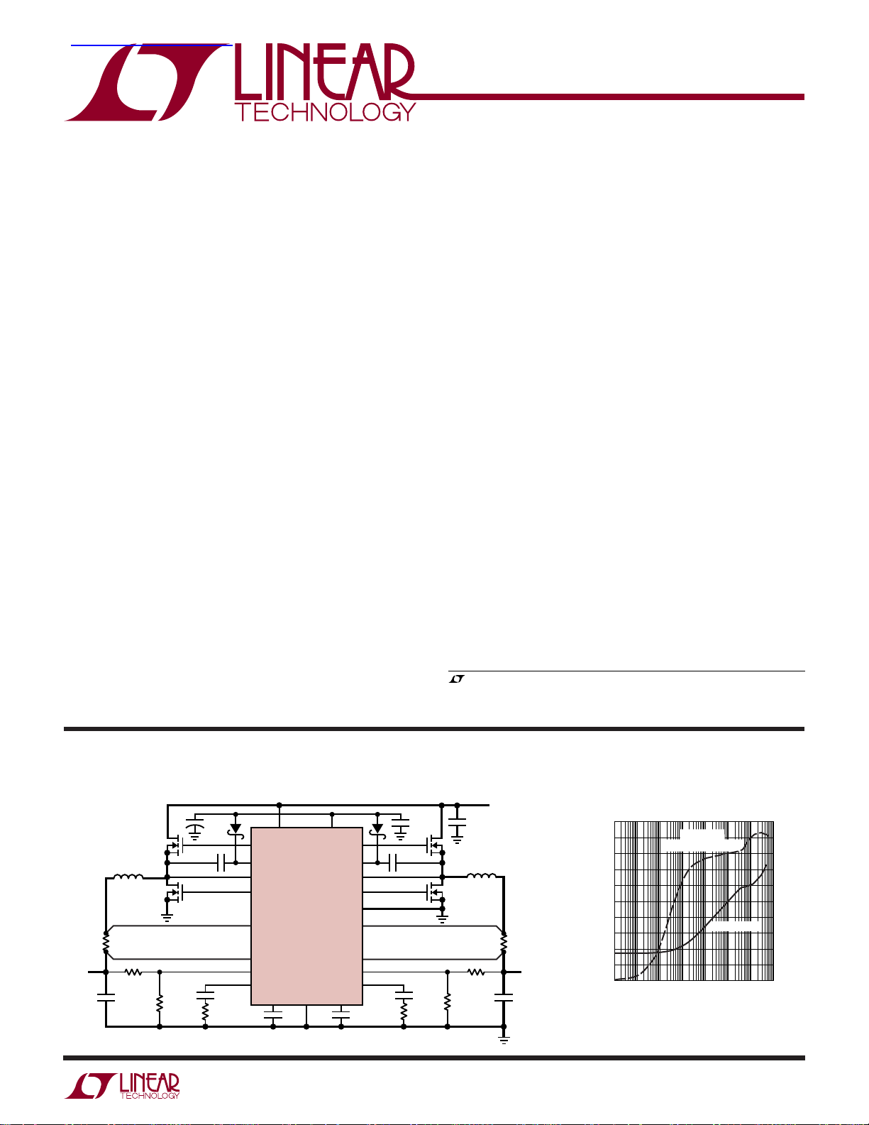
TYPICAL APPLICATIO
High Efficiency Dual 8.5V/3.3V Step-Down Converter
+
4.7µF
TG1 TG2
3.3µH
0.015Ω
V
OUT1
3.3V
5A
62.5k
150µF
20k
0.1µF
15k
BOOST1 BOOST2
SW1 SW2
BG1 BG2
SENSE1
SENSE1
V
FB1
I
TH1
220pF
TRACK/SS1 TRACK/SS2
0.1µF
V
IN
+
–
U
LTC3827-1
SGND
INTV
CC
PGND
SENSE2
SENSE2
Efficiency and Power Loss
V
IN
4V TO 36V
20k
22µF
50V
7.2µH
0.015Ω
192.5k
150µF
38271 TA01
V
8.5V
3.5A
OUT2
1µF
0.1µF
+
–
V
FB2
I
TH2
0.1µF
220pF
15k
100
90
80
70
60
50
40
EFFICIENCY (%)
30
20
10
0.001
vs Load Current
EFFICIENCY
= 12V; V
V
IN
0
0.01 0.1 1 10 100 1000 10000
LOAD CURRENT (mA)
FIGURE 13 CIRCUIT
= 3.3V
OUT
POWER LOSS
38271 TA01b
100000
10000
POWER LOSS (mW)
1000
100
10
1
0.1
38271f
1
LTC3827-1
PACKAGE/ORDER I FOR ATIO
UU
W
WWWU
ABSOLUTE AXI U RATI GS
(Note 1)
Input Supply Voltage (VIN).........................36V to –0.3V
Top Side Driver Voltages
(BOOST1, BOOST2)...............................42V to – 0.3V
Switch Voltage (SW1, SW2) .........................36V to – 5V
(BOOST1-SW1), (BOOST2-SW2) ............... 8.5V to – 0.3V
RUN1, RUN2 .............................................. 7V to –0.3V
SENSE1
PLLIN/MODE, PLLLPF, TRACK/SS1, TRACK/SS2
EXTV
I
TH1, ITH2
PGOOD1 Voltage ...................................... 8.5V to –0.3V
Peak Output Current <10µs (TG1, TG2, BG1, BG2) ... 3A
INTVCC Peak Output Current ................................ 50mA
Operating Temperature Range (Note 2) .. – 40°C to 85°C
Junction Temperature (Note 3)............................. 125°C
Storage Temperature Range ................. –65°C to 150°C
Lead Temperature (Soldering, 10 sec).................. 300°C
+
, SENSE2+, SENSE1–,
–
SENSE2
Voltages ................................11V to –0.3V
Voltages .......................................... INTV
......................................................10V to –0.3V
CC
, V
, V
FB1
Voltages ..................2.7V to –0.3V
FB2
to –0.3V
CC
TOP VIEW
1
I
TH1
2
V
FB1
+
SENSE1
SENSE1
PLLIN/MODE
SENSE2
SENSE2
TRACK/SS2
3
–
4
5
PLLLPF
6
7
SGND
8
RUN1
9
RUN2
–
10
+
11
12
V
FB2
13
I
TH2
14
28-LEAD PLASTIC SSOP
T
JMAX
G PACKAGE
= 125°C, θJA = 95°C/W
ORDER PART NUMBER
LTC3827EG-1
TRACK/SS1
28
PGOOD1
27
TG1
26
SW1
25
BOOST1
24
BG1
23
V
22
IN
PGND
21
EXTV
20
CC
INTV
19
CC
BG2
18
BOOST2
17
SW2
16
TG2
15
G PART MARKING
LTC3827EG-1
Order Options Tape and Reel: Add #TR
Lead Free: Add #PBF Lead Free Tape and Reel: Add #TRPBF
Lead Free Part Marking: http://www.linear.com/leadfree/
Consult LTC Marketing for parts specified with wider operating temperature ranges.
ELECTRICAL CHARACTERISTICS
temperature range, otherwise specifications are at T
The ● denotes the specifications which apply over the full operating
= 25°C. VIN = 12V, V
A
RUN/SS1, 2
= 5V unless otherwise noted.
SYMBOL PARAMETER CONDITIONS MIN TYP MAX UNITS
Main Control Loops
V
FB1, 2
I
VFB1, 2
V
REFLNREG
V
LOADREG
g
m1, 2
I
Q
UVLO Undervoltage Lockout VIN Ramping Down
V
OVL
I
SENSE
DF
MAX
Regulated Feedback Voltage (Note 4); I
Voltage = 1.2V
TH1, 2
●
0.792 0.800 0.808 V
Feedback Current (Note 4) –5 –50 nA
Reference Voltage Line Regulation VIN = 4V to 30V (Note 4) 0.002 0.02 %/V
Output Voltage Load Regulation (Note 4)
Transconductance Amplifier g
Measured in Servo Loop; ∆I
Measured in Servo Loop; ∆I
I
m
= 1.2V; Sink/Source 5µA (Note 4) 1.55 mmho
TH1, 2
Voltage = 1.2V to 0.7V
TH
Voltage = 1.2V to 2V
TH
●
●
0.1 0.5 %
–0.1 –0.5 %
Input DC Supply Current (Note 5)
Sleep Mode (Channel 1 On) RUN1 = 5V, RUN2 = 0V, V
Sleep Mode (Channel 2 On) RUN1 = OV, RUN2 = 5V, V
Shutdown V
Sleep Mode (Both Channels) RUN1,2 = 5V, V
Feedback Overvoltage Lockout Measured at V
Sense Pins Total Source Current (Each Channel) V
= 0V 8 20 µA
RUN1, 2
= V
FB1
, Relative to Regulated V
FB1, 2
SENSE1–, 2–
= 0.83V (No Load) 80 125 µA
FB1
= 0.83V (No Load) 80 125 µA
FB2
= 0.83V 115 160 µA
FB2
= V
SENSE1+, 2+
●
FB1, 2
81012 %
= 0V –660 µA
3.5 4 V
Maximum Duty Factor In Dropout 98 99.4 %
38271f
2
LTC3827-1
ELECTRICAL CHARACTERISTICS
temperature range, otherwise specifications are at T
The ● denotes the specifications which apply over the full operating
= 25°C. VIN = 12V, V
A
RUN/SS1, 2
= 5V unless otherwise noted.
SYMBOL PARAMETER CONDITIONS MIN TYP MAX UNITS
I
TRACK/SS1, 2
V
RUN1, 2
V
SENSE(MAX)
Soft-Start Charge Current V
ON RUN Pin ON Threshold V
Maximum Current Sense Threshold V
TRACK1, 2
RUN1, VRUN2
= 0.7V,V
FB1, 2
= 0.7V,V
V
FB1, 2
= 0V 0.75 1.0 1.35 µA
Rising 0.5 0.7 0.9 V
–
SENSE1–, 2
SENSE1–, 2
= 3.3V 90 100 110 mV
–
= 3.3V
●
80 100 115 mV
TG Transition Time: (Note 6)
TG1, 2 t
TG1, 2 t
Rise Time C
r
Fall Time C
f
= 3300pF 50 90 ns
LOAD
= 3300pF 50 90 ns
LOAD
BG Transition Time: (Note 6)
BG1, 2 t
BG1, 2 t
TG/BG t
Rise Time C
r
Fall Time C
f
Top Gate Off to Bottom Gate On Delay C
1D
= 3300pF 40 90 ns
LOAD
= 3300pF 40 80 ns
LOAD
= 3300pF Each Driver 70 ns
LOAD
Synchronous Switch-On Delay Time
BG/TG t
Bottom Gate Off to Top Gate On Delay C
2D
= 3300pF Each Driver 70 ns
LOAD
Top Switch-On Delay Time
t
ON(MIN)
Minimum On-Time (Note 7) 180 ns
INTVCC Linear Regulator
V
INTVCCVIN
V
LDOVIN
V
INTVCCEXT
V
LDOEXT
V
EXTVCC
V
LDOHYS
Internal VCC Voltage 8.5V < VIN < 30V, V
INTVCC Load Regulation ICC = 0mA to 20mA, V
Internal VCC Voltage V
= 8.5V 7.2 7.5 7.8 V
EXTVCC
INTVCC Load Regulation ICC = 0mA to 20mA, V
EXTVCC Switchover Voltage ICC = 20mA, EXTV
= 0V 5.0 5.25 5.5 V
EXTVCC
= 0V 0.2 1.0 %
EXTVCC
= 8.5V 0.2 1.0 %
EXTVCC
Ramping Positive 4.5 4.7 V
CC
EXTVCC Hysteresis 0.2 V
Oscillator and Phase-Locked Loop
f
NOM
f
LOW
f
HIGH
f
SYNCMIN
f
SYNCMAX
I
PLLLPF
Nominal Frequency V
Lowest Frequency V
Highest Frequency V
= Floating; PLLIN/MODE = DC Voltage 360 400 440 kHz
PLLLPF
= 0V; PLLIN/MODE = DC Voltage 220 250 280 kHz
PLLLPF
= INTVCC; PLLIN/MODE = DC Voltage 475 530 580 kHz
PLLLPF
Minimum Synchronizable Frequency PLLIN/MODE = External Clock; V
Maximum Synchronizable Frequency PLLIN/MODE = External Clock; V
Phase Detector Output Current
Sinking Capability f
Sourcing Capability f
PLLIN/MODE
PLLIN/MODE
< f
> f
OSC
OSC
= 0V 115 140 kHz
PLLLPF
= 2V 650 800 kHz
PLLLPF
–5 µA
5 µA
PGOOD Output
V
PGL
I
PGOOD
V
PG
PGOOD Voltage Low I
PGOOD Leakage Current V
= 2mA 0.1 0.3 V
PGOOD
= 5V ±1 µA
PGOOD
PGOOD Trip Level VFB with Respect to Set Regulated Voltage
Ramping Negative –12 –10 –8 %
V
FB
V
Ramping Positive 8 10 12 %
FB
Note 1: Absolute Maximum Ratings are those values beyond which the life
of a device may be impaired.
Note 2: The LTC3827E-1 is guaranteed to meet performance specifications
from 0°C to 70°C. Specifications over the –40°C to 85°C operating
temperature range are assured by design, characterization and correlation
with statistical process controls.
Note 3: T
dissipation P
is calculated from the ambient temperature TA and power
J
according to the following formula:
D
= TA + (PD • 95 °C/W)
T
J
Note 4: The LTC3827-1 is tested in a feedback loop that servos V
a specified voltage and measures the resultant V
FB1, 2.
ITH1, 2
to
Note 5: Dynamic supply current is higher due to the gate charge being
delivered at the switching frequency. See Applications Information.
Note 6: Rise and fall times are measured using 10% and 90% levels. Delay
times are measured using 50% levels.
Note 7: The minimum on-time condition is specified for an inductor
peak-to-peak ripple current ≥40% of I
(see minimum on-time
MAX
considerations in the Applications Information section).
38271f
3
LTC3827-1
UW
TYPICAL PERFOR A CE CHARACTERISTICS
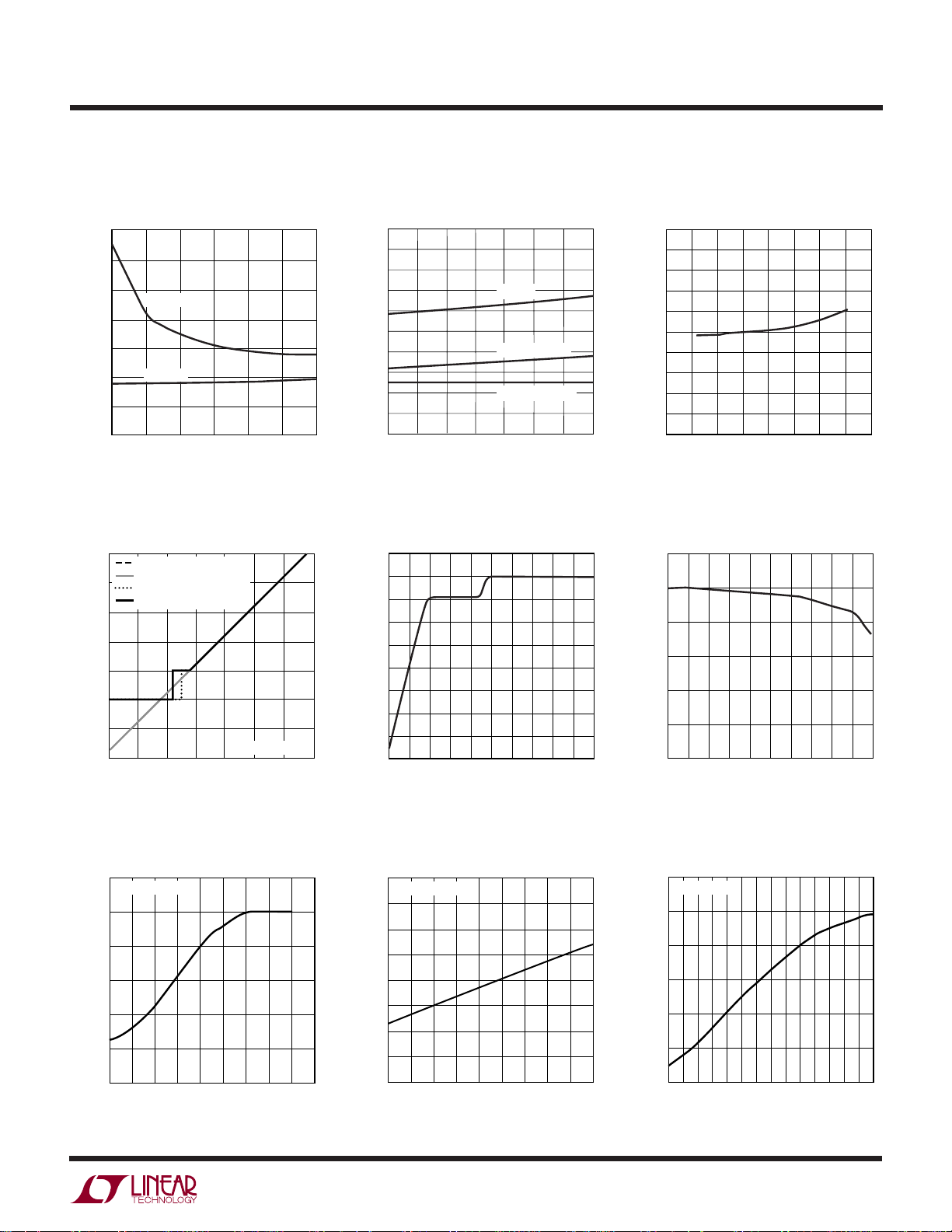
Efficiency and Power Loss
vs Output Current Efficiency vs Load Current
100
90
80
70
60
50
40
EFFICIENCY (%)
30
20
10
0
0.001
Burst Mode OPERATION
FORCED CONTINUOUS MODE
PULSE SKIPPING MODE
VIN = 12V
= 3.3V
V
OUT
0.01 0.1 1 10 100 1000 10000
LOAD CURRENT (mA)
FIGURE 13 CIRCUIT
10000
1000
100
10
1
0.1
38271 G01
100
90
POWER LOSS (mW)
80
70
EFFICIENCY (%)
60
50
40
0.001
FIGURE 13 CIRCUIT
VIN = 12V
= 5V
V
IN
= 3.3V
V
OUT
0.01 0.1 1 10 100 1000 10000
LOAD CURRENT (mA)
38271 G02
Efficiency vs Input Voltage
98
96
94
92
90
88
EFFICIENCY (%)
86
84
V
= 3.3V
OUT
82
51015203040
0
INPUT VOLTAGE (V)
FIGURE 13 CIRCUIT
25 35
38271 G03
V
100mV/DIV
COUPLED
2A/DIV
FORCED
CONTINUOUS
MODE
2A/DIV
BURST MODE
PULSE
SKIPPING
MODE
Load Step
(Burst Mode Operation)
OUT
AC
I
L
20µs/DIV
FIGURE 13 CIRCUIT
V
= 3.3V
OUT
Inductor Current at Light Load
FIGURE 13 CIRCUIT
= 3.3V
V
OUT
I
= 300µA
LOAD
4µs/DIV
38271 G04
38271 G07
V
OUT
100mV/DIV
AC
COUPLED
2A/DIV
Load Step
(Forced Continuous Mode)
I
L
20µs/DIV
FIGURE 13 CIRCUIT
= 3.3V
V
OUT
Soft Start-Up
FIGURE 13 CIRCUIT
20ms/DIV
38271 G05
V
OUT2
2V/DIV
V
OUT1
2V/DIV
38271 G08
V
OUT
100mV/DIV
AC
COUPLED
2A/DIV
Load Step
(Pulse Skip Mode)
I
L
20µs/DIV
FIGURE 13 CIRCUIT
V
= 3.3V
OUT
Tracking Start-Up
FIGURE 13 CIRCUIT
20ms/DIV
38271 G06
V
OUT2
2V/DIV
V
OUT1
2V/DIV
38271 G09
4
38271f
UW
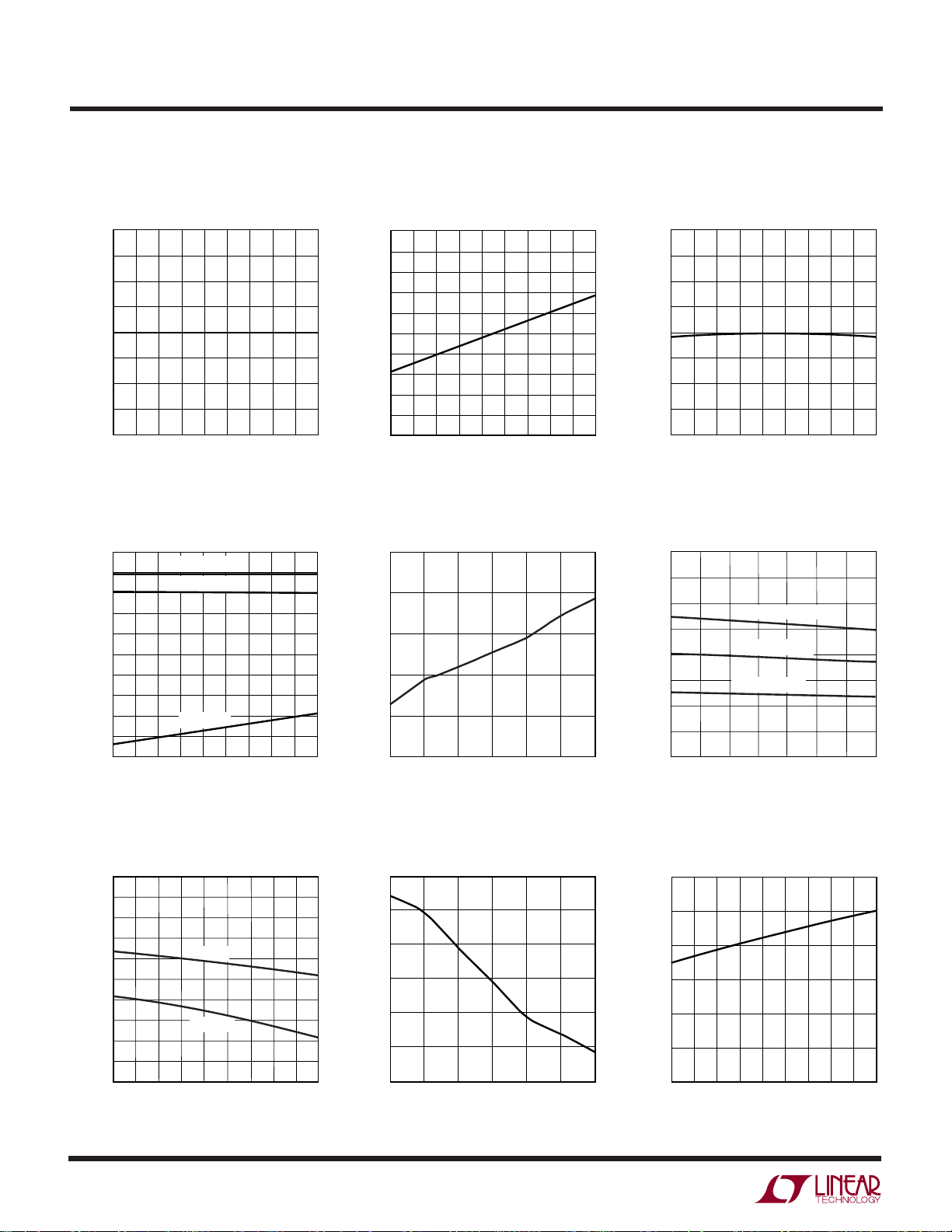
DUTY CYCLE (%)
0
CURRENT SENSE THRESHOLD (mV)
40
80
120
20
60
100
20 40 60 80
38271 G15
10010030507090
TYPICAL PERFOR A CE CHARACTERISTICS
LTC3827-1
Total Input Supply Current
vs Input Voltage
350
300
250
200
150
100
SUPPLY CURRENT (µA)
50
300µA LOAD
NO LOAD
0
5
10 15
20 30
INPUT VOLTAGE (V)
FIGURE 13 CIRCUIT
Maximum Current Sense Voltage
Voltage
vs I
TH
100
–20
CURRENT SENSE THRESHOLD (mV)
–40
PULSE SKIPPING
FORCED CONTINUOUS
80
BURST MODE (RISING)
BURST MODE (FALLING)
60
40
20
0
0
0.2 0.4
10% Duty Cycle
0.8 1.2 1.4
0.6 1.0
ITH PIN VOLTAGE (V)
25 35
38271 G10
38271 G13
EXTVCC Switchover and INTV
Voltages vs Temperature
6.0
5.8
5.6
5.4
5.2
VOLTAGES (V)
CC
5.0
4.8
4.6
AND INTV
CC
4.4
EXTV
4.2
4.0
–45
–25
15
–5
TEMPERATURE (°C)
Sense Pins Total Input
Bias Current
200
100
0
–100
–200
–300
–400
INPUT CURRENT (µA)
–500
–600
–700
12345 10
0
V
COMMON MODE VOLTAGE (V)
SENSE
INTVCC
EXTVCC RISING
EXTVCC FALLING
35
55
6789
CC
75 95
38271 G11
38271 G14
Line Regulation
INTV
CC
5.50
5.45
5.40
5.35
5.30
5.25
VOLTAGE (V)
5.20
CC
5.15
INTV
5.10
5.05
5.00
0
515
10
INPUT VOLTAGE (V)
Maximum Current Sense
Threshold vs Duty Cycle
35
20
30
25
40
38271 G12
Foldback Current Limit Quiescent Current vs Temperature
120
TRACK/SS = 1V
100
80
60
40
20
MAXIMUM CURRENT SENSE VOLTAGE (V)
0
0.1 0.3
0.2
0
FEEDBACK VOLTAGE (V)
0.7
0.5 0.9
0.6
0.4
0.8
38271 G16
100
PLLIN/MODE = 0V
95
90
85
80
75
70
QUIESCENT CURRENT (µA)
65
60
–30 90
–45
–15
15
0
TEMPERATURE (°C)
SENSE Pins Total Input
Bias Current vs I
12
V
= 3.3V
SENSE
10
8
6
4
INPUT CURRENT (µA)
2
0
30
75
45
60
38271 G17
0
0.2
TH
0.4 0.6 0.8 1 1.2 1.4
ITH VOLTAGE (V)
38271 G18
38271f
5
LTC3827-1
UW
TYPICAL PERFOR A CE CHARACTERISTICS
TRACK/SS Pull-Up Current
vs Temperature
1.20
1.15
1.10
1.05
1.00
0.95
TRACK/SS CURRENT (µA)
0.90
0.85
0.80
–30 90
–45
–15
15
30
0
TEMPERATURE (°C)
Sense Pins Total Input Current
vs Temperature
INPUT CURRENT (µA)
200
100
–100
–200
–300
–400
–500
–600
–700
–800
0
–45
–30 0
V
= 10V
OUT
V
= 3.3V
OUT
V
= OV
OUT
–15
15
TEMPERATURE (°C)
30 90
Shutdown (RUN) Threshold
vs Temperature
1.00
0.95
0.90
0.85
0.80
0.75
0.70
0.65
RUN PIN VOLTAGE (V)
0.60
0.55
75
45
60
38271 G19
0.50
–30 90
–45
–15
15
30
0
TEMPERATURE (°C)
75
45
60
38271 G20
Shutdown Current
vs Input Voltage
25
20
15
10
INPUT CURRENT (µA)
5
60
75
45
38271 G22
0
510
25
20
15
INPUT VOLTAGE (V)
30
35
38271 G23
Regulated Feedback Voltage
vs Temperature
808
806
804
802
800
798
796
794
REGULATED FEEDBACK VOLTAGE (mV)
792
–30 90
–45
–15
15
30
0
TEMPERATURE (°C)
Oscillator Frequency
vs Temperature
800
700
600
500
400
300
FREQUENCY (kHz)
200
100
0
–45
–25
–5
V
= INTVCC
PLLLPF
V
= FLOAT
PLLLPF
V
= GND
PLLLPF
35
15
TEMPERATURE (°C)
75
45
60
38271 G21
75 95
38271 G24
55
Undervoltage Lockout Threshold
vs Temperature
4.2
4.1
4.0
3.9
3.8
3.7
VOLTAGE (V)
3.6
CC
3.5
INTV
3.4
3.3
3.2
–45
–30
RISING
FALLING
15
0
–15
TEMPERATURE (°C)
6
Oscillator Frequency
vs Input Voltage
404
402
400
398
396
FREQUENCY (kHz)
394
30
604575 90
38271 G25
392
510
15
INPUT VOLTAGE (V)
25
20
30
35
38271 G26
Shutdown Current
vs Temperature
12
10
8
6
4
SHUTDOWN CURRENT (µA)
2
0
–30 90
–45
–15
15
0
TEMPERATURE (°C)
30
75
45
60
38271 G27
38271f

LTC3827-1
U
UU
PI FU CTIO S
I
TH1, ITH2
Switching Regulator Compensation Points. Each associated channel’s current comparator trip point increases
with this control voltage.
V
FB1
feedback voltage for each controller from an external
resistive divider across the output.
SENSE1
Differential Current Comparators. The I
controlled offsets between the SENSE
in conjunction with R
SENSE1
Differential Current Comparators.
PLLLPF (Pin 5): The phase-locked loop’s lowpass filter
is tied to this pin when synchronizing to an external
clock. Alternatively, tie this pin to GND, INTV
floating to select 250kHz, 530kHz or 400kHz switching
frequency.
PLLIN/MODE (Pin 6): External Synchronization Input to
Phase Detector and Forced Continuous Control Input. When
an external clock is applied to this pin, the phase-locked
loop will force the rising TG1 signal to be synchronized
with the rising edge of the external clock. In this case, an
R-C filter must be connected to the PLLLPF pin. When not
synchronizing to an external clock, this input, which acts
on both controllers, determines how the LTC3827-1 operates at light loads. Pulling this pin below 0.7V selects Burst
Mode operation. Tying this pin to INTV
ous inductor current operation. Tying this pin to a voltage
greater than 0.9V and less than INTV
skipping operation.
SGND (Pin 7): Small Signal Ground common to both
controllers, must be routed separately from high current
grounds to the common (–) terminals of the C
RUN1, RUN2 (Pins 8, 9): Digital Run Control Inputs for
Each Controller. Forcing either of these pins below 0.7V
shuts down that controller. Forcing both of these pins
below 0.7V shuts down the entire LTC3827-1, reducing
quiescent current to approximately 8µA.
INTV
Regulator. The driver and control circuits are powered from
(Pins 1, 13): Error Amplifier Outputs and
, V
(Pins 2, 12): Receives the remotely sensed
FB2
+
, SENSE2+ (Pins 3, 11): The (+) Input to the
pin voltage and
TH
–
and SENSE+ pins
set the current trip threshold.
SENSE
–
, SENSE2– (Pins 4, 10): The (–) Input to the
or leave
CC
forces continu-
CC
–0.5V selects pulse
CC
capacitors.
IN
(Pin 19): Output of the Internal Linear Low Dropout
CC
this voltage source. Must be decoupled to power ground with
a minimum of 4.7µF tantalum or other low ESR capacitor.
EXTV
Connected to INTV
bypassing the internal
EXTV
(Pin 20): External Power Input to an Internal LDO
CC
. This LDO supplies INTVCC power,
CC
LDO powered from VIN whenever
is higher than 4.7V. See EXTVCC Connection in the
CC
Applications Information section. Do not exceed 10V on
this pin.
PGND (Pin 21): Driver Power Ground. Connects to the
sources of bottom (synchronous) N-channel MOSFETs, anodes of the Schottky rectifiers and the (–) terminal(s) of C
IN
.
VIN (Pin 22): Main Supply Pin. A bypass capacitor should
be tied between this pin and the signal ground pin.
BG1, BG2 (Pins 23, 18): High Current Gate Drives for
Bottom (Synchronous) N-Channel MOSFETs. Voltage
swing at these pins is from ground to INTV
CC
.
BOOST1, BOOST2 (Pins 24, 17): Bootstrapped Supplies
to the Top Side Floating Drivers. Capacitors are connected
between the BOOST and SW pins and Schottky diodes are
tied between the BOOST and INTV
at the BOOST pins is from INTV
pins. Voltage swing
CC
to (VIN + INTVCC).
CC
SW1, SW2 (Pins 25, 16): Switch Node Connections to
Inductors. Voltage swing at these pins is from a Schottky
diode (external) voltage drop below ground to VIN.
TG1, TG2 (Pins 26, 15): High Current Gate Drives for Top
N-Channel MOSFETs. These are the outputs of floating
drivers with a voltage swing equal to INTV
CC
– 0.5V
superimposed on the switch node voltage SW.
PGOOD1 (Pin 27): Open-Drain Logic Output. PGOOD1 is
pulled to ground when the voltage on the V
pin is not
FB1
within ±10% of its set point.
TRACK/SS1, TRACK/SS2 (Pins 28, 14): External Tracking
and Soft-Start Input. The LTC3827-1 regulates the V
FB1,2
voltage to the smaller of 0.8V or the voltage on the TRACK/
SS1,2 pin. A internal 1µA pull-up current source is con-
nected to this pin. A capacitor to ground at this pin sets the
ramp time to final regulated output voltage. Alternatively,
a resistor divider on another voltage supply connected to
this pin allows the LTC3827-1 output to track the other
supply during startup.
38271f
7
LTC3827-1
U
U
W
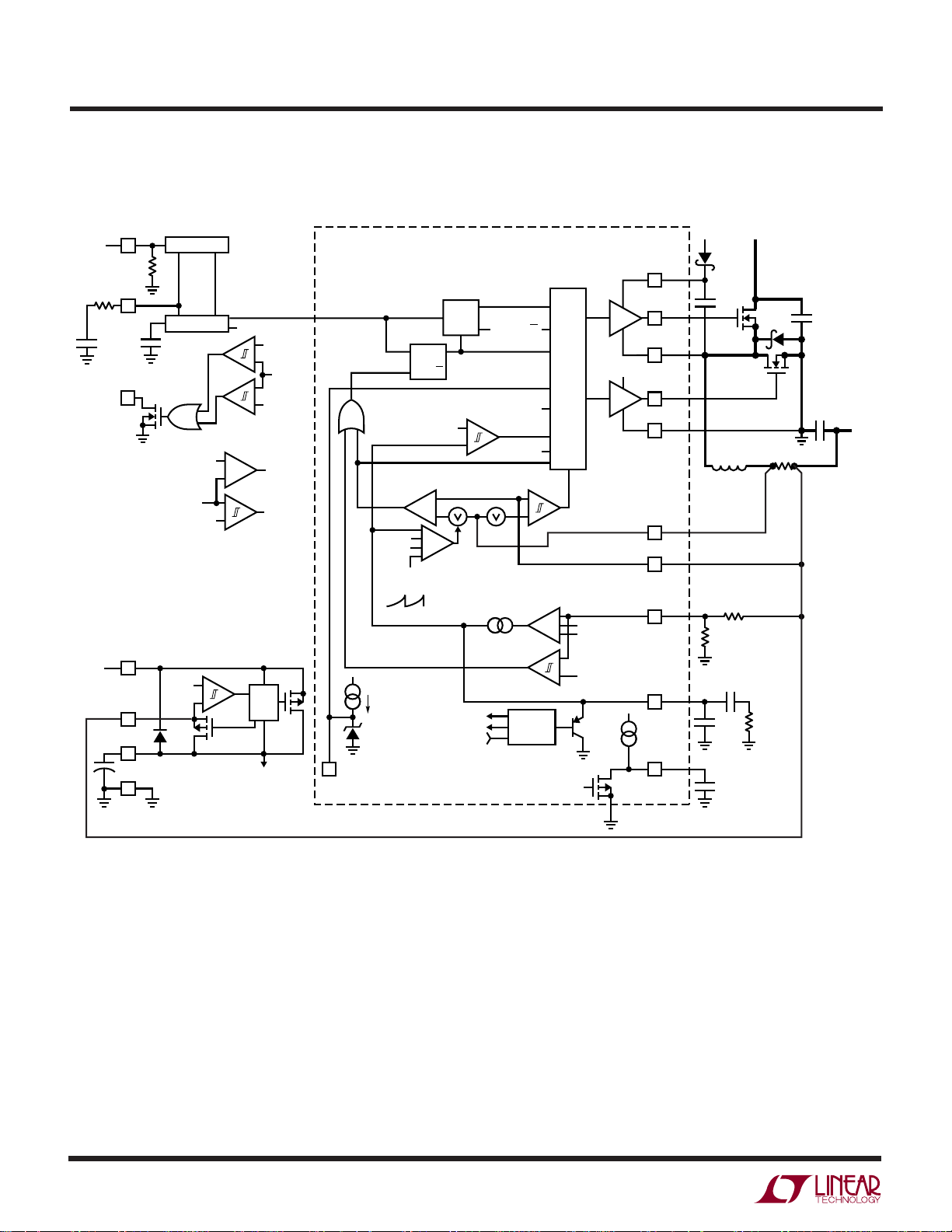
FU CTIO AL DIAGRA
PLLIN/MODE
F
6
IN
PLLLPF
5
R
LP
C
LP
PGOOD1
27
V
IN
22
V
IN
EXTV
20
INTV
19
+
SGND
7
PLLIN/MODE
CC
CC
PHASE DET
100k
OSCILLATOR
INTVCC-0.5V
4.7V
0.8V
CLK1
CLK2
–
0.88V
+
V
FB1
–
+
0.72V
–
FC
+
–
BURSTEN
+
+
–
5V/
7.5V
LDO
INTERNAL
SUPPLY
DUPLICATE FOR SECOND
CONTROLLER CHANNEL
ICMP IR
0.45V
2(VFB)
SLOPE
COMP
0.5µA
6V
RUN
8, 9
SRQ
+
–
Q
0.4V
DROP
OUT
DET
+
–
+– –+
SHDN
RST
2(VFB)
BOT
B
6mV
TOP ON
BURSTEN
SLEEP
SHDN
FOLDBACK
INTV
BOOST
24, 17
INTV
CC
PGND
SENSE
SENSE
V
TRACK/SS
TG
SW
BG
I
26, 15
25, 16
23, 18
21
+
3, 11
–
4, 10
FB
2, 12
TH
1,13
28,14
TOP
FC
SWITCH
LOGIC
BOT
–
+
V
FB
–
TRACK/SS
EA
+
0.80V
OV
+
–
0.88V
1µA
SHDN
V
CC
IN
D
B
C
B
L
R
B
R
A
C
C
R
C
C
C2
C
SS
D
R
SENSE
C
IN
C
OUT
V
OUT
8
38271 FD
38271f

OPERATIO
LTC3827-1
U
(Refer to Functional Diagram)
Main Control Loop
The LTC3827-1 uses a constant frequency, current mode
step-down architecture with the two controller channels
operating 180 degrees out of phase. During normal operation, each external top MOSFET is turned on when the
clock for that channel sets the RS latch, and is turned off
when the main current comparator, I
latch. The peak inductor current at which I
resets the latch is controlled by the voltage on the I
, resets the RS
CMP
trips and
CMP
TH
pin,
which is the output of the error amplifier EA. The error
amplifier compares the output voltage feedback signal at
the V
divider connected across the output voltage, V
pin, (which is generated with an external resistor
FB
, to
OUT
ground) to the internal 0.800V reference voltage. When
the load current increases, it causes a slight decrease in
V
relative to the reference, which causes the EA to
FB
increase the I
voltage until the average inductor current
TH
matches the new load current.
After the top MOSFET is turned off each cycle, the bottom
MOSFET is turned on until either the inductor current
starts to reverse, as indicated by the current comparator
IR, or the beginning of the next clock cycle.
INTV
/EXTVCC Power
CC
Power for the top and bottom MOSFET drivers and most
other internal circuitry is derived from the INTV
CC
pin.
When the EXTVCC pin is left open or tied to a voltage less
than 4.7V, an internal 5V low dropout linear regulator
supplies INTV
power from VIN. If EXTVCC is taken above
CC
4.7V, the 5V regulator is turned off and a 7.5V low dropout
linear regulator is enabled that supplies INTV
from EXTV
. If EXTVCC is less than 7.5V (but greater than
CC
4.7V), the 7.5V regulator is in dropout and INTV
approximately equal to EXTV
. When EXTVCC is greater
CC
power
CC
CC
is
than 7.5V (up to an absolute maximum rating of 10V),
INTV
is regulated to 7.5V. Using the EXTVCC pin allows
CC
the INTVCC power to be derived from a high efficiency
external source such as one of the LTC3827-1 switching
regulator outputs.
Each top MOSFET driver is biased from the floating bootstrap capacitor C
, which normally recharges during each
B
off cycle through an external diode when the top MOSFET
turns off. If the input voltage V
decreases to a voltage
IN
close to V
, the loop may enter dropout and attempt to
OUT
turn on the top MOSFET continuously. The dropout detector detects this and forces the top MOSFET off for about
one twelfth of the clock period every tenth cycle to allow C
B
to recharge.
Shutdown and Start-Up (RUN1, RUN2 and TRACK/
SS1, TRACK/SS2 Pins)
The two channels of the LTC3827-1 can be independently
shut down using the RUN1 and RUN2 pins. Pulling either
of these pins below 0.7V shuts down the main control loop
for that controller. Pulling both pins low disables both
controllers and most internal circuits, including the
INTV
regulator, and the LTC3827-1 draws only 8µA of
CC
quiescent current.
Releasing either RUN pin allows an internal 0.5µA current
to pull up the pin and enable that controller. Alternatively,
the RUN pin may be externally pulled up or driven directly
by logic. Be careful not to exceed the Absolute Maximum
rating of 6V on this pin.
The start-up of each controller’s output voltage V
OUT
is controlled by the voltage on the TRACK/SS1 and TRACK/SS2
pin. When the voltage on the TRACK/SS pin is less than the
0.8V internal reference, the LTC3827-1 regulates the V
FB
voltage to the TRACK/SS pin voltage instead of the 0.8V
reference. This allows the TRACK/SS pin to be used to
program a soft start by connecting an external capacitor
from the TRACK/SS pin to SGND. An internal 1µA pull-up
current charges this capacitor creating a voltage ramp on
the TRACK/SS pin. As the TRACK/SS voltage rises linearly
from 0V to 0.8V (and beyond), the output voltage V
OUT
rises smoothly from zero to its final value.
Alternatively the TRACK/SS pin can be used to cause the
startup of V
to “track” that of another supply. Typically,
OUT
this requires connecting to the TRACK/SS pin an external
resistor divider from the other supply to ground (see
Applications Information section).
When the corresponding RUN pin is pulled low to disable
a controller, or when V
drops below its undervoltage
IN
lockout threshold of 3.7V, the TRACK/SS pin is pulled low
by an internal MOSFET. When in undervoltage lockout,
both controllers are disabled and the external MOSFETs
are held off.
38271f
9

LTC3827-1
OPERATIO
U
(Refer to Functional Diagram)
Light Load Current Operation (Burst Mode Operation,
Pulse Skipping, or Continuous Conduction)
(PLLIN/MODE Pin)
The LTC3827-1 can be enabled to enter high efficiency
Burst Mode operation, constant frequency pulse skipping
mode, or forced continuous conduction mode at low load
currents. To select Burst Mode operation, tie the PLLIN/
MODE pin to a DC voltage below 0.8V (e.g., SGND). To
select forced continuous operation, tie the PLLIN/MODE
pin to INTV
PLLIN/MODE pin to a DC voltage greater than 0.8V and
less than INTV
When a controller is enabled for Burst Mode operation,
the peak current in the inductor is set to approximately
one-tenth of the maximum sense voltage even though
the voltage on the I
average inductor current is lower than the load current,
the error amplifier EA will decrease the voltage on the
ITH pin. When the ITH voltage drops below 0.4V, the
internal sleep signal goes high (enabling “sleep” mode)
and both external MOSFETs are turned off. The I
is then disconnected from the output of the EA and
“parked” at 0.425V.
In sleep mode, much of the internal circuitry is turned
off, reducing the quiescent current that the LTC3827-1
draws. If one channel is shut down and the other
channel is in sleep mode, the LTC3827-1 draws only
80µA of quiescent current. If both channels are in sleep
mode, the LTC3827-1 draws only 115µA of quiescent
current. In sleep mode, the load current is supplied by
the output capacitor. As the output voltage decreases,
the EA’s output begins to rise. When the output voltage
drops enough, the ITH pin is reconnected to the output
of the EA, the sleep signal goes low, and the controller
. To select pulse-skipping mode, tie the
CC
– 0.5V.
CC
pin indicates a lower value. If the
TH
pin
TH
resumes normal operation by turning on the top external MOSFET on the next cycle of the internal oscillator.
When a controller is enabled for Burst Mode operation, the
inductor current is not allowed to reverse. The reverse
current comparator (IR) turns off the bottom external
MOSFET just before the inductor current reaches zero,
preventing it from reversing and going negative. Thus, the
controller operates in discontinuous operation.
In forced continuous operation, the inductor current is
allowed to reverse at light loads or under large transient
conditions. The peak inductor current is determined by the
voltage on the I
mode, the efficiency at light loads is lower than in Burst
Mode operation. However, continuous has the advantages
of lower output ripple and less interference to audio
circuitry. In forced continuous mode, the output ripple is
independent of load current.
When the PLLIN/MODE pin is connected for pulse-skipping mode or clocked by an external clock source to use
the phase-locked loop (see Frequency Selection and PhaseLocked Loop section), the LTC3827-1 operates in PWM
pulse skipping mode at light loads. In this mode, constant
frequency operation is maintained down to approximately
1% of designed maximum output current. At very light
loads, the current comparator I
several cycles and force the external top MOSFET to stay
off for the same number of cycles (i.e., skipping pulses).
The inductor current is not allowed to reverse (discontinuous operation). This mode, like forced continuous operation, exhibits low output ripple as well as low audio noise
and reduced RF interference as compared to Burst Mode
operation. It provides higher low current efficiency than
forced continuous mode, but not nearly as high as Burst
Mode operation.
pin, just as in normal operation. In this
TH
may remain tripped for
CMP
10
38271f

OPERATIO
LTC3827-1
U
(Refer to Functional Diagram)
Frequency Selection and Phase-Locked Loop (PLLLPF
and PLLIN/MODE Pins)
The selection of switching frequency is a tradeoff between
efficiency and component size. Low frequency operation
increases efficiency by reducing MOSFET switching losses,
but requires larger inductance and/or capacitance to maintain low output ripple voltage.
The switching frequency of the LTC3827-1’s controllers
can be selected using the PLLLPF pin.
If the PLLIN/MODE pin is not being driven by an external
clock source, the PLLLPF pin can be floated, tied to
INTV
250kHz, respectively.
A phase-locked loop (PLL) is available on the LTC3827-1
to synchronize the internal oscillator to an external clock
source that is connected to the PLLIN/MODE pin. In this
case, a series R-C should be connected between the
PLLLPF pin and SGND to serve as the PLL’s loop filter. The
LTC3827-1 phase detector adjusts the voltage on the
PLLLPF pin to align the turn-on of controller 1’s external
top MOSFET to the rising edge of the synchronizing signal.
Thus, the turn-on of controller 2’s external top MOSFET is
180 degrees out of phase to the rising edge of the external
clock source.
The typical capture range of the LTC3827-1’s phaselocked loop is from approximately 115kHz to 800kHz, with
a guarantee over all manufacturing variations to be between 140kHz and 650kHz. In other words, the LTC38271’s PLL is guaranteed to lock to an external clock source
whose frequency is between 140kHz and 650kHz.
The typical input clock thresholds on the PLLIN/MODE pin
are 1.6V (rising) and 1.2V (falling).
, or tied to SGND to select 400kHz, 530kHz, or
CC
Output Overvoltage Protection
An overvoltage comparator guards against transient overshoots as well as other more serious conditions that may
overvoltage the output. When the V
10% above its regulation point of 0.800V, the top MOSFET
is turned off and the bottom MOSFET is turned on until the
overvoltage condition is cleared.
Power Good (PGOOD1) Pin
The PGOOD1 pin is connected to an open drain of an
internal N-channel MOSFET. The MOSFET turns on and
pulls the PGOOD1 pin low when the V
within ±10% of the 0.8V reference voltage. The PGOOD1
pin is also pulled low when the RUN1 pin is low (shut
down) or when the LTC3827-1 is in undervoltage lockout.
When the V
the MOSFET is turned off and the pin is allowed to be pulled
up by an external resistor to a source of up to 8.5V.
THEORY AND BENEFITS OF 2-PHASE OPERATION
Why the need for 2-phase operation? Up until the 2-phase
family, constant-frequency dual switching regulators operated both channels in phase (i.e., single-phase operation). This means that both switches turned on at the same
time, causing current pulses of up to twice the amplitude
of those for one regulator to be drawn from the input
capacitor and battery. These large amplitude current pulses
increased the total RMS current flowing from the input
capacitor, requiring the use of more expensive input
capacitors and increasing both EMI and losses in the input
capacitor and battery.
With 2-phase operation, the two channels of the dualswitching regulator are operated 180 degrees out of
phase. This effectively interleaves the current pulses
drawn by the switches, greatly reducing the overlap time
where they add together.
pin voltage is within the ±10% requirement,
FB1
The result is a significant reduc-
pin rises more than
FB
pin voltage is not
FB1
tion in total RMS input current, which in turn allows less
expen
sive input capacitors to be used, reduces shielding
requirements for EMI and improves real world operating
efficiency.
38271f
11

LTC3827-1
OPERATIO
Figure 1. Input Waveforms Comparing Single-Phase (a) and 2-Phase (b) Operation for Dual Switching Regulators
Converting 12V to 5V and 3.3V at 3A Each. The Reduced Input Ripple with the 2-Phase Regulator Allows
Less Expensive Input Capacitors, Reduces Shielding Requirements for EMI and Improves Efficiency
U
(Refer to Functional Diagram)
I
= 2.53A
IN(MEAS)
RMS
(a)
38271 F01a
5V SWITCH
20V/DIV
3.3V SWITCH
20V/DIV
INPUT CURRENT
5A/DIV
INPUT VOLTAGE
500mV/DIV
I
IN(MEAS)
= 1.55A
(b)
38271 F01b
RMS
Figure 1 compares the input waveforms for a representative single-phase dual switching regulator to the
LTC3827-1 2-phase dual switching regulator. An actual measure-ment of the RMS input current under
these conditions shows that 2-phase operation dropped
the input current from 2.53A
to 1.55A
RMS
RMS
. While
this is an impressive reduction in itself, remember that
the power losses are proportional to I
RMS
2
, meaning
that the actual power wasted is reduced by a factor of
2.66. The reduced input ripple voltage also means less
power is lost in the input power path, which could
include batteries, switches, trace/connector resistances
and protection circuitry. Improvements in both conducted and radiated EMI also directly accrue as a result
of the reduced RMS input current and voltage.
Of course, the improvement afforded by 2-phase operation is a function of the dual switching regulator’s relative
3.0
2.5
2.0
duty cycles which, in turn, are dependent upon the input
voltage V
(Duty Cycle = V
IN
OUT/VIN
). Figure 2 shows how
the RMS input current varies for single-phase and 2-phase
operation for 3.3V and 5V regulators over a wide input
voltage range.
It can readily be seen that the advantages of 2-phase
operation are not just limited to a narrow operating range,
for most applications is that 2-phase operation will reduce
the input capacitor requirement to that for just one channel
operating at maximum current and 50% duty cycle.
The schematic on the first page is a basic LTC3827-1
application circuit. External component selection is driven
by the load requirement, and begins with the selection of
R
are selected. Finally, CIN and C
SINGLE PHASE
DUAL CONTROLLER
and the inductor value. Next, the power MOSFETs
SENSE
are selected.
OUT
12
1.5
1.0
INPUT RMS CURRENT (A)
0.5
VO1 = 5V/3A
= 3.3V/3A
V
O2
0
0
2-PHASE
DUAL CONTROLLER
10 20 30 40
INPUT VOLTAGE (V)
38271 F02
Figure 2. RMS Input Current Comparison
38271f

WUUU
APPLICATIO S I FOR ATIO
LTC3827-1
R
R
Selection For Output Current
SENSE
is chosen based on the required output current.
SENSE
The current comparator has a maximum threshold of
100mV/R
and an input common mode range of
SENSE
SGND to 10V. The current comparator threshold sets the
peak of the inductor current, yielding a maximum average
output current I
peak-to-peak ripple current, ∆I
equal to the peak value less half the
MAX
.
L
Allowing a margin for variations in the IC and external
component values yields:
mV
R
SENSE
80
=
I
MAX
When using the controller in very low dropout conditions,
the maximum output current level will be reduced due to
the internal compensation required to meet stability
criterion for buck regulators operating at greater than
50% duty factor. A curve is provided in the Typical
Performance Characteristics section to estimate this reduction in peak output current level depending upon the
operating duty factor.
Operating Frequency and Synchronization
The choice of operating frequency, is a trade-off between
efficiency and component size. Low frequency operation
improves efficiency by reducing MOSFET switching losses,
both gate charge loss and transition loss. However, lower
frequency operation requires more inductance for a given
amount of ripple current.
of smaller inductor and capacitor values. So why would
anyone ever choose to operate at lower frequencies with
larger components? The answer is efficiency. A higher
frequency generally results in lower efficiency because of
MOSFET gate charge losses. In addition to this basic
trade-off, the effect of inductor value on ripple current and
low current operation must also be considered.
The inductor value has a direct effect on ripple current. The
inductor ripple current ∆I
tance or frequency and increases with higher V
∆I
1
()( )
fL
V
=
L OUT
decreases with higher induc-
L
V
OUT
V
IN
⎞
⎟
⎠
⎛
1
–
⎜
⎝
IN
:
Accepting larger values of ∆IL allows the use of low
inductances, but results in higher output voltage ripple
and greater core losses. A reasonable starting point for
setting ripple current is ∆I
=0.3(I
L
). The maximum ∆I
MAX
L
occurs at the maximum input voltage.
The inductor value also has secondary effects. The transition to Burst Mode operation begins when the average
inductor current required results in a peak current below
10% of the current limit determined by R
inductor values (higher ∆I
) will cause this to occur at
L
SENSE
. Lower
lower load currents, which can cause a dip in efficiency in
the upper range of low current operation. In Burst Mode
operation, lower inductance values will cause the burst
frequency to decrease.
Inductor Core Selection
The internal oscillator for each of the LTC3827-1’s controllers
runs at a nominal 400kHz frequency when the PLLLPF pin
is left floating and the PLLIN/MODE pin is a DC low or high.
Pulling the PLLLPF to INTV
selects 530kHz operation;
CC
pulling the PLLLPF to SGND selects 250kHz operation.
Alternatively, the LTC3827-1 will phase-lock to a clock
signal applied to the PLLIN/MODE pin with a frequency
between 140kHz and 650kHz (see Phase-Locked Loop
and Frequency Synchronization).
Inductor Value Calculation
The operating frequency and inductor selection are interrelated in that higher operating frequencies allow the use
Once the value for L is known, the type of inductor must
be selected. High efficiency converters generally cannot
afford the core loss found in low cost powdered iron
cores, forcing the use of more expensive ferrite or
molypermalloy cores. Actual core loss is independent of
core size for a fixed inductor value, but it is very dependent
on inductance selected. As inductance increases, core
losses go down. Unfortunately, increased inductance
requires more turns of wire and therefore copper losses
will increase.
Ferrite designs have very low core loss and are preferred
at high switching frequencies, so design goals can concentrate on copper loss and preventing saturation. Ferrite
38271f
13

LTC3827-1
WUUU
APPLICATIO S I FOR ATIO
core material saturates “hard,” which means that inductance collapses abruptly when the peak design current is
exceeded. This results in an abrupt increase in inductor
ripple current and consequent output voltage ripple. Do
not allow the core to saturate!
Power MOSFET and Schottky Diode (Optional)
Selection
Two external power MOSFETs must be selected for each
controller in the LTC3827-1: one N-channel MOSFET for
the top (main) switch, and one N-channel MOSFET for the
bottom (synchronous) switch.
The peak-to-peak drive levels are set by the INTV
voltage. This voltage is typically 5V during start-up
(see EXTV
threshold MOSFETs must be used in most applications.
The only exception is if low input voltage is expected
(V
< 5V); then, sub-logic level threshold MOSFETs
IN
(V
GS(TH)
BV
DSS
logic level MOSFETs are limited to 30V or less.
Selection criteria for the power MOSFETs include the “ON”
resistance R
age and maximum output current. Miller capacitance,
C
MILLER
usually provided on the MOSFET manufacturers’ data
sheet. C
the horizontal axis while the curve is approximately flat
divided by the specified change in V
multiplied by the ratio of the application applied V
Gate charge curve specified V
in continuous mode the duty cycles for the top and bottom
MOSFETs are given by:
Pin Connection). Consequently, logic-level
CC
< 3V) should be used. Pay close attention to the
specification for the MOSFETs as well; most of the
, Miller capacitance C
DS(ON)
, can be approximated from the gate charge curve
is equal to the increase in gate charge along
MILLER
. This result is then
DS
. When the IC is operating
DS
MILLER
, input volt-
to the
DS
CC
The MOSFET power dissipations at maximum output
current are given by:
V
P
MAIN
P
SYNC
where δ is the temperature dependency of R
(approximately 2Ω) is the effective driver resistance
R
DR
at the MOSFET’s Miller threshold voltage. V
typical MOSFET minimum threshold voltage.
Both MOSFETs have I
equation includes an additional term for transition losses,
which are highest at high input voltages. For V
high current efficiency generally improves with larger
MOSFETs, while for V
increase to the point that the use of a higher R
with lower C
synchronous MOSFET losses are greatest at high input
voltage when the top switch duty factor is low or during a
short-circuit when the synchronous switch is on close to
100% of the period.
The term (1+δ) is generally given for a MOSFET in the form
of a normalized R
δ = 0.005/°C can be used as an approximation for low
voltage MOSFETs.
OUT
=
V
IN
⎛
2
V
IN
()
⎜
⎝
⎡
⎢
VVV
INTVCC THMIN THMIN
⎣
–
VV
IN OUT
=
V
IN
MILLER
2
IR
MAX DS ON
()
I
MAX
2
11
–
2
actually provides higher efficiency. The
DS(ON)
+
1
δ
()
⎞
RC
DR MILLER
()( )
⎟
⎠
+
2
IR
MAX DS ON
()
R losses while the topside N-channel
> 20V the transition losses rapidly
IN
vs Temperature curve, but
+
1 δ
()
()
⎤
⎥
⎦
+
•
f
()
()
THMIN
IN
DS(ON)
and
DS(ON)
is the
< 20V the
device
Main SwitchDuty Cycle
Synchronous Switch Duty Cycle
=
14
V
OUT
V
IN
VV
–
IN OUT
=
V
IN
The optional Schottky diodes D3 and D4 shown in Figure 14 conduct during the dead-time between the conduction of the two power MOSFETs. This prevents the body
diode of the bottom MOSFET from turning on, storing charge
during the dead-time and requiring a reverse recovery
period that could cost as much as 3% in efficiency at high
VIN. A 1A to 3A Schottky is generally a good compromise
for both regions of operation due to the relatively small
average current. Larger diodes result in additional transition losses due to their larger junction capacitance.
38271f

WUUU
APPLICATIO S I FOR ATIO
LTC3827-1
CIN and C
The selection of C
Selection
OUT
is simplified by the 2-phase architec-
IN
ture and its impact on the worst-case RMS current drawn
through the input network (battery/fuse/capacitor). It can
be shown that the worst-case capacitor RMS current
occurs when only one controller is operating. The control-
)(I
ler with the highest (V
OUT
) product needs to be used
OUT
in the formula below to determine the maximum RMS
capacitor current requirement. Increasing the output current drawn from the other controller will actually decrease
the input RMS ripple current from its maximum value. The
out-of-phase technique typically reduces the input
capacitor’s RMS ripple current by a factor of 30% to 70%
when compared to a single phase power supply solution.
In continuous mode, the source current of the top
MOSFET is a square wave of duty cycle (V
)/(VIN). To
OUT
prevent large voltage transients, a low ESR capacitor sized
for the maximum RMS current of one channel must be
used. The maximum RMS capacitor current is given by:
I
C
Required I
IN
RMS
This formula has a maximum at VIN = 2V
= I
/2. This simple worst-case condition is commonly
OUT
MAX
≈
VVV
()( )
OUT IN OUT
[]
V
IN
–
OUT
, where I
/12
RMS
used for design because even significant deviations do not
offer much relief. Note that capacitor manufacturers’
ripple current ratings are often based on only 2000 hours
of life. This makes it advisable to further derate the
capacitor, or to choose a capacitor rated at a higher
temperature than required. Several capacitors may be
paralleled to meet size or height requirements in the
design. Due to the high operating frequency of the
LTC3827-1, ceramic capacitors can also be used for CIN.
Always consult the manufacturer if there is any question.
The benefit of the LTC3827-1 2-phase operation can be
calculated by using the equation above for the higher power
controller and then calculating the loss that would have
resulted if both controller channels switched on at the
same time. The total RMS power lost is lower when both
controllers are operating due to the reduced overlap of
current pulses required through the input capacitor’s ESR.
This is why the input capacitor’s requirement calculated
above for the worst-case controller is adequate for the
dual controller design. Also, the input protection fuse resistance, battery resistance, and PC board trace resistance
losses are also reduced due to the reduced peak currents
in a 2-phase system. The overall benefit of a multiphase
design will only be fully realized when the source impedance of the power supply/battery is included in the efficiency testing. The sources of the top MOSFETs should be
placed within 1cm of each other and share a common
CIN(s). Separating the sources and CIN may produce undesirable voltage and current resonances at V
IN
.
A small (0.1µF to 1µF) bypass capacitor between the chip
pin and ground, placed close to the LTC3827-1, is also
V
IN
suggested. A 10Ω resistor placed between C
V
pin provides further isolation between the two channels.
IN
The selection of C
is driven by the effective series
OUT
(C1) and the
IN
resistance (ESR). Typically, once the ESR requirement is
satisfied, the capacitance is adequate for filtering. The
output ripple (∆V
V I ESR
∆≈ +
OUT RIPPLE
where f is the operating frequency, C
capacitance and I
) is approximated by:
OUT
fC
1
OUT
⎞
⎟
⎠
is the output
OUT
⎛
⎜
⎝
RIPPLE
8
is the ripple current in the inductor. The output ripple is highest at maximum input voltage
since I
increases with input voltage.
RIPPLE
38271f
15

LTC3827-1
V
SENSE
COMMON MODE VOLTAGE (V)
0
–700
INPUT CURRENT (µA)
–600
–400
–300
–200
6789
200
38271 F04
–500
12345 10
–100
0
100
WUUU
APPLICATIO S I FOR ATIO
Setting Output Voltage
The LTC3827-1 output voltages are each set by an external
feedback resistor divider carefully placed across the output, as shown in Figure 3. The regulated output voltage is
determined by:
⎛
VV
08 1.•
=+
OUT
⎜
⎝
⎞
R
B
⎟
⎠
R
A
To improve the frequency response, a feed-forward capacitor, C
route the V
, may be used. Great care should be taken to
FF
line away from noise sources, such as the
FB
inductor or the SW line.
SENSE
+
and SENSE– Pins
The common mode input range of the current comparator
is from 0V to 10V. Continuous linear operation is provided
throughout this range allowing output voltages from 0.8V
to 10V. The input stage of the current comparator requires
that current either be sourced or sunk from the SENSE
pins depending on the output voltage, as shown in the
curve in Figure 4. If the output voltage is below 1.5V,
current will flow out of both SENSE pins to the main
output. In these cases, the output can be easily pre-loaded
by the V
resistor divider to compensate for the current
OUT
comparator’s negative input bias current. Since V
servoed to the 0.8V reference voltage, R
should be chosen to be less than 0.8V/I
in Figure 3
A
, with I
SENSE
determined from Figure 4 at the specified output voltage.
V
OUT
R
C
B
1/2 LTC3827-1
Figure 3. Setting Output Voltage
16
V
FB
R
3827-1 F03
FF
A
is
FB
SENSE
Figure 4. SENSE Pins Input Bias Current
vs Common Mode Voltage
1/2 LTC3827-1
C
SS
Figure 5. Using the TRACK/SS Pin to Program Soft-Start
TRACK/SS
SGND
38271 F05
Tracking and Soft-Start (TRACK/SS Pins)
The start-up of each V
is controlled by the voltage on
OUT
the respective TRACK/SS pin. When the voltage on the
TRACK/SS pin is less than the internal 0.8V reference, the
LTC3827-1 regulates the VFB pin voltage to the voltage on
the TRACK/SS pin instead of 0.8V. The TRACK/SS pin can
be used to program an external soft-start function or to
allow V
to “track” another supply during start-up.
OUT
Soft-start is enabled by simply connecting a capacitor
from the TRACK/SS pin to ground, as shown in Figure 5.
An internal 1µA current source charges up the capacitor,
providing a linear ramping voltage at the TRACK/SS pin.
The LTC3827-1 will regulate the V
pin (and hence V
FB
OUT
)
according to the voltage on the TRACK/SS pin, allowing
to rise smoothly from 0V to its final regulated value.
V
OUT
The total soft-start time will be approximately:
V
tC
= •
SS SS
.08
1µ
A
38271f

WUUU
1/2 LTC3827-1
V
OUT
V
x
V
FB
TRACK/SS
38271 F07
RB
RA
R
TRACKA
R
TRACKB
APPLICATIO S I FOR ATIO
Alternatively, the TRACK/SS pin can be used to track two
(or more) supplies during start-up, as shown qualitatively
in Figures 6a and 6b. To do this, a resistor divider should
be connected from the master supply (VX) to the TRACK/
SS pin of the slave supply (V
During start-up V
will track VX according to the ratio set
OUT
by the resistor divider:
), as shown in Figure 7.
OUT
LTC3827-1
V
OUT
V
X
=
R
R
TRACKA
A
RR
•
For coincident tracking (V
RA = R
RB = R
TRACKA
TRACKB
OUTPUT VOLTAGE
TIME
(6a) Coincident Tracking
TRACKA TRACKB
OUT
+
+
RR
AB
= VX during start-up),
VX (MASTER)
V
(SLAVE)
OUT
38271 F06A
VX (MASTER)
Figure 7. Using the TRACK/SS Pin for Tracking
INTVCC Regulators
The LTC3827-1 features two separate internal P-channel
low dropout linear regulators (LDO) that supply power at
the INTV
EXTV
the EXTV
of the LTC3827-1’s internal circuitry. The V
lates the voltage at the INTV
pin from either the VIN supply pin or the
CC
pin, respectively, depending on the connection of
CC
pin. INTVCC powers the gate drivers and much
CC
LDO regu-
IN
pin to 5V and the EXTV
CC
CC
LDO regulates it to 7.5V. Each of these can supply a peak
current of 50mA and must be bypassed to ground with a
minimum of 4.7µF tantalum, 10µF special polymer, or low
ESR electrolytic capacitor. A ceramic capacitor with a
minimum value of 4.7µF can also be used if a 1Ω resistor
is added in series with the capacitor. No matter what type
of bulk capacitor is used, an additional 1µF ceramic
capacitor placed directly adjacent to the INTV
and PGND
CC
IC pins is highly recommended. Good bypassing is needed
to supply the high transient currents required by the
MOSFET gate drivers and to prevent interaction between
the channels.
High input voltage applications in which large MOSFETs
are being driven at high frequencies may cause the maximum junction temperature rating for the LTC3827-1 to be
exceeded. The INTV
gate charge current, may be supplied by either the 5V V
current, which is dominated by the
CC
IN
OUTPUT VOLTAGE
V
OUT
(SLAVE)
LDO or the 7.5V EXTVCC LDO. When the voltage on the
EXTV
TIME
(6b) Ratiometric Tracking
Figure 6. Two Different Modes of Output
Voltage Tracking
38271 F06B
Power dissipation for the IC in this case is highest and is
equal to V
dent on operating frequency as discussed in the Efficiency
Considerations section. The junction temperature can be
estimated by using the equation given in Note 2 of the
Electrical Characteristics. For example, the LTC3827-1
pin is less than 4.7V, the VIN LDO is enabled.
CC
• INTVCC. The gate charge current is depen-
IN
17
38271f

LTC3827-1
EXTV
CC
V
IN
TG1
SW
BG1
PGND
LTC3827-1
R
SENSE
V
OUT
VN2222LL
+
C
OUT
38271 F08
N-CH
N-CH
+
C
IN
1µF
V
IN
L1
BAT85 BAT85
BAT85
0.22µF
WUUU
APPLICATIO S I FOR ATIO
INTVCC current is limited to less than 24mA from a 24V supply when in the G package and not using the EXTV
TJ = 70°C + (24mA)(24V)(95°C/W) = 125°C
To prevent the maximum junction temperature from being
exceeded, the input supply current must be checked while
operating in continuous conduction mode (PLLIN/MODE
= INTV
) at maximum VIN.
CC
supply:
CC
When the voltage applied to EXTV
LDO is turned off and the EXTVCC LDO is enabled. The
V
IN
EXTV
EXTV
LDO remains on as long as the voltage applied to
CC
remains above 4.5V. The EXTVCC LDO attempts to
CC
rises above 4.7V, the
CC
regulate the INTVCC voltage to 7.5V, so while EXTVCC is
less than 7.5V, the LDO is in dropout and the INTV
voltage is approximately equal to EXTVCC. When EXTV
is greater than 7.5V up to an absolute maximum of 10V,
INTV
Using the EXTV
is regulated to 7.5V.
CC
LDO allows the MOSFET driver and
CC
control power to be derived from one of the LTC3827-1’s
switching regulator outputs (4.7V ≤ V
normal operation and from the V
LDO when the output
IN
≤ 10V) during
OUT
is out of regulation (e.g., startup, short-circuit). If more
current is required through the EXTV
LDO than is speci-
CC
fied, an external Schottky diode can be added between
the EXTV
to the EXTV
and INTVCC pins. Do not apply more than 10V
CC
pin and make sure than EXTVCC ≤ VIN.
CC
Significant efficiency and thermal gains can be realized by
powering INTV
from the output, since the VIN current
CC
resulting from the driver and control currents will be
scaled by a factor of (Duty Cycle)/(Switcher Efficiency).
For 5V to 10V regulator outputs, this means connecting
the EXTV
pin directly to V
CC
. Tying the EXTVCC pin to
OUT
a 5V supply reduces the junction temperature in the
previous example from 125°C to:
TJ = 70°C + (24mA)(5V)(95°C/W) = 81°C
However, for 3.3V and other low voltage outputs, additional circuitry is required to derive INTV
the output.
The following list summarizes the four possible connections for EXTVCC:
INTV
CC
1. EXTVCC Left Open (or Grounded). This will cause
18
to be powered from the internal 5V regulator
power from
CC
CC
CC
Figure 8. Capacitive Charge Pump for EXTV
resulting in an efficiency penalty of up to 10% at high
input voltages.
2. EXTV
Connected directly to V
CC
. This is the normal
OUT
connection for a 5V to 10V regulator and provides the
highest efficiency.
3. EXTVCC Connected to an External supply. If an external
supply is available in the 5V to 10V range, it may be used
to power EXTVCC providing it is compatible with the
MOSFET gate drive requirements.
4. EXTV
Connected to an Output-Derived Boost Net-
CC
work. For 3.3V and other low voltage regulators, efficiency gains can still be realized by connecting EXTV
to an output-derived voltage that has been boosted to
greater than 4.7V. This can be done with the capacitive
charge pump shown in Figure 8.
Topside MOSFET Driver Supply (C
External bootstrap capacitors C
, DB)
B
connected to the BOOST
B
pins supply the gate drive voltages for the topside
MOSFETs. Capacitor C
charged though external diode D
in the Functional Diagram is
B
from INTVCC when the
B
SW pin is low. When one of the topside MOSFETs is to be
turned on, the driver places the C
voltage across the gate-
B
source of the desired MOSFET. This enhances the
MOSFET and turns on the topside switch. The switch node
voltage, SW, rises to VIN and the BOOST pin follows.
With the topside MOSFET on, the boost voltage is above
CC
CC
38271f

WUUU
APPLICATIO S I FOR ATIO
LTC3827-1
the input supply: V
boost capacitor C
B
BOOST
= VIN + V
. The value of the
INTVCC
needs to be 100 times that of the total
input capacitance of the topside MOSFET(s). The reverse
breakdown of the external Schottky diode must be greater
than V
IN(MAX)
. When adjusting the gate drive level, the final
arbiter is the total input current for the regulator. If a
change is made and the input current decreases, then the
efficiency has improved. If there is no change in input
current, then there is no change in efficiency.
Fault Conditions: Current Limit and Current Foldback
The LTC3827-1 includes current foldback to help limit load
current when the output is shorted to ground. If the output
falls below 70% of its nominal output level, then the
maximum sense voltage is progressively lowered from
100mV to 30mV. Under short-circuit conditions with very
low duty cycles, the LTC3827-1 will begin cycle skipping
in order to limit the short-circuit current. In this situation
the bottom MOSFET will be dissipating most of the power
but less than in normal operation. The short-circuit ripple
current is determined by the minimum on-time t
ON(MIN)
of the LTC3827-1 (≈180ns), the input voltage and inductor value:
∆I
L(SC)
= t
ON(MIN)
(VIN/L)
The resulting short-circuit current is:
mV
SC
=
10 1
R
SENSE
I
–
∆
LSC
()
2
I
Fault Conditions: Overvoltage Protection (Crowbar)
The overvoltage crowbar is designed to blow a system
input fuse when the output voltage of the regulator rises
much higher than nominal levels. The crowbar causes
huge currents to flow, that blow the fuse to protect against
a shorted top MOSFET if the short occurs while the
controller is operating.
A comparator monitors the output for overvoltage conditions. The comparator (OV) detects overvoltage faults
greater than 10% above the nominal output voltage. When
this condition is sensed, the top MOSFET is turned off and
the bottom MOSFET is turned on until the overvoltage
condition is cleared. The bottom MOSFET remains on
continuously for as long as the OV condition persists; if
V
returns to a safe level, normal operation automati-
OUT
cally resumes. A shorted top MOSFET will result in a high
current condition which will open the system fuse. The
switching regulator will regulate properly with a leaky
top MOSFET by altering the duty cycle to accommodate
the leakage.
Phase-Locked Loop and Frequency Synchronization
The LTC3827-1 has a phase-locked loop (PLL) comprised
of an internal voltage-controlled oscillator (VCO) and a
phase detector. This allows the turn-on of the top MOSFET of controller 1 to be locked to the rising edge of an
external clock signal applied to the
PLLIN/MODE
pin. The
turn-on of controller 2’s top MOSFET is thus 180 degrees
out of phase with the external clock. The phase detector
is an edge sensitive digital type that provides zero degrees
phase shift between the external and internal oscillators.
This type of phase detector does not exhibit false lock to
harmonics of the external clock.
The output of the phase detector is a pair of complementary current sources that charge or discharge the external
filter network connected to the PLLLPF pin. The relationship between the voltage on the PLLLPF pin and operating
frequency, when there is a clock signal applied to PLLIN/
MODE, is shown in Figure 9 and specified in the Electrical
Characteristics table. Note that the LTC3827-1 can only be
synchronized to an external clock whose frequency is
within range of the LTC3827-1’s internal VCO, which is
nominally 115kHz to 800kHz. This is guaranteed to be
between 140kHz and 650kHz. A simplified block diagram
is shown in Figure 10.
If the external clock frequency is greater than the internal
oscillator’s frequency, f
, then current is sourced con-
OSC
tinuously from the phase detector output, pulling up the
PLLLPF pin. When the external clock frequency is less
than f
, current is sunk continuously, pulling down the
OSC
PLLLPF pin. If the external and internal frequencies are the
same but exhibit a phase difference, the current sources
turn on for an amount of time corresponding to the phase
difference. The voltage on the PLLLPF pin is adjusted until
the phase and frequency of the internal and external
oscillators are identical. At the stable operating point, the
phase detector output is high impedance and the filter
capacitor C
holds the voltage.
LP
38271f
19

LTC3827-1
WUUU
APPLICATIO S I FOR ATIO
900
800
700
600
500
400
300
FREQUENCY (kHz)
200
100
0
0
0.5 1 1.5 2
PLLLPF PIN VOLTAGE (V)
Figure 9. Relationship Between Oscillator Frequency and Voltage
at the PLLLPF Pin When Synchronizing to an External Clock
2.4V
EXTERNAL
OSCILLATOR
PLLIN/
MODE
DIGITAL
PHASE/
FREQUENCY
DETECTOR
Figure 10. Phase-Locked Loop Block Diagram
The loop filter components, CLP and RLP, smooth out the
current pulses from the phase detector and provide a
stable input to the voltage-controlled oscillator. The filter
components CLP and RLP determine how fast the loop
acquires lock. Typically R
= 10k and CLP is 2200pF
LP
to 0.01µF.
38271 F09
R
PLLLPF
2.5
LP
OSCILLATOR
38271 F10
C
LP
Table 2 summarizes the different states in which the
PLLLPF pin can be used.
Table 2
PLLLPF PIN PLLIN/MODE PIN FREQUENCY
0V DC Voltage 250kHz
Floating DC Voltage 400kHz
V
IN
RC Loop Filter Clock Signal Phase-Locked to External Clock
DC Voltage 530kHz
Minimum On-Time Considerations
Minimum on-time t
ON(MIN)
is the smallest time duration
that the LTC3827-1 is capable of turning on the top
MOSFET. It is determined by internal timing delays and the
gate charge required to turn on the top MOSFET. Low duty
cycle applications may approach this minimum on-time
limit and care should be taken to ensure that
V
t
()
ON MIN
V
OUT
()<f
IN
If the duty cycle falls below what can be accommodated by
the minimum on-time, the controller will begin to skip
cycles. The output voltage will continue to be regulated,
but the ripple voltage and current will increase.
The minimum on-time for the LTC3827-1 is approximately
180ns. However, as the peak sense voltage decreases the
minimum on-time gradually increases up to about 200ns.
This is of particular concern in forced continuous applications with low ripple current at light loads. If the duty cycle
drops below the minimum on-time limit in this situation,
a significant amount of cycle skipping can occur with
correspondingly larger current and voltage ripple.
Typically, the external clock (on PLLIN/MODE pin) input
high threshold is 1.6V, while the input low threshold
is 1.2V.
20
38271f

WUUU
APPLICATIO S I FOR ATIO
LTC3827-1
Efficiency Considerations
The percent efficiency of a switching regulator is equal to
the output power divided by the input power times 100%.
It is often useful to analyze individual losses to determine
what is limiting the efficiency and which change would
produce the most improvement. Percent efficiency can be
expressed as:
%Efficiency = 100% – (L1 + L2 + L3 + ...)
where L1, L2, etc. are the individual losses as a percentage
of input power.
Although all dissipative elements in the circuit produce
losses, four main sources usually account for most of the
losses in LTC3827-1 circuits: 1) IC V
current, 2) INTV
IN
CC
regulator current, 3) I2R losses, 4) Topside MOSFET
transition losses.
1. The V
current has two components: the first is the DC
IN
supply current given in the Electrical Characteristics
table, which excludes MOSFET driver and control currents; the second is the current drawn from the 3.3V
linear regulator output. V
current typically results in a
IN
small (<0.1%) loss.
2. INTV
current is the sum of the MOSFET driver and
CC
control currents. The MOSFET driver current results
from switching the gate capacitance of the power
MOSFETs. Each time a MOSFET gate is switched from
low to high to low again, a packet of charge dQ moves
from INTV
out of INTV
control circuit current. In continuous mode, I
to ground. The resulting dQ/dt is a current
CC
that is typically much larger than the
CC
GATECHG
=f(QT+QB), where QT and QB are the gate charges of the
topside and bottom side MOSFETs.
Supplying INTV
input from an output-derived source will scale the V
power through the EXTVCC switch
CC
IN
current required for the driver and control circuits by a
factor of (Duty Cycle)/(Efficiency). For example, in a
20V to 5V application, 10mA of INTV
in approximately 2.5mA of V
current. This reduces the
IN
current results
CC
mid-current loss from 10% or more (if the driver was
powered directly from V
2
3. I
R losses are predicted from the DC resistances of the
) to only a few percent.
IN
fuse (if used), MOSFET, inductor, current sense resis-
tor, and input and output capacitor ESR. In continuous
mode the average output current flows through L and
R
, but is “chopped” between the topside MOSFET
SENSE
and the synchronous MOSFET. If the two MOSFETs
have approximately the same R
, then the resis-
DS(ON)
tance of one MOSFET can simply be summed with the
resistances of L, R
For example, if each R
R
= 10mΩ and R
SENSE
and ESR to obtain I2R losses.
SENSE
= 30mΩ, RL = 50mΩ,
DS(ON)
= 40mΩ (sum of both input
ESR
and output capacitance losses), then the total resistance is 130mΩ. This results in losses ranging from 3%
to 13% as the output current increases from 1A to 5A
for a 5V output, or a 4% to 20% loss for a 3.3V output.
Efficiency varies as the inverse square of V
OUT
for the
same external components and output power level. The
combined effects of increasingly lower output voltages
and higher currents required by high performance
digital systems is not doubling but quadrupling the
importance of loss terms in the switching regulator
system!
4. Transition losses apply only to the topside MOSFET(s),
and become significant only when operating at high
input voltages (typically 15V or greater). Transition
losses can be estimated from:
Transition Loss = (1.7) V
2 I
IN
O(MAX) CRSS
f
Other “hidden” losses such as copper trace and internal
battery resistances can account for an additional 5% to
10% efficiency degradation in portable systems. It is very
important to include these “system” level losses during
the design phase. The internal battery and fuse resistance
losses can be minimized by making sure that CIN has
adequate charge storage and very low ESR at the switching frequency. A 25W supply will typically require a minimum of 20µF to 40µF of capacitance having a maximum
of 20mΩ to 50mΩ of ESR. The LTC3827-1 2-phase
architecture typically halves this input capacitance
requirement over competing solutions. Other losses
including Schottky conduction losses during dead-time
and inductor core losses generally account for less than
2% total additional loss.
38271f
21

LTC3827-1
WUUU
APPLICATIO S I FOR ATIO
Checking Transient Response
The regulator loop response can be checked by looking at
the load current transient response. Switching regulators
take several cycles to respond to a step in DC (resistive)
load current. When a load step occurs, V
amount equal to ∆I
series resistance of C
discharge C
generating the feedback error signal that
OUT
(ESR), where ESR is the effective
LOAD
OUT
. ∆I
also begins to charge or
LOAD
shifts by an
OUT
forces the regulator to adapt to the current change and
return V
time V
to its steady-state value. During this recovery
OUT
can be monitored for excessive overshoot or
OUT
ringing, which would indicate a stability problem.
OPTI-LOOP compensation allows the transient response
to be optimized over a wide range of output capacitance
and ESR values.
The availability of the ITH pin not only
allows optimization of control loop behavior but also
provides a DC coupled and AC filtered closed loop response test point. The DC step, rise time and settling at
this test point truly reflects the closed loop response
.
Assuming a predominantly second order system, phase
margin and/or damping factor can be estimated using
the percentage of overshoot seen at this pin. The bandwidth can also be estimated by examining the rise time at
the pin. The I
external components shown in Figure 13
TH
circuit will provide an adequate starting point for most
applications.
The I
series RC-CC filter sets the dominant pole-zero
TH
loop compensation. The values can be modified slightly
(from 0.5 to 2 times their suggested values) to optimize
transient response once the final PC layout is done and the
particular output capacitor type and value have been
determined. The output capacitors need to be selected
because the various types and values determine the loop
gain and phase. An output current pulse of 20% to 80% of
full-load current having a rise time of 1µs to 10µs will
produce output voltage and I
pin waveforms that will
TH
give a sense of the overall loop stability without breaking
the feedback loop. Placing a power MOSFET directly
across the output capacitor and driving the gate with an
appropriate signal generator is a practical way to produce
a realistic load step condition. The initial output voltage
step resulting from the step change in output current may
not be within the bandwidth of the feedback loop, so this
signal cannot be used to determine phase margin. This is
why it is better to look at the I
pin signal which is in the
TH
feedback loop and is the filtered and compensated control
loop response. The gain of the loop will be increased by
increasing R
increased by decreasing C
factor that C
and the bandwidth of the loop will be
C
. If RC is increased by the same
C
is decreased, the zero frequency will be kept
C
the same, thereby keeping the phase shift the same in the
most critical frequency range of the feedback loop. The
output voltage settling behavior is related to the stability of
the closed-loop system and will demonstrate the actual
overall supply performance.
A second, more severe transient is caused by switching in
loads with large (>1µF) supply bypass capacitors. The
discharged bypass capacitors are effectively put in parallel
with C
, causing a rapid drop in V
OUT
. No regulator can
OUT
alter its delivery of current quickly enough to prevent this
sudden step change in output voltage if the load switch
resistance is low and it is driven quickly. If the ratio of
C
LOAD
to C
is greater than 1:50, the switch rise time
OUT
should be controlled so that the load rise time is limited to
approximately 25 • C
. Thus a 10µF capacitor would
LOAD
require a 250µs rise time, limiting the charging current to
about 200mA.
22
38271f

WUUU
APPLICATIO S I FOR ATIO
LTC3827-1
Design Example
As a design example for one channel, assume V
12V(nominal), V
and f = 250kHz.
The inductance value is chosen first based on a 30% ripple
current assumption. The highest value of ripple current
occurs at the maximum input voltage. Tie the PLLLPF pin
to GND, generating 250kHz operation. The minimum
inductance for 30% ripple current is:
V
=
L
()
SENSE
SENSE
fL
()( )
OUT OUT
resistor value can be calculated by using the
∆I
A 4.7µH inductor will produce 23% ripple current and a
3.3µH will result in 33%. The peak inductor current will be
the maximum DC value plus one half the ripple current, or
5.84A, for the 3.3µH value. Increasing the ripple current
will also help ensure that the minimum on-time of 180ns
is not violated. The minimum on-time occurs at maximum VIN:
t
ON MIN
The R
maximum current sense voltage specification with some
accommodation for tolerances:
R
= 22V(max), V
IN
⎛
–1
⎜
⎝
V
OUT
== =
VfVVkHz
IN MAX
()
mV
80
≤≈Ω
584
.
A
V
V
IN
⎞
⎟
⎠
22 250
0 012
.
= 1.8V, I
OUT
.
18
()
MAX
327 ss
IN
= 5A,
n
=
MOSFET results in: R
215pF. At maximum input voltage with T(estimated) = 50°C:
V
18
P
MAIN
00
.
()
⎡
⎢
52312
–.
⎣
A short-circuit to ground will result in a folded back current of:
I
SC
with a typical value of R
The resulting power dissipated in the bottom MOSFET is:
P
SYNC
which is less than under full-load conditions.
is chosen for an RMS current rating of at least 3A at
C
IN
temperature assuming only this channel is on. C
chosen with an ESR of 0.02Ω for low output ripple. The
output ripple in continuous mode will be highest at the
maximum input voltage. The output voltage ripple due to
ESR is approximately:
.
=
335 22
Ω
1
25
mV ns V
=
00112
.
=
=
5 1 0 005 50 25
()
V
22
+
V
()
⎤
+
22 1 8
100
()
⎥
.. 3
⎦
–
Ω µ
VV
–.
V
22
mmW
= 0.035Ω/0.022Ω, C
DS(ON)
2
+°°
(. )( – )•
[]
5
A
⎛
⎞
2
⎜
⎝
300 332
⎛
120 22
⎜
⎝
DS(ON)
4 215
Ω
()( )
⎟
⎠
2
=kHz mW
()
33
.
H
and δ = (0.005/°C)(20) = 0.1.
2
A
...
2 1 1 125 0 022
()( )
CC
pF •
⎞
=
21
.
⎟
⎠
A
()
MILLER
Ω
OUT
=
is
Choosing 1% resistors: R1 = 25.5k and R2 = 32.4k yields
an output voltage of 1.816V.
The power dissipation on the top side MOSFET can be
easily estimated. Choosing a Fairchild FDS6982S dual
V
ORIPPLE
= R
(∆IL) = 0.02Ω(1.67A) = 33mV
ESR
P–P
38271f
23

LTC3827-1
WUUU
APPLICATIO S I FOR ATIO
PC Board Layout Checklist
When laying out the printed circuit board, the following
checklist should be used to ensure proper operation of the
IC. These items are also illustrated graphically in the
layout diagram of Figure 11. Figure 12 illustrates the
current waveforms present in the various branches of the
2-phase synchronous regulators operating in the continuous mode. Check the following in your layout:
1. Are the top N-channel MOSFETs M1 and M3 located
within 1cm of each other with a common drain connection at C
? Do not attempt to split the input
IN
decoupling for the two channels as it can cause a large
resonant loop.
+
–
TRACK/SS1
PGOOD1
TG1
SW1
BOOST1
I
TH1
V
FB1
SENSE1
SENSE1
PLLLPF
2. Are the signal and power grounds kept separate? The
combined IC signal ground pin and the ground return
of C
must return to the combined C
INTVCC
(–) termi-
OUT
nals. The path formed by the top N-channel MOSFET,
Schottky diode and the C
capacitor should have short
IN
leads and PC trace lengths. The output capacitor (–)
terminals should be connected as close as possible to
the (–) terminals of the input capacitor by placing the
capacitors next to each other and away from the Schottky
loop described above.
3. Do the LTC3827-1 V
to the (+) terminals of C
be connected between the (+) terminal of C
pins’ resistive dividers connect
FB
? The resistive divider must
OUT
and
OUT
signal ground. The feedback resistor connections should
R
PU
V
PULL-UP
(<8.5V)
PGOOD1
C
B1
M1 M2
L1
R
SENSE
V
OUT1
D1
f
IN
PLLIN/MODE
SGND
RUN1
LTC3827-1
RUN2
–
SENSE2
+
SENSE2
V
FB2
I
TH2
TRACK/SS2
BG1
V
PGND
EXTV
INTV
BG2
BOOST2
SW2
TG2
IN
CC
CC
C
C
INTVCC
+
B2
C
VIN
R
V
CERAMIC
IN
M3
CERAMIC
IN
1µF
Figure 11. LTC3827-1 Recommended Printed Circuit Layout Diagram
M4
1µF
+
C
L2
C
OUT1
+
GND
V
OUT2
38271f
R
C
OUT2
D2
SENSE
+
38271 F11
IN
24

WUUU
APPLICATIO S I FOR ATIO
LTC3827-1
not be along the high current input feeds from the input
capacitor(s).
4. Are the SENSE
–
and SENSE+ leads routed together
with minimum PC trace spacing? The filter capacitor
between SENSE
+
and SENSE– should be as close as
possible to the IC. Ensure accurate current sensing with
Kelvin connections at the SENSE resistor.
5. Is the INTV
the IC, between
decoupling capacitor connected close to
CC
the INTVCC and the power ground pins?
This capacitor carries the MOSFET drivers current
peaks. An additional 1µF ceramic capacitor placed
immediately next to the INTV
and PGND pins can help
CC
improve noise performance substantially.
SW1
6. Keep the switching nodes (SW1, SW2), top gate nodes
(TG1, TG2), and boost nodes (BOOST1, BOOST2) away
from sensitive small-signal nodes, especially from the
opposites channel’s voltage and current sensing feedback pins. All of these nodes have very large and fast
moving signals and therefore should be kept on the
“output side” of the LTC3827-1 and occupy minimum
PC trace area.
7. Use a modified “star ground” technique: a low impedance, large copper area central grounding point on the
same side of the PC board as the input and output
capacitors with tie-ins for the bottom of the INTV
CC
decoupling capacitor, the bottom of the voltage feedback resistive divider and the SGND pin of the IC.
L1
R
SENSE1
V
OUT1
38271 F12
R
L1
R
L2
D1
V
IN
R
IN
C
IN
BOLD LINES INDICATE
HIGH SWITCHING
CURRENT. KEEP LINES
TO A MINIMUM LENGTH.
SW2
D2
L2
R
SENSE2
C
C
OUT1
OUT2
V
OUT2
Figure 12. Branch Current Waveforms
38271f
25

LTC3827-1
WUUU
APPLICATIO S I FOR ATIO
PC Board Layout Debugging
Start with one controller on at a time. It is helpful to use a
DC-50MHz current probe to monitor the current in the
inductor while testing the circuit. Monitor the output
switching node (SW pin) to synchronize the oscilloscope
to the internal oscillator and probe the actual output
voltage as well. Check for proper performance over the
operating voltage and current range expected in the application. The frequency of operation should be maintained
over the input voltage range down to dropout and until the
output load drops below the low current operation threshold—typically 10% of the maximum designed current
level in Burst Mode operation.
The duty cycle percentage should be maintained from
cycle to cycle in a well-designed, low noise PCB implementation. Variation in the duty cycle at a subharmonic
rate can suggest noise pickup at the current or voltage
sensing inputs or inadequate loop compensation. Overcompensation of the loop can be used to tame a poor PC
layout if regulator bandwidth optimization is not required.
Only after each controller is checked for its individual
performance should both controllers be turned on at the
same time. A particularly difficult region of operation is
when one controller channel is nearing its current comparator trip point when the other channel is turning on its
top MOSFET. This occurs around 50% duty cycle on either
channel due to the phasing of the internal clocks and may
cause minor duty cycle jitter.
Reduce V
regulator in dropout. Check the operation of the under-
from its nominal level to verify operation of the
IN
voltage lockout circuit by further lowering V
toring the outputs to verify operation.
Investigate whether any problems exist only at higher
output currents or only at higher input voltages. If problems coincide with high input voltages and low output
currents, look for capacitive coupling between the BOOST,
SW, TG, and possibly BG connections and the sensitive
voltage and current pins. The capacitor placed across the
current sensing pins needs to be placed immediately
adjacent to the pins of the IC. This capacitor helps to
minimize the effects of differential noise injection due to
high frequency capacitive coupling. If problems are encountered with high current output loading at lower input
voltages, look for inductive coupling between C
and the top MOSFET components to the sensitive current
and voltage sensing traces. In addition, investigate common ground path voltage pickup between these components and the SGND pin of the IC.
An embarrassing problem, which can be missed in an
otherwise properly working switching regulator, results when the current sensing leads are hooked up
backwards. The output voltage under this improper
hookup will still be maintained but the advantages of
current mode control will not be realized. Compensation of the voltage loop will be much more sensitive to
component selection. This behavior can be investigated by temporarily shorting out the current sensing
resistor—don’t worry, the regulator will still maintain
control of the output voltage.
while moni-
IN
, Schottky
IN
26
38271f

TYPICAL APPLICATIO
CSS1
0.01µF
C
ITH1A
100pF
39pF
LTC3827-1
U
C
ITH1
1200pF
C
ITH2
560pF
CSS2
0.01µF
C
ITH2A
100pF
R
ITH1
10k
RA1
68.1k
RA2
22.1k
R
ITH2
35.7k
RB1
215k
RB2
215k
39pF
C1
1nF
C2
1nF
I
TH1
V
FB1
+
SENSE1
–
SENSE1
PLLLPF
PLLIN/MODE
SGND
LTC3827-1
RUN1
RUN2
–
SENSE2
+
SENSE2
V
FB2
I
TH2
TRACK/SS2
TRACK/SS1
PGOOD1
TG1
SW1
BOOST1
BG1
V
PGND
EXTV
INTV
BG2
BOOST2
SW2
TG2
R2
100k
L1
MTOP1
3.3µH
CB1 0.47µF
C
+
4.7µF
MBOT1
INT1
MTOP2
7.2µH
MBOT2
D1
IN
D2
C
INT2
1µF
CB2
0.47µF
CC
CC
RSNS1
12mΩ
C
10µF
L2
C
IN1
RSNS2
12mΩ
10µF
IN2
C
OUT1
150µF
C
150µF
OUT2
V
12V
V
OUT1
3.3V
5A
V
IN
OUT2
8.5V
3.5A
Efficiency vs Load Current Start-Up
100
EFFICIENCY (%)
V
= 3.3V
90
OUT
= 8.5V
V
OUT
80
70
60
50
40
30
20
10
0
0.01 0.1 1 10 100 1000 10000
0.001
LOAD CURRENT (mA)
38271 F13
Figure 13. High Efficiency Dual 3.3V/8.5V Step-Down Converter
MTOP1, MTOP2, MBOT1, MBOT2: Si7848DP
L1: CDEP105-3R2M
L2: CDEP105-7R2M
C
, C
OUT1
= SANYO 10TPD150M
OUT2
20ms/DIV
V
OUT2
2V/DIV
V
OUT1
2V/DIV
38271 F14
38271 TA02
SW Node Waveform
SW1
5V/DIV
SW2
5V/DIV
1µs/DIV
38271 F15
38271f
27

LTC3827-1
TYPICAL APPLICATIO
U
CSS1
0.01µF
C
ITH1
470pF
C
ITH2
330P
CSS2
0.01µF
C
ITH1A
100P
C
ITH2A
100P
R
ITH1
10k
RA1
69.8k
RA2
39.2k
R
ITH2
15k
RB1
365k
C2
1nF
RB2
432k
C1
1nF
High Efficiency Dual 5V/9.5V Step-Down Converter
I
TH1
V
FB1
SENSE1
SENSE1
PLLLPF
PLLIN/MODE
SGND
RUN1
RUN2
SENSE2
SENSE2
V
FB2
I
TH2
TRACK/SS2
TRACK/SS1
+
–
LTC3827-1
–
+
PGOOD1
TG1
SW1
BOOST1
BG1
V
PGND
EXTV
INTV
BG2
BOOST2
SW2
TG2
R2
100k
CB1 0.47µF
D1
IN
D2
C
INT2
1µF
CB2
0.47µF
CC
CC
C
+
4.7µF
INT1
MTOP1
MBOT1
MTOP2
MBOT2
L1
3.3µH
L2
7.2µH
C
IN1
10µF
RSNS1
12mΩ
RSNS2
12mΩ
C
IN2
10µF
C
OUT1
150µF
C
OUT2
150µF
V
V
12V
V
9.5V
OUT1
5V
5A
IN
OUT2
3A
Efficiency vs Load Current
100
EFFICIENCY (%)
V
= 5V
90
OUT
= 9.5V
V
OUT
80
70
60
50
40
30
20
10
0
0.01 0.1 1 10 100 1000 10000
0.001
LOAD CURRENT (mA)
28
38271 F16
38271 TA03
MTOP1, MTOP2, MBOT1, MBOT2: Si7848DP
L1: CDEP105-3R2M
L2: CDEP105-7R2M
C
, C
OUT1
= SANYO 10TPD150M
OUT2
Start-Up SW Node Waveform
V
20ms/DIV
OUT2
2V/DIV
V
OUT1
2V/DIV
38271 F17
SW1
5V/DIV
SW2
5V/DIV
1µs/DIV
38271 F18
38271f

TYPICAL APPLICATIO
High Efficiency Synchronizable Dual 5V/8V Step-Down Converter
CSS1
0.01µF
C
C
ITH1
470pF
10k
ITH1A
100pF
R
69.8k
10nF
ITH1
10k
RA1
RB1
365k
C1
1nF
39pF
I
TH1
V
FB1
SENSE1
SENSE1
PLLLPF
U
+
–
TRACK/SS1
PGOOD1
TG1
SW1
BOOST1
R2
100k
CB1 0.47µF
MTOP1
L1
3.3µH
LTC3827-1
RSNS1
20mΩ
C
OUT1
150µF
V
OUT1
5V
5A
C
ITH2
560pF
CSS2
0.01µF
C
100P
ITH2A
RA2
39.2k
R
ITH2
35k
C2
1nF
RB2
353k
PLLIN/MODE
SGND
RUN1
RUN2
SENSE2
SENSE2
V
FB2
I
TH2
TRACK/SS2
22pF
LTC3827-1
–
+
BG1
V
IN
PGND
EXTV
CC
INTV
CC
BG2
BOOST2
SW2
TG2
MTOP1, MTOP2, MBOT1, MBOT2: Si7848DP
L1: CDEP105-3R2M
L2: CDEP105-7R2M
C
, C
OUT1
D1
D2
= SANYO 10TPD150M
OUT2
C
INT2
1µF
CB2
0.47µF
C
+
4.7µF
MBOT2
INT1
MBOT1
MTOP2
7.2µH
D4
D3
V
IN
12V
C
IN1
10µF
L2
RSNS2
20mΩ
38271 TA04
C
IN2
10µF
C
OUT2
150µF
V
OUT2
8V
2A
38271f
29

LTC3827-1
TYPICAL APPLICATIO
CSS1
0.01µF
C
ITH1A
220pF
47pF
U
High Efficiency Dual 1.2V/1V Step-Down Converter
C
ITH1
2.2nF
C
ITH2
2.2nF
CSS2
0.01µF
C
ITH2A
100P
R
ITH1
7k
RA1
402k
RA2
316k
R
ITH2
10k
RB1
100k
C1
1nF
C2
1nF
RB2
125k
I
TH1
V
FB1
+
SENSE1
–
SENSE1
PLLLPF
PLLIN/MODE
SGND
LTC3827-1
RUN1
RUN2
–
SENSE2
+
SENSE2
V
FB2
I
TH2
TRACK/SS2
TRACK/SS1
PGOOD1
TG1
SW1
BOOST1
BG1
V
PGND
EXTV
INTV
BG2
BOOST2
SW2
TG2
R2
100k
L1
MTOP1
2.2µH
CB1 0.47µF
C
INT1
4.7µF
MBOT1
MTOP2
2.2µH
MBOT2
D1
IN
D2
C
INT2
1µF
CB2
0.47µF
+
CC
CC
RSNS1
15mΩ
C
150µF
C
IN1
10µF
L2
RSNS2
15mΩ
C
IN2
10µF
OUT1
C
OUT2
150µF
V
1.0V
V
12V
V
1.2V
OUT1
5A
IN
OUT2
5A
30
MTOP1, MTOP2, MBOT1, MBOT2: Si7848DP
L1: CDEP105-2R2M
L2: CDEP105-2R2M
C
, C
OUT1
= SANYO 10TPD150M
OUT2
38271 TA05
38271f

PACKAGE DESCRIPTIO
U
G Package
28-Lead Plastic SSOP (5.3mm)
(Reference LTC DWG # 05-08-1640)
1.25 ±0.12
LTC3827-1
9.90 – 10.50*
(.390 – .413)
2526 22 21 20 19 181716 1523242728
7.8 – 8.2
0.42 ±0.03 0.65 BSC
RECOMMENDED SOLDER PAD LAYOUT
5.00 – 5.60**
(.197 – .221)
0.09 – 0.25
(.0035 – .010)
NOTE:
1. CONTROLLING DIMENSION: MILLIMETERS
2. DIMENSIONS ARE IN
3. DRAWING NOT TO SCALE
*
DIMENSIONS DO NOT INCLUDE MOLD FLASH. MOLD FLASH
SHALL NOT EXCEED .152mm (.006") PER SIDE
**
DIMENSIONS DO NOT INCLUDE INTERLEAD FLASH. INTERLEAD
FLASH SHALL NOT EXCEED .254mm (.010") PER SIDE
0.55 – 0.95
(.022 – .037)
MILLIMETERS
(INCHES)
5.3 – 5.7
0° – 8°
12345678 9 10 11 12 1413
0.65
(.0256)
BSC
0.22 – 0.38
(.009 – .015)
TYP
2.0
(.079)
MAX
0.05
(.002)
MIN
G28 SSOP 0204
7.40 – 8.20
(.291 – .323)
Information furnished by Linear Technology Corporation is believed to be accurate and reliable.
However, no responsibility is assumed for its use. Linear Technology Corporation makes no representation that the interconnection of its circuits as described herein will not infringe on existing patent rights.
38271f
31

LTC3827-1
TYPICAL APPLICATIO
U
CSS1
0.01µF
C
ITH1
1200pF
C
560pF
CSS2
0.01µF
C
100pF
ITH2
ITH1A
C
100pF
R
68.1k
ITH2A
10k
RA1
ITH1
RA2
39.2k
R
ITH2
35k
39pF
RB1
215k
RB2
353k
C2
1nF
C1
1nF
High Efficiency Dual 3.3V/8.0V Step-Down Converter
TH1
FB1
FB2
TH2
TRACK/SS1
+
–
LTC3827-1
–
+
PGOOD1
TG1
SW1
BOOST1
BG1
PGND
EXTV
INTV
BG2
BOOST2
SW2
TG2
R2
100k
MTOP1
3.3µH
CB1 0.47µF
+
C
INT1
4.7µF
MBOT1
MTOP2
7.2µH
MBOT2
V
IN
CC
CC
D1
C
INT2
1µF
D2
CB2
0.47µF
I
V
SENSE1
SENSE1
PLLLPF
PLLIN/MODE
SGND
RUN1
RUN2
SENSE2
SENSE2
V
I
TRACK/SS2
L1
RSNS1
20mΩ
C
C
IN1
RSNS2
15mΩ
IN2
10µF
10µF
L2
C
OUT1
150µF
x 2
C
OUT2
150µF
V
V
12V
V
OUT1
3.3V
10A
IN
OUT2
8V
2A
MTOP1, MTOP2, MBOT1, MBOT2: Si7848DP
L1: CDEP105-3R2M
L2: CDEP105-7R2M
C
, C
= SANYO 10TPD150M
OUT1
OUT2
38271 TA06
RELATED PARTS
PART NUMBER DESCRIPTION COMMENTS
LTC1628/LTC1628-PG/ 2-Phase, Dual Output Synchronous Step-Down Reduces CIN and C
LTC1628-SYNC DC/DC Controller 3.5V ≤ V
≤ 36V, I
IN
LTC1735 High Efficiency Synchronous Step-Down Output Fault Protection, 16-Pin SSOP
Switching Regulator
LTC1778/LTC1778-1 No R
Controllers I
Current Mode Synchronous Step-Down Up to 97% Efficiency, 4V ≤ VIN ≤ 36V, 0.8V ≤ V
SENSE
Up to 20A
OUT
LT1976
LTC3708 Dual, 2-Phase, DC/DC Controller with Output Tracking Current Mode, No R
LTC3727/LTC3727A-1
LTC3728 Dual, 550kHz, 2-Phase Synchronous Step-Down Dual 180° Phased Controllers, VIN 3.5V to 35V, 99% Duty Cycle,
Controller 5x5QFN, SSOP-28
LTC3729 20A to 200A, 550kHz PolyPhase® Synchronous Controller Expandable from 2-Phase to 12-Phase, Uses All Surface Mount
Components, V
LTC3731 3- to 12-Phase Step-Down Synchronous Controller 60A to 240A Output Current, 0.6V ≤ V
PolyPhase is a registered trademark of Linear Technology Corporation. No R
is a trademark of Linear Technology Corporation.
SENSE
Linear Technology Corporation
32
1630 McCarthy Blvd., Milpitas, CA 95035-7417
(408) 432-1900 ● FAX: (408) 434-0507
●
www.linear.com
, Power Good Output Signal, Synchronizable,
OUT
Up to 20A, 0.8V ≤ V
OUT
, Up/Down Tracking, Synchronizable
SENSE
Up to 36V
IN
OUT
© LINEAR TECHNOLOGY CORPORATION 2005
≤ 5V
OUT
≤ (0.9)(VIN),
OUT
≤ 6V, 4.5V ≤ VIN ≤ 32V
LT 1205 • PRINTED IN USA
38271f
 Loading...