

Linear Technology LTC3813EG, LTC3813 Datasheet
LTC3813
100V Current Mode
Synchronous Step-Up Controller
FEATURES
n
High Output Voltages: Up to 100V
n
Large 1Ω Gate Drivers
n
No Current Sense Resistor Required
n
Dual N-Channel MOSFET Synchronous Drive
n
±0.5% 0.8V Voltage Reference
n
Fast Transient Response
n
Programmable Soft-Start
n
Generates 10V Driver Supply from Input Supply
n
Synchronizable to External Clock
n
Power Good Output Voltage Monitor
n
Adjustable Off-Time/Frequency: t
n
Adjustable Cycle-by-Cycle Current Limit
n
Programmable Undervoltage Lockout
n
Output Overvoltage Protection
n
28-Pin SSOP Package
OFF(MIN)
< 100ns
APPLICATIONS
n
24V Fan Supplies
n
48V Telecom and Base Station Power Supplies
n
Networking Equipment, Servers
n
Automotive and Industrial Control Systems
DESCRIPTION
The LTC3813 is a synchronous step-up switching regulator
controller that can generate output voltages up to 100V.
The LTC3813 uses a constant off-time peak current control
architecture with accurate cycle-by-cycle current limit,
without requiring a sense resistor.
A precise internal reference provides ±0.5% DC accuracy.
A high bandwidth (25MHz) error amplifi er provides very
fast line and load transient response. Large 1Ω gate drivers
allow the LTC3813 to drive multiple MOSFETs for higher
current applications. The operating frequency is selected
by an external resistor and is compensated for variations
and can also be synchronized to an external clock
in V
IN
for switching-noise sensitive applications. A shutdown pin
allows the LTC3813 to be turned off, reducing the supply
current to 240μA.
PARAMETER LTC3813 LTC3814-5
Maximum V
OUT
MOSFET Gate Drive 6.35V to 14V 4.5V to 14V
+
UV
INTV
CC
–
UV
INTV
CC
L, LT, LTC and LTM are registered trademarks of Linear Technology Corporation.
All other trademarks are the property of their respective owners. Protected by U.S. Patents,
including 5481178, 5847554, 6304066, 6476589, 6580258, 6677210, 6774611.
100V 60V
6.2V 4.2V
6V 4V
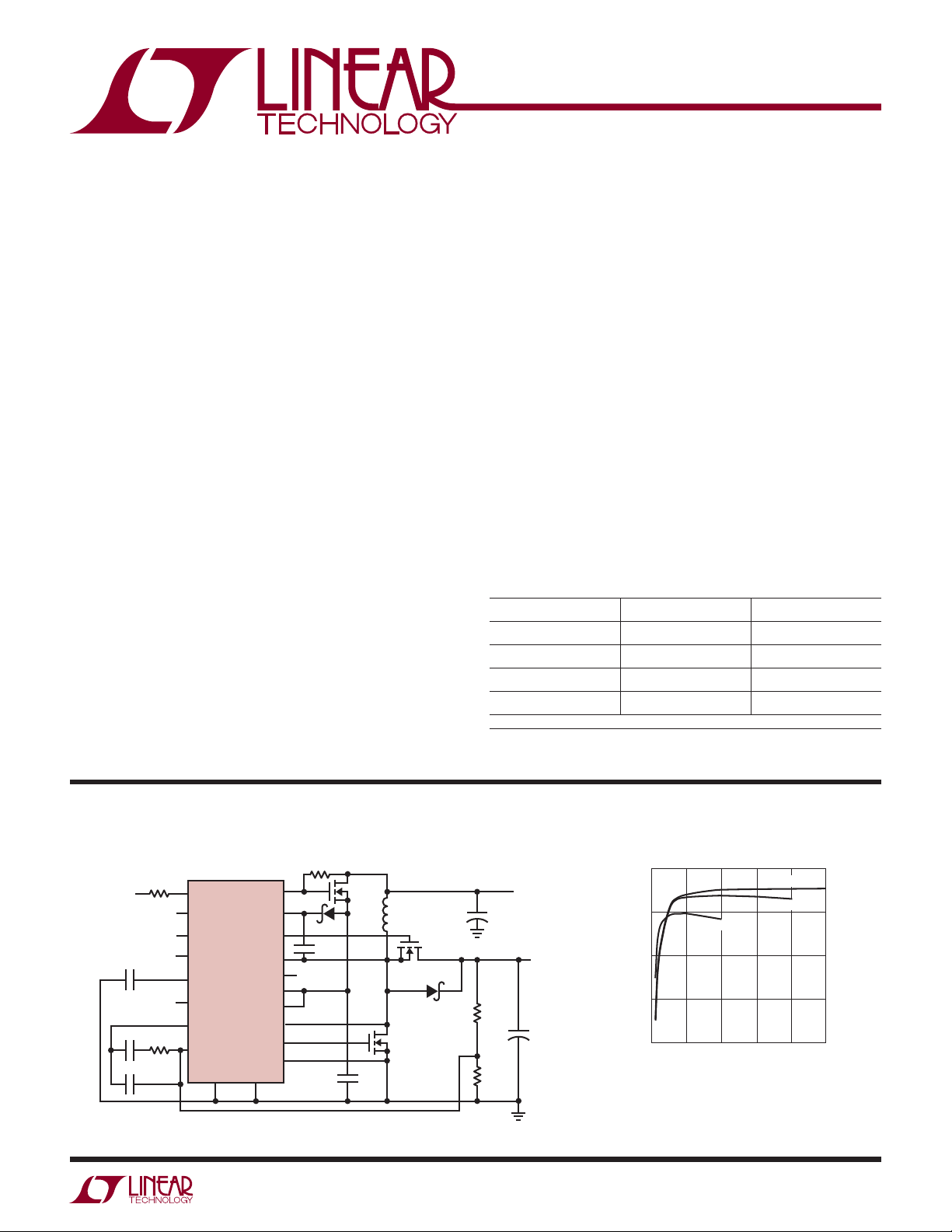
TYPICAL APPLICATION
High Effi ciency High Voltage Step-Up Converter
500k
V
OUT
1000pF
0.01
100pF
I
OFF
PGOOD
V
RNG
SYNC
SS
SHDN
I
100k
TH
V
FB
SGND
μ
F
LTC3813
BOOST
EXTV
DRV
INTV
SENSE
SENSE
BGRTN
NDRV
TG
SW
CC
CC
CC
+
BG
–
50k
0.1μF
Effi ciency vs Load Current
100
V
IN
22
30.9k
499
μ
Ω
3813 TA01
10V TO 40V
F
+
V
OUT
50V/5A
270μF
× 2
95
90
EFFICIENCY (%)
85
80
04
VIN = 12V
123 5
LOAD (A)
M1
Si7850DP
+
10
μ
H
D1
MBR1100
M2
Si7850DP
× 2
1
μ
F
VIN = 36V
VIN = 24V
3813 TA01b
3813fa
1
LTC3813
ABSOLUTE MAXIMUM RATINGS
(Note 1)
Supply Voltages
INTV
(DRV
BOOST ................................................ –0.3V to 114V
BGRTN ....................................................... –5V to 0V
EXTV
(NDRV - INTV
SW, SENSE
I
OFF
SS Voltage ................................................... –0.3V to 5V
PGOOD Voltage ............................................ –0.3V to 7V
V
RNG
UVIN Voltages ........................................ –0.3V to 14V
PLL/LPF, FB Voltages ................................. –0.3V to 2.7V
TG, BG, INTV
Operating Temperature Range (Note 2).... –40°C to 85°C
Junction Temperature (Notes 3, 7)........................ 125°C
Storage Temperature Range ................... –65°C to 150°C
Lead Temperature (Soldering, 10 sec) ..................300°C
, DRVCC ...................................... –0.3V to 14V
CC
- BGRTN), (BOOST - SW) ......... –0.3V to 14V
CC
.................................................. –0.3V to 15V
CC
) Voltage ........................... –0.3V to 10V
CC
+
Voltage ................................... –1V to 100V
Voltage .............................................. –0.3V to 100V
, V
, SYNC, SHDN,
OFF
, EXTVCC RMS Currents .................50mA
CC
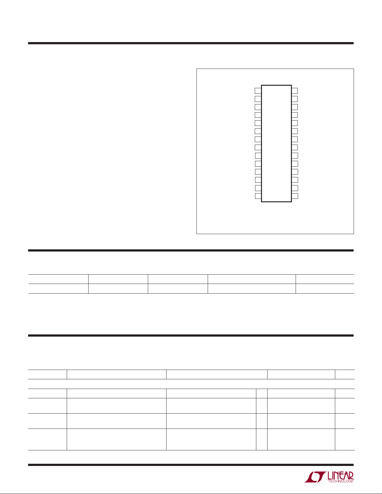
PIN CONFIGURATION
TOP VIEW
I
1
OFF
NC
2
NC
3
V
4
OFF
V
5
RNG
PGOOD
6
SYNC
7
I
8
TH
V
9
FB
PLL/LPF
10
SS
11
SGND
12
SHDN
13
UVIN
14
G PACKAGE
28-LEAD PLASTIC SSOP
T
= 125°C, θJA = 100°C/W
JMAX
28
27
26
25
24
23
22
21
20
19
18
17
16
15
BOOST
TG
SW
SENSE
NC
NC
NC
SENSE
BGRTN
BG
DRV
CC
INTV
EXTV
NDRV
+
–
CC
CC
ORDER INFORMATION
LEAD FREE FINISH TAPE AND REEL PART MARKING PACKAGE DESCRIPTION TEMPERATURE RANGE
LTC3813EG#PBF LTC3813EG#TRPBF LTC3813EG 28-Lead Plastic SSOP –40°C to 85°C
Consult LTC Marketing for parts specifi ed with wider operating temperature ranges.
Consult LTC Marketing for information on non-standard lead based fi nish parts.
For more information on lead free part marking, go to: http://www.linear.com/leadfree/
For more information on tape and reel specifi cations, go to: http://www.linear.com/tapeandreel/
The
ELECTRICAL CHARACTERISTICS
temperature range, otherwise specifi cations are at TA = 25°C, INTVCC = DRVCC = V
V
NDRV
= 10V, V
SYNC
= V
SENSE
+
= V
SYMBOL PARAMETER CONDITIONS MIN TYP MAX UNITS
Main Control Loop
INTV
I
Q
I
BOOST
V
FB
CC
INTVCC Supply Voltage
INTVCC Supply Current
INTV
Shutdown Current
CC
BOOST Supply Current (Note 5)
Feedback Voltage (Note 4)
SENSE
–
= V
= VSW = 0V, unless otherwise specifi ed.
BGRTN
l denotes specifi cations which apply over the full operating
= V
= V
= SHDN = UVIN = V
RNG
l
6.35 14 V
3
240
SHDN > 1.5V, I
SHDN = 0V
= 9.5V (Note 5)
NTVCC
BOOST
OFF
270
SHDN = 0V
0°C to 85°C
–40°C to 85°C
0.796
l
0.794
l
0.792
0
0.800
0.800
0.800
EXTVCC
6
600
400
5
0.804
0.806
0.806
=
mA
μA
μA
μA
V
V
V
2
3813fa
LTC3813
ELECTRICAL CHARACTERISTICS
The l denotes specifi cations which apply over the full operating
temperature range, otherwise specifi cations are at T
V
NDRV
= 10V, V
SYNC
= V
SENSE
+
= V
SENSE
–
= V
BGRTN
= 25°C, INTVCC = DRVCC = V
A
= V
= 0V, unless otherwise specifi ed.
SW
SYMBOL PARAMETER CONDITIONS MIN TYP MAX UNITS
ΔV
FB,LINE
V
SENSE(MAX)
V
SENSE(MIN)
I
VFB
(EA) Error Amplifi er DC Open Loop Gain 65 100 dB
A
VOL
f
U
I
SYNC
V
SHDN
I
SHDN
I
SS
V
VINUV
Feedback Voltage Line Regulation 7V < INTVCC < 14V (Note 4)
Maximum Current Sense Threshold V
Minimum Current Sense Threshold V
= 2V, VFB = 0.76V
RNG
V
= 0V, VFB = 0.76V
RNG
V
= INTVCC, VFB = 0.76V
RNG
= 2V, VFB = 0.84V
RNG
V
= 0V, VFB = 0.84V
RNG
V
= INTVCC, VFB = 0.84V
RNG
Feedback Current VFB = 0.8V 20 150 nA
Error Amp Unity Gain Crossover Frequency (Note 6) 25 MHz
SYNC Current 01 μA
Shutdown Threshold 1.2 1.5 2 V
SHDN Pin Input Current 01 μA
SS Source Current VSS > 0.5V 0.7 1.4 2.5 μA
VIN Undervoltage Lockout VIN Rising
V
Falling
IN
Hysteresis
V
VCCUV
INTVCC Undervoltage Lockout INTVCC Rising
Hysteresis
Oscillator and Phase-Locked Loop
t
OFF
t
OFF(MIN)
t
ON(MIN)
t
OFF(PLL)
I
PLL/LPF
Off-Time I
Minimum Off-Time I
Minimum On-Time 250 ns
t
Modulation Range by PLL
OFF
Down Modulation
Up Modulation
Phase Detector Output Current
Sinking Capability
Sourcing Capability
= 100μA
OFF
I
= 300μA
OFF
= 2000μA 100 ns
OFF
I
= 100μA, V
OFF
I
= 100μA, V
OFF
f
< f
PLLIN
f
> f
PLLIN
SW
SW
PLL/LPF
PLL/LPF
= 0.6V
= 1.8V
Driver
I
BG,PEAK
R
BG,SINK
I
TG,PEAK
R
TG,SINK
BG Driver Peak Source Current VBG = 0V 1.5 2 A
BG Driver Pulldown R
DS(ON)
TG Driver Peak Source Current VTG – VSW = 0V 1.5 2 A
TG Driver Pulldown R
DS(ON)
PGOOD Output
ΔV
FBOV
PGOOD Upper Threshold
PGOOD Lower Threshold
ΔV
FB,HYST
V
PGOOD
I
PGOOD
PGOOD Hysteresis VFB Returning 1.5 3 %
PGOOD Low Voltage I
PGOOD Leakage Current V
PG Delay PGOOD Delay V
VFB Rising
V
Falling
FB
= 5mA 0.3 0.6 V
PGOOD
= 5V 0 2 μA
PGOOD
Falling 125 μs
FB
BOOST
= V
OFF
= V
= SHDN = UVIN = V
RNG
l
256
70
170
l
0.86
l
0.78
0.07
l
6.05 6.2
1.55
515
2.2
0.6
7.5
–7.5
=
EXTVCC
0.002 0.02 %/V
320
95
215
–300
–85
–200
0.88
0.80
0.10
384
120
260
0.92
0.82
0.12
mV
mV
mV
mV
mV
mV
6.35 V
0.2
1.85
605
3.6
1.2
15
–25
2.15
695
5
1.8
μA
μA
11.5
11.5
10
–10
12.5
–12.5
V
V
V
V
μs
ns
μs
μs
Ω
Ω
%
%
3813fa
3
LTC3813
ELECTRICAL CHARACTERISTICS
The l denotes specifi cations which apply over the full operating
temperature range, otherwise specifi cations are at T
V
NDRV
= 10V, V
SYNC
= V
SENSE
+
= V
SENSE
–
= V
BGRTN
= 25°C, INTVCC = DRVCC = V
A
= V
= 0V, unless otherwise specifi ed.
SW
SYMBOL PARAMETER CONDITIONS MIN TYP MAX UNITS
Regulators
V
CC
V
EXTVCC
V
INTVCC,1
ΔV
EXTVCC,1
ΔV
LOADREG,1
V
INTVCC,2
ΔV
LOADREG,2
I
NDRV
V
CCSR
I
CCSR
EXTVCC Switchover Voltage
EXTV
Rising
CC
EXTV
Hysteresis
CC
INTVCC Voltage from EXTV
V
EXTVCC
- V
at Dropout ICC = 20mA, V
INTVCC
CC
INTVCC Load Regulation from EXTV
CC
10.5V < V
I
CC
EXTVCC
= 0mA to 20mA, V
< 15V 9.4 10 10.6 V
= 9.1V 170 250 mV
EXTVCC
EXTVCC
INTVCC Voltage from NDRV Regulator Linear Regulator in Operation 9.4 10 10.6 V
INTVCC Load Regulation from NDRV ICC = 0mA to 20mA, V
Current into NDRV Pin V
NDRV
– V
INTVCC
EXTVCC
= 3V 20 40 60 μA
Maximum Supply Voltage Trickle Charger Shunt Regulator 15 V
Maximum Current into NDRV/INTV
CC
Trickle Charger Shunt Regulator,
INTV
≤ 16.7V (Note 8)
CC
= V
= V
BOOST
OFF
= SHDN = UVIN = V
RNG
l
6.4
0.1
6.7
0.25 0.5
EXTVCC
=
= 12V 0.01 %
= 0 0.01 %
10 mA
V
V
Note 1: Stresses beyond those listed under Absolute Maximum Ratings
may cause permanent damage to the device. Exposure to any Absolute
Maximum Rating condition for extended periods may affect device
reliability and lifetime.
Note 2: The LTC3813E is guaranteed to meet performance specifi cations
from 0°C to 85°C. Specifi cations over the –40°C to 85°C operating
temperature range are assured by design, characterization and correlation
with statistical process controls.
Note 3: T
dissipation P
LTC3813: T
Note 4: The LTC3813 is tested in a feedback loop that servos V
reference voltage with the I
is calculated from the ambient temperature TA and power
J
according to the following formula:
D
= TA + (PD • 100°C/W)
J
pin forced to a voltage between 1V and 2V.
TH
FB
to the
Note 5: The dynamic input supply current is higher due to the power
MOSFET gate charging being delivered at the switching frequency
(Q
• fSW).
G
Note 6: Guaranteed by design. Not subject to test.
Note 7: This IC includes overtemperature protection that is intended
to protect the device during momentary overload conditions. Junction
temperature will exceed 125°C when overtemperature protection is active.
Continuous operation above the specifi ed maximum operating junction
temperature may impair device reliability.
Note 8: I
is the sum of current into NDRV and INTVCC.
CC
4
3813fa
LTC3813
TYPICAL PERFORMANCE CHARACTERISTICS
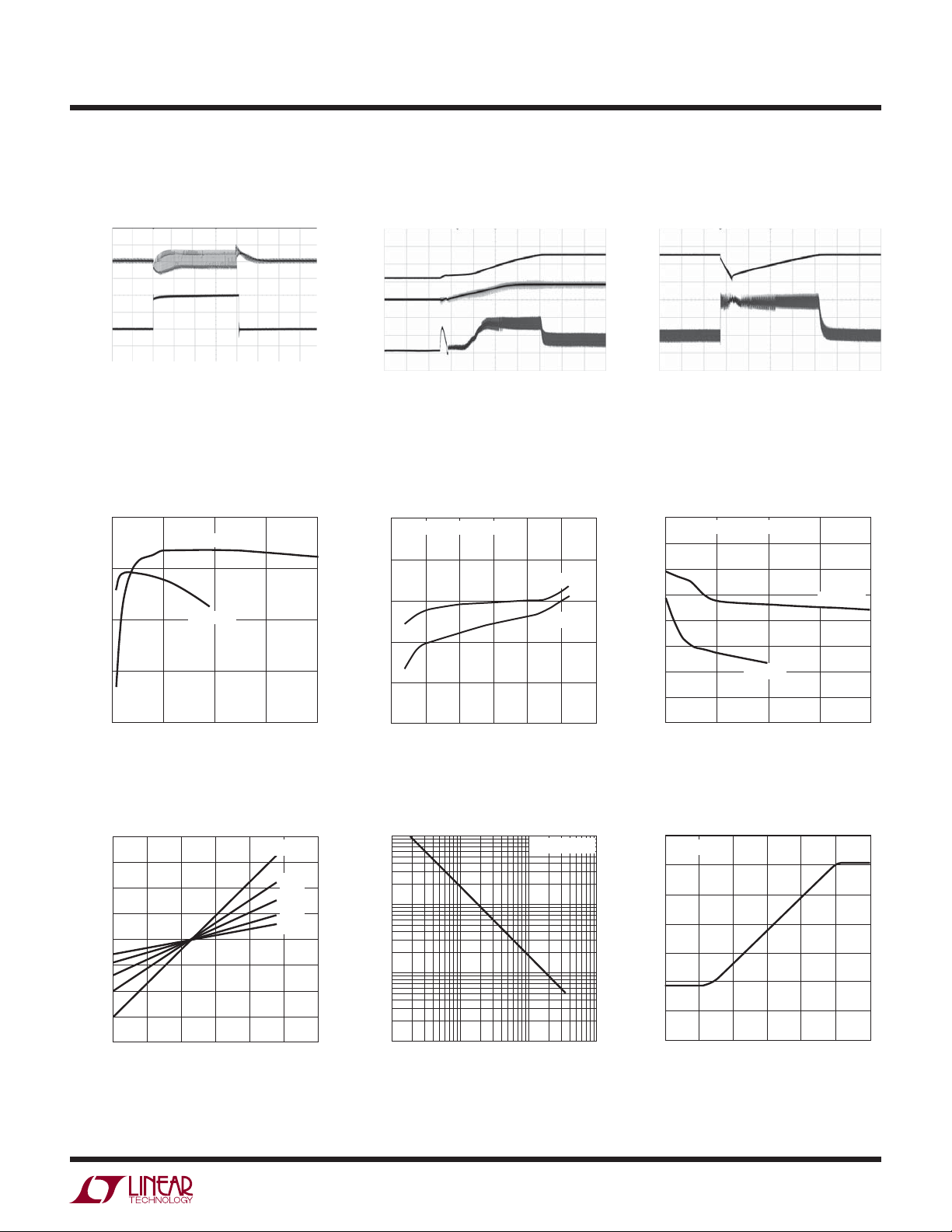
Load Transient Response Start-Up
V
OUT
200mV/
DIV
I
OUT
2A/DIV
FIGURE 14 CIRCUIT
= 12V
V
IN
0A TO 4A LOAD STEP
Effi ciency vs Load Current
100
V
= 24V
OUT
95
90
EFFICIENCY (%)
85
80
0
1
100μs/DIV
VIN = 12V
VIN = 5V
2
LOAD (A)
3813 G01
3
3813 G04
4
V
OUT
20V/DIV
SS
4V/DIV
I
L
5A/DIV
FRONT PAGE CIRCUIT
= 24V
V
IN
= 2A
I
LOAD
Frequency vs Input Voltage
300
FRONT PAGE CIRCUIT
280
260
240
FREQUENCY (kHz)
220
200
15
10
INPUT VOLTAGE (V)
20
1ms/DIV
25
I
LOAD
I
LOAD
30 35
= 0A
= 1A
3813 G02
3813 G05
40
Overcurrent Operation
V
OUT
20V/DIV
I
L
5A/DIV
FRONT PAGE CIRCUIT
= 24V
V
IN
= 1Ω
R
SHORT
Frequency vs Load Current
280
FRONT PAGE CIRCUIT
270
260
250
240
230
FREQUENCY (kHz)
220
210
200
0
1
LOAD CURRENT (A)
500μs/DIV
VIN = 12V
2
VIN = 24V
3
3813 G03
4
3813 G06
Current Sense Threshold
Voltage
vs I
TH
400
300
200
100
0
–100
–200
CURRENT SENSE THRESHOLD (mV)
–300
–400
0
0.5
1 1.5 2
ITH VOLTAGE (V)
V
RNG
1.4V
1V
0.7V
0.5V
2.5 3
= 2V
3813 G07
Off-Time vs I
10000
1000
OFF-TIME (ns)
100
10
10
Current
OFF
V
= INTV
OFF
CC
100 1000 10000
I
CURRENT (μA)
OFF
3813 G08
Off-Time vs V
700
I
OFF
600
500
400
300
OFF-TIME (ns)
200
100
0
0
= 300μA
0.5 1
Voltage
OFF
1.5 2.5
V
VOLTAGE (V)
OFF
23
3813 G09
3813fa
5
LTC3813
TYPICAL PERFORMANCE CHARACTERISTICS
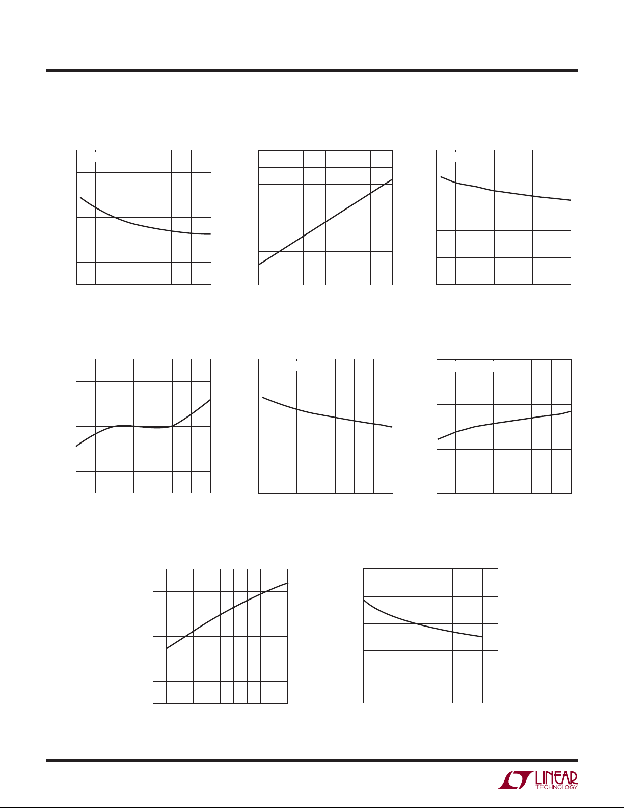
Off-Time vs Temperature
680
I
= 300μA
OFF
660
640
620
OFF-TIME (ns)
600
580
560
–50
–25 0
25 75
TEMPERATURE (°C)
Feedback Reference Voltage
vs Temperature
0.803
0.802
0.801
0.800
0.799
REFERENCE VOLTAGE (V)
0.798
50 100 125
3813 G10
Maximum Current Sense
Threshold vs V
400
300
200
100
MAXIMUM CURRENT SENSE THRESHOLD (mV)
0
0.5
V
Voltage
RNG
1 1.5
VOLTAGE (V)
RNG
Driver Peak Source Current
vs Temperature
2.5
V
= V
INTVCC
= 10V
BOOST
2.0
1.5
PEAK SOURCE CURRENT (A)
3813 G11
Maximum Current Sense
Threshold vs Temperature
230
V
= INTV
RNG
220
210
200
190
MAXIMUM CURRENT SENSE THRESHOLD (mV)
180
2
–50 –25
CC
25
0
TEMPERATURE (°C)
Driver Pulldown R
vs Temperature
1.50
V
= V
INTVCC
= 10V
1.25
1.00
(Ω)
0.75
DS(ON)
R
0.50
0.25
BOOST
50
DS(ON)
100
125
3813 G12
75
6
0.797
–50 –25
50
25
0
TEMPERATURE (°C)
Driver Peak Source Current
vs Supply Voltage
3.0
2.5
2.0
1.5
1.0
PEAK SOURCE CURRENT (A)
0.5
0
56 8 10 12 14
75
125
100
3813 G13
7 9 11 13
DRVCC/BOOST VOLTAGE (V)
1
–25 0 25 50
–50
15
3813 G16
TEMPERATURE (°C)
(Ω)
R
75 100 125
3813 G14
Driver Pulldown R
vs Supply Voltage
1.1
1.0
0.9
DS(ON)
0.8
0.7
0.6
79
8
6
DRVCC/BOOST VOLTAGE (V)
0
–50
–25 0
DS(ON)
11 15
12
10
25 75
TEMPERATURE (°C)
13
14
3813 G17
50 100 125
3813 G15
3813fa
TYPICAL PERFORMANCE CHARACTERISTICS
LTC3813
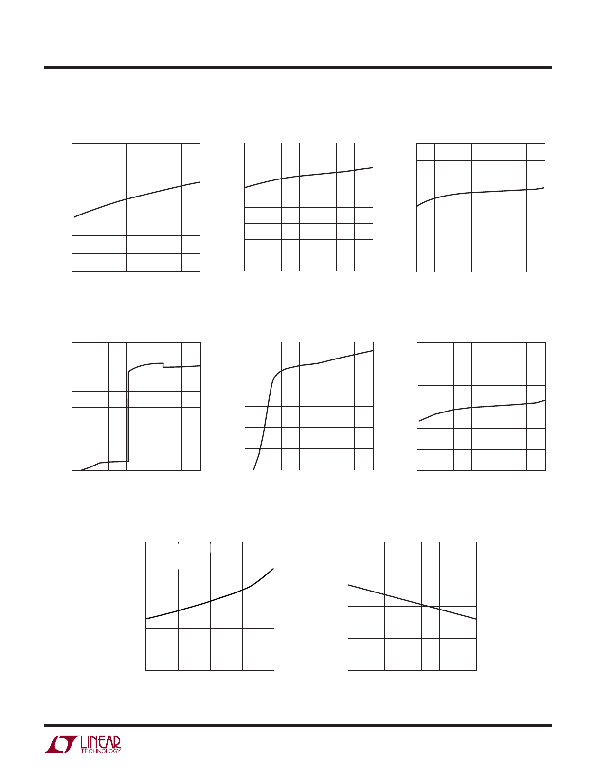
EXTVCC LDO Resistance at
Dropout vs Temperature
14
12
10
8
6
RESISTANCE (Ω)
4
2
0
–25 0 50
–50
25
TEMPERATURE (°C)
INTVCC Current vs INTVCC Voltage
4.0
3.5
3.0
2.5
2.0
CURRENT (mA)
1.5
CC
INTV
1.0
0.5
0
0
24
INTVCC VOLTAGE (V)
81214
610
75 100 125
3813 G18
3813 G21
INTV
Current vs Temperature
CC
4
3
2
CURRENT (mA)
CC
INTV
1
0
–50 –25
25
0
TEMPERATURE (°C)
INTVCC Shutdown Current
vs INTVCC Voltage
300
250
200
150
CURRENT (μA)
CC
100
INTV
50
0
0
24
610
INTVCC VOLTAGE (V)
50
75
81214
100
125
3813 G19
3813 G22
Shutdown Current
INTV
CC
vs Temperature
400
300
200
CURRENT (μA)
CC
INTV
100
0
–25 0 50
–50
SS Pull-Up Current
vs Temperature
3
2
1
SS CURRENT (μA)
0
–50
–25 0
25
TEMPERATURE (°C)
50 100 125
25 75
TEMPERATURE (°C)
75 100 125
3813 G20
3813 G23
ITH Voltage
vs Load Current
3
FRONT PAGE CIRCUIT
= 24V
V
IN
V
RNG
2
VOLTAGE (V)
TH
I
1
0
0
= 1V
1234
LOAD CURRENT (A)
3813 G24
Shutdown Threshold
vs Temperature
2.2
2.0
1.8
1.6
1.4
1.2
1.0
SHUTDOWN THRESHOLD (V)
0.8
0.6
–25 0 50
–50
25
TEMPERATURE (°C)
75 100 125
3813 G25
3813fa
7

LTC3813
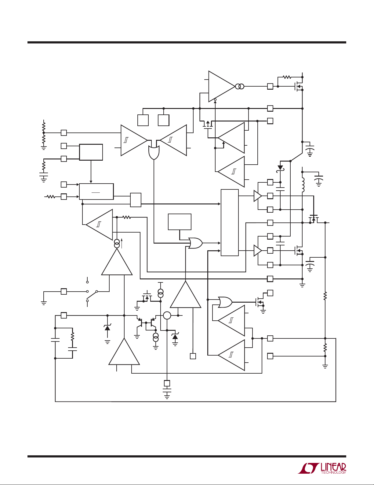
PIN FUNCTIONS
I
(Pin 1): Off-Time Current Input. Tie a resistor from
OFF
to this pin to set the one-shot timer current and
V
OUT
thereby set the switching frequency.
(Pin 4): Off-Time Voltage Input. Voltage trip point
V
OFF
for the on-time comparator. Tying this pin to an external
resistive divider from the input makes the off-time proportional to V
the pin is grounded and defaults to 2.4V when the pin is
connected to INTV
(Pin 5): Sense Voltage Limit Set. The voltage at this
V
RNG
pin sets the nominal sense voltage at maximum output
current and can be set from 0.5V to 2V by a resistive
divider from INTV
to 95mV when this pin is tied to ground, and 215mV when
tied to INTV
PGOOD (Pin 6): Power Good Output. Open-drain logic
output that is pulled to ground when the output voltage
is not between ±10% of the regulation point. The output
voltage must be out of regulation for at least 125μs before
the power good output is pulled to ground.
SYNC (Pin 7): Sync Pin. This pin provides an external
clock input to the phase detector. The phase-locked loop
will force the rising top gate signal to be synchronized
with the rising edge of the clock signal.
(Pin 8): Error Amplifi er Compensation Point and Cur-
I
TH
rent Control Threshold. The current comparator threshold
increases with control voltage. The voltage ranges from
0V to 2.6V with 1.2V corresponding to zero sense voltage
(zero current).
(Pin 9): Feedback Input. Connect VFB through a resistor
V
FB
divider network to V
PLL/LPF (Pin 10): The phase-locked loop’s lowpass fi lter
is tied to this pin. The voltage at this pin defaults to 1.2V
when the IC is not synchronized with an external clock at
the SYNC pin.
. The comparator defaults to 0.7V when
IN
.
CC
. The nominal sense voltage defaults
CC
.
CC
to set the output voltage.
OUT
SS (Pin 11): Soft-Start Input. A capacitor to ground at
this pin sets the ramp rate of the maximum current sense
threshold.
SGND (Pin 12): Signal Ground. All small signal components
should connect to this ground and eventually connect to
PGND at one point.
SHDN (Pin 13): Shutdown Pin. Pulling this pin below 1.5V
will shut down the LTC3813, turn off both of the external
MOSFET switches and reduce the quiescent supply current to 240μA.
UVIN (Pin 14): UVLO Input. This pin is input to the internal
UVLO and is compared to an internal 0.8V reference. An
external resistor divider is connected to this pin and the
input supply to program the undervoltage lockout voltage.
When UVIN is less than 0.8V, the LTC3813 is shut down.
NDRV (Pin 15): Drive Output for External Pass Device of
the Linear Regulator for INTV
. Connect to the gate of an
CC
external NMOS pass device and a pull-up resistor to the
input voltage V
EXTV
(Pin 16): External Driver Supply Voltage. When
CC
or the output voltage V
IN
OUT
.
this voltage exceeds 6.7V, an internal switch connects
this pin to INTV
through an LDO and turns off the exter-
CC
nal MOSFET connected to NDRV, so that controller and
gate drive are drawn from EXTV
INTV
(Pin 17): Main Supply Pin. All internal circuits
CC
CC
.
except the output drivers are powered from this pin.
INTV
should be bypassed to ground (Pin 10) with at
CC
least a 0.1μF capacitor in close proximity to the
LTC3813.
(Pin 18): Driver Supply Pin. DRVCC supplies power
DRV
CC
to the BG output driver. This pin is normally connected to
INTV
. DRVCC should be bypassed to BGRTN (Pin 20)
CC
with a low ESR (X5R or better) 1μF capacitor in close
proximity to the LTC3813.
8
3813fa

PIN FUNCTIONS
LTC3813
BG (Pin 19): Bottom Gate Drive. The BG pin drives the
gate of the bottom N-channel main switch MOSFET. This
pin swings from BGRTN to DRV
BGRTN (Pin 20): Bottom Gate Return. This pin connects to
the source of the pulldown MOSFET in the BG driver and
is normally connected to ground. Connecting a negative
supply to this pin allows the main MOSFET’s gate to be
pulled below ground to help prevent false turn-on during
high dV/dt transitions on the SW node. See the Applications Information section for more details.
+
SENSE
parator Input. The (+) input to the current comparator is
normally connected to SW unless using a sense resistor.
The (–) input is used to accurately kelvin sense the bottom
side of the sense resistor or MOSFET.
, SENSE– (Pin 25, Pin 21): Current Sense Com-
CC
.
SW (Pin 26): Switch Node Connection to Inductor and
Bootstrap Capacitor. Voltage swing at this pin is from a
Schottky diode (external) voltage drop below ground
to V
TG (Pin 27): Top Gate Drive. The TG pin drives the gate of
the top N-channel synchronous switch MOSFET. The TG
driver draws power from the BOOST pin and returns to the
SW pin, providing true fl oating drive to the top MOSFET.
BOOST (Pin 28): Top Gate Driver Supply. The BOOST pin
supplies power to the fl oating TG driver. BOOST should
be bypassed to SW with a low ESR (X5R or better) 0.1μF
capacitor. An additional fast recovery Schottky diode from
DRV
charge-pumped supply at BOOST.
.
OUT
to the BOOST pin will create a complete fl oating
CC
3813fa
9
LTC3813
FUNCTIONAL DIAGRAM
V
IN
R
UVIN
UV1
14
R
UV2
SYNC
7
R
C
C
PLL-SYNC
t
= (76pF)
OFF
1.4V
0.7V
C1
V
VOFF
I
IOFF
I
CMP
PLL/LPF
10
V
OFF
4
I
OFF
R
OFF
V
OUT
1
V
RNG
5
I
TH
8
C
C2
0.8V
–
+
20k
+
–
×
2.6V
EA
+
VINUV
R
SQ
–
5V
REG
FAULT
0.8V
REF
1.4μA
Σ
+
INTV
CC
UV
OVERTEMP
SENSE
RUN
SHDN
+
–
1.5V
4V
V
IN
10V
+
NDRV
15
M3
–
OFF
–
6.2V
+
ON
+
–
+
–
ON
SWITCH
LOGIC
SHDN
OV
10V
6.7V
INTV
17
EXTV
16
BOOST
28
TG
27
SW
26
SENSE
25
DRV
18
BG
19
BGRTN
20
SENSE
21
PGOOD
6
CC
CC
+
V
D
B
+
CC
–
IN
+
C
IN
M2
L
V
M1
+
OUT
C
OUT
R2
C
B
C
VCC
–
0.72V
+
UV
13
SHDN
–
+
OV
–
0.85V
V
FB
9
SGND
12
R1
10
0.8V
SS
11
3813 FD
3813fa
 Loading...