

查询LTC3806供应商
FEATURES
■
High Efficiency at Full Load
■
Better Cross Regulation Than Nonsynchronous
Converters (Multiple Outputs)
■
Soft-Start Minimizes Inrush Current
■
Current Mode Control Provides Excellent
Transient Response
■
High Maximum Duty Cycle: 89% Typical
■
±2% Programmable Undervoltage Lockout Threshold
■
±1% Internal Voltage Reference
■
Micropower Start-Up
■
Constant Frequency Operation (Never Audible)
■
3mm × 4mm 12-Pin DFN Package
LTC3806
Synchronous
Flyback DC/DC Controller
U
DESCRIPTIO
The LTC®3806 is a current mode synchronous flyback
controller that drives N-channel power MOSFETs and
requires very few external components. It is intended for
medium power applications where multiple outputs are
required. Synchronous rectification provides higher efficiency and improved output cross regulation than
nonsynchronous converters.
The IC contains all the necessary control circuitry including a 250kHz oscillator, precision undervoltage lockout
circuit with hysteresis, gate drivers for primary and synchronous switches, current mode control circuitry and
soft-start circuitry.
U
APPLICATIO S
■
48V Telecom Supplies
■
12V/42V Automotive
■
24V Industrial
■
VoIP Phone
■
Power Over Ethernet
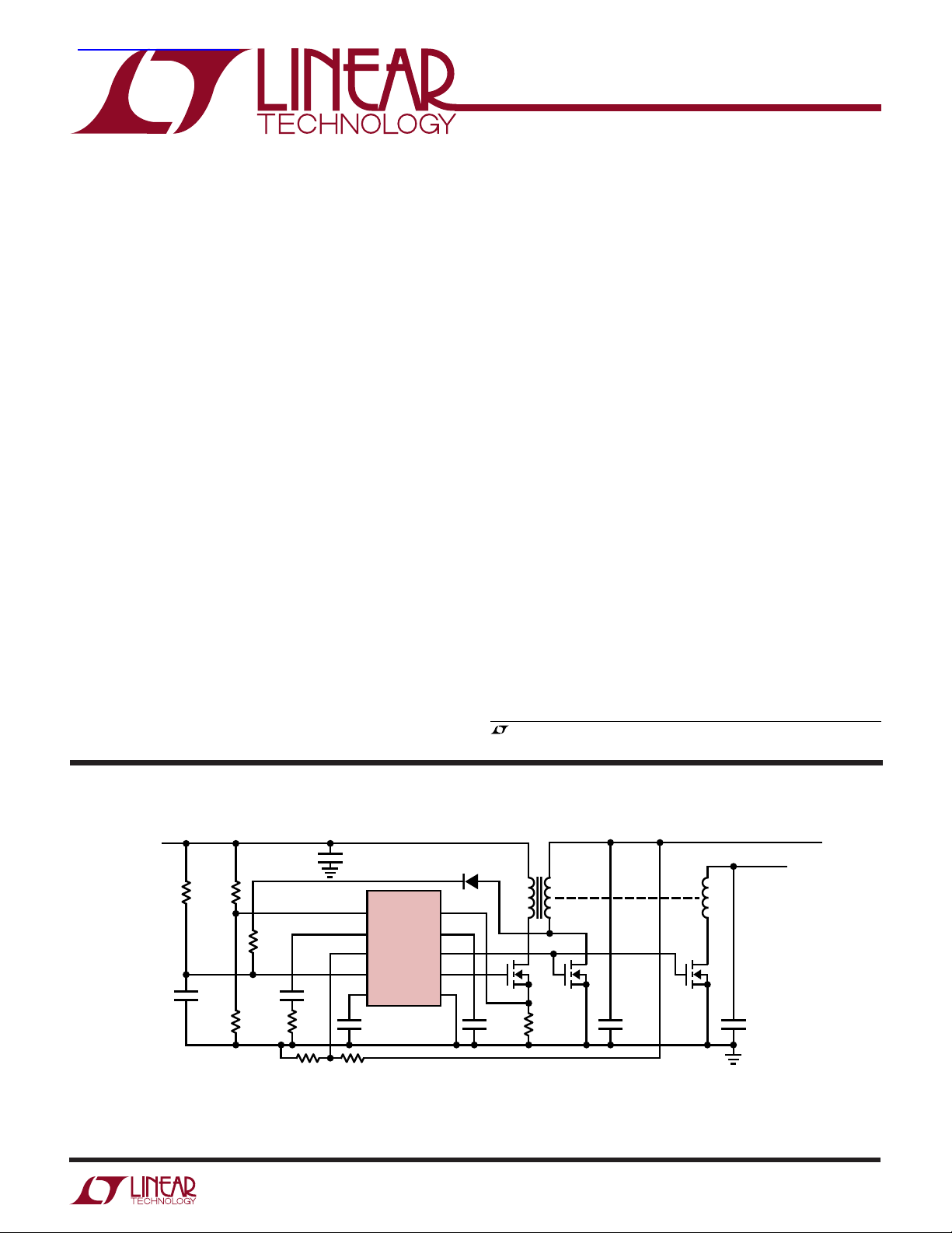
TYPICAL APPLICATIO
V
IN
36V TO 72V
604k
C1
100µF
R2
R8
100Ω
R3
26.7k
51k
R1
R4
3.4k
C2
1nF
U
C7
4.7µF
RUN
I
TH
FB
V
IN
INTV
C3
4.7µF
LTC3806
SENSE
CC
GND
Programmable soft-start reduces inrush currents. This
makes it easier to design compliant Power Over Ethernet
supplies.
Low start-up current reduces power dissipation in the
start-up resistor and reduces the size of the external startup capacitor.
The LTC3806 is available in a 12-pin, exposed pad DFN
package.
, LTC and LT are registered trademarks of Linear Technology Corporation.
V
OUT1
3.3V
V
3A
C6
470µF
OUT2
2.5V
3A
D1
SS
G2
G1
T1
•
••
M1 M2 M3
C4
0.47µF
R5
0.056Ω
C5
470µF
R7
12.4k
R6
21k
Figure 1. Multiple Output Flyback Converter for Telecom
3806 F01
3806f
1
LTC3806
12
11
10
9
8
7
1
2
3
4
5
6
SENSE
NC
SS
G1
G2
GND
RUN
I
TH
FB
NC
V
IN
INTV
CC
TOP VIEW
13
DE12 PACKAGE
12-LEAD (4mm × 3mm) PLASTIC DFN
ABSOLUTE MAXIMUM RATINGS
(Note 1)
VIN Voltage ............................................................. 25V
INTVCC Voltage ......................................................... 8V
INTVCC Output Current ........................................ 50mA
G1, G2 Voltages....................... –0.3V to V
ITH, FB, SS Voltages .................................–0.3V to 2.7V
RUN Voltage ............................................... –0.3V to 7V
SENSE Pin Voltage ..................................... –0.3V to 8V
Operating Ambient Temperature Range
(Note 2) .................................................. – 40°C to 85°C
Junction Temperature (Note 3)............................ 125°C
Storage Temperature Range ................. –65°C to 125°C
ELECTRICAL CHARACTERISTICS
temperature range, otherwise specifications are TA = 25°C. VIN = 10V, V
SYMBOL PARAMETER CONDITIONS MIN TYP MAX UNITS
Main Control Loop
V
IN(MIN)
I
Q
+
V
RUN
–
V
RUN
V
RUN(HYST)
I
RUN
V
FB
I
FB
∆VFB/∆VINLine Regulation 10V ≤ VIN ≤ 20V 0.01 %/V
∆VFB/∆V
g
m
V
SENSE(MAX)
I
SENSE(ON)
I
SENSE(OFF)
I
SS
Oscillator
f
OSC
DC(MAX) Maximum Duty Cycle 84 89 94 %
2
Minimum Input Voltage (Note 4) 10 V
Input Voltage Supply Current (Note 5)
Quiescent 1000 µA
Shutdown Mode V
Start-Up Mode V
Rising RUN Input Threshold Voltage VIN = 20V 1.205 1.230 1.255 V
Falling RUN Input Threshold Voltage VIN = 20V 1.116 1.139 1.162 V
RUN Pin Input Threshold Hysteresis VIN = 20V 45 91 137 mV
RUN Input Current 160 nA
Feedback Voltage V
Feedback Pin Input Current V
Load Regulation VTH = 0.55V to 0.95V (Note 6) ● –1 –0.1 %
ITH
Error Amplifier Transconductance ITH Pin Load = ±5µA (Note 6) 650 µMho
Maximum Current Sense Input Threshold 110 150 190 mV
SENSE Pin Current (G1 High) V
SENSE Pin Current (G1 Low) V
SS Pin Source Current VSS = 1.5V 3 5 8 µA
Oscillator Frequency 210 250 290 kHz
WW
W
U
INTVCC
+ 0.3V
The ● denotes specifications which apply over the full operating
= 0V 50 90 µA
RUN
> 1.255V, VIN < 7V 80 140 µA
RUN
= 0.75V (Note 6) 1.218 1.230 1.242 V
ITH
= 0.75V (Note 6) 18 100 nA
ITH
= 0V 35 50 µA
SENSE
= 1V 0.1 5 µA
SENSE
U
W
U
PACKAGE/ORDER INFORMATION
ORDER PART
NUMBER
LTC3806EDE
DE PART MARKING
3806
T
= 125°C, θJA = 34°C/W
JMAX
EXPOSED PAD (PIN 13) IS GND
MUST BE SOLDERED TO PCB
Consult LTC Marketing for parts specified with wider operating temperature ranges.
= 1.5V, unless otherwise specified.
RUN
● 1.181 1.279 V
● 1.093 1.185 V
● 1.212 1.248 V
3806f
LTC3806
TEMPERATURE (°C)
–40
0
FB PIN CURRENT (nA)
5
10
15
20
25
30
–15 10 35 60
3806 G03
85
ELECTRICAL CHARACTERISTICS
temperature range, otherwise specifications are TA = 25°C. VIN = 10V, V
The ● denotes specifications which apply over the full operating
= 1.5V, unless otherwise specified.
RUN
SYMBOL PARAMETER CONDITIONS MIN TYP MAX UNITS
Regulator
V
INTVCC
∆INTV
∆V
IN
V
LDO(LOAD)
+
V
UVL
–
V
UVL
INTVCC Regulator Output Voltage VIN = 10V 6 6.9 7.8 V
INTVCC Regulator Line Regulation 10V ≤ VIN ≤ 20V 100 mV
CC
INTVCC Load Regulation 0 ≤ I
≤ 20mA –6 –3 %
INTVCC
Rising VIN Threshold Voltage 14 15 16 V
Falling VIN Threshold Voltage 7.5 8 8.5 V
Gate Drivers
t
r1
t
f1
t
r2
t
f2
t
DEAD
Note 1: Absolute Maximum Ratings are those values beyond which the life
of the device may be impaired.
Note 2: The LTC3806E is guaranteed to meet performance specifications
from 0°C to 70°C. Specifications over the –40°C to 85°C operating
temperature range are assured by design, characterization and correlation
with statistical process controls.
Note 3: T
dissipation P
TJ = TA + (PD • 34°C/W)
Gate Driver 1 Output Rise Time CL1 = 3300pF 25 100 ns
Gate Driver 1 Output Fall Time CL1 = 3300pF 18 100 ns
Gate Driver 2 Output Rise Time CL2 = 4700pF 25 100 ns
Gate Driver 2 Output Fall Time CL2 = 4700pF 18 100 ns
Gate Driver Dead Time CL1 = 3300pF, CL2 = 4700pF 100 ns
Note 4: The minimum operating voltage is allowed once operation begins.
To begin operation, V
threshold with V
must be above the rising undervoltage lockout
IN
above the rising RUN input threshold.
RUN
Note 5: The dynamic input supply current is higher due to power MOSFET
• f
gate charging (Q
). See Applications Information.
G
OSC
Note 6: The LTC3806 is tested in a feedback loop which servos VFB to the
is calculated from the ambient temperature TA and power
J
according to the following formula:
D
reference voltage with the I
(the no load to full load operating voltage range for the I
pin forced to a voltage between 0V and 1.4V
TH
pin is 0.3V to
TH
1.23V).
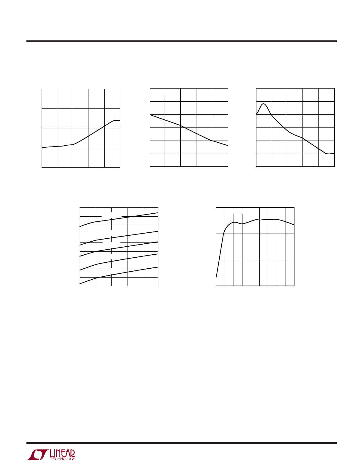
TYPICAL PERFOR A CE CHARACTERISTICS
1.2400
1.2350
1.2300
1.2250
FB VOLTAGE (V)
1.2200
1.2150
UW
FB Voltage vs Temperature FB Voltage Line Regulation FB Pin Current vs Temperature
1.2310
TA = 25°C
1.2305
1.2300
FB VOLTAGE (V)
1.2295
–40
–15
10
TEMPERATURE (°C)
35
60
3806 G01
1.2290
85
11
12
10
15
16
17
18
19
13
14
VIN (V)
20
3806 G02
3806f
3
LTC3806
TEMPERATURE (°C)
–40
1.10
RUN THRESHOLDS (V)
1.12
1.14
1.16
1.18
1.20
1.22
TRIP
–15 10 35 60
3806 G10
85
RELEASE
UW
TYPICAL PERFOR A CE CHARACTERISTICS
Shutdown Mode IQ vs V
80
TA = 25°C
70
60
(µA)
Q
50
40
30
20
SHUTDOWN MODE, I
10
0
4 8 12 20142 6 10 18
0
VIN (V)
G1 Rise and Fall Time vs C
250
TA = 25°C
200
150
TIME (ns)
100
Shutdown Mode I
IN
16
3806 G04
L
vs Temperature Soft-Start Current vs Temperature
80
75
(µA)
Q
70
65
60
SHUTDOWN MODE, I
55
50
–40
–15 10 35 60
G2 Rise and Fall Time vs C
120
TA = 25°C
100
80
60
TIME (ns)
40
Q
TEMPERATURE (°C)
7.0
6.5
6.0
5.5
SOFT-START CURRENT (µA)
85
3806 G05
L
5.0
–40
–15 10 35 60
TEMPERATURE (°C)
RUN Thresholds vs Temperature
85
3806 G06
50
0
20
4000
0
8000
CL (pF)
12000
16000
20000
3806 G07
0
4000
0
8000
12000
16000
20000
C
(pF)
L
3806 G08
Maximum Sense Threshold
Frequency vs Temperature
260
255
250
FREQUENCY (kHz)
245
240
–40
–15
10
TEMPERATURE (°C)
35
60
85
3806 G11
vs Temperature
155
154
153
152
151
150
149
148
147
MAX SENSE THRESHOLD (mV)
146
145
–40
–15
10
TEMPERATURE (°C)
35
60
85
3806 G12
3806f
4
UW
VIN (V)
10
6.990
INTV
CC
VOLTAGE (V)
6.995
7.000
7.005
7.010
7.015
7.020
12 14 16 18
3806 G15
20
TYPICAL PERFOR A CE CHARACTERISTICS
SENSE Pin Current
vs Temperature INTVCC Load Regulation INTVCC Line Regulation
32.0
31.5
7.020
7.015
7.010
TA = 25°C
LTC3806
SENSE PIN CURRENT (µA)
31.0
30.5
30.0
–40
–15
10
TEMPERATURE (°C)
2.8
2.7
2.6
2.5
2.4
2.3
2.2
DROPOUT VOLTAGE (V)
2.1
2.0
1.9
35
60
85
3806 G13
INTVCC Dropout Voltage
vs Current, Temperature
TA = –40°C
TA = 0°C
TA = 25°C
TA = 55°C
TA = 85°C
0
10 30
20
INTVCC LOAD (mA)
7.005
VOLTAGE (V)
CC
7.000
INTV
6.995
6.990
0
40
3806 G16
10 20 30 40
INTVCC LOAD (mA)
50
50
3806 G14
Efficiency vs Output Power
90
FIGURE 8 CIRCUIT
85
EFFICIENCY (%)
80
75
30 50 70 90
% OF MAXIMUM OUTPUT POWER
1002010 40 60 80
3806 G17
3806f
5

LTC3806
U
UU
PI FU CTIO S
RUN (Pin 1): The RUN pin provides the user with an
accurate means for sensing the input voltage and programming the start-up threshold for the converter. The
falling RUN pin threshold is nominally 1.14V and the
comparator has 91mV of hysteresis for noise immunity.
When the RUN pin is below this input threshold, the gate
drive outputs G1 and G2 are held low. The absolute
maximum rating for the voltage on this pin is 7V.
ITH (Pin 2): Error Amplifier Compensation Pin. The current
comparator input threshold increases with this control
voltage. Nominal voltage range for this pin is 0V to 1.4V.
FB (Pin 3): Receives the feedback voltage from the external resistor divider across the main output. Nominal
voltage for this pin in regulation is 1.230V.
NC (Pins 4, 11): Do Not Connect.
VIN (Pin 5): Main Supply Pin. Must be closely decoupled
to ground.
INTV
gate drivers and control circuits are powered from this
voltage. Decouple this pin locally to the IC ground with a
minimum 4.7µF low ESR ceramic capacitor.
GND (Pins 7, 13): Ground Pins. Exposed pad must be tied
to electrical ground.
G2 (Pin 8): Secondary-Side Gate Driver Output. This pin
drives the gates of all of the synchronous rectifiers.
G1 (Pin 9): Primary-Side Gate Driver Output.
SS (Pin 10): Soft-Start. A capacitor between this pin and
ground sets the rate at which the current comparator input
threshold may increase when the IC is initially enabled.
Increasing the size of the capacitor slows down the ramp
rate and reduces the inrush current.
SENSE (Pin 12): Current Sense Input for the Control Loop.
Connect this pin to the current sense resistor in the source
of the primary side power MOSFET. Internal leading edge
blanking is provided.
(Pin 6): The Internal 6.9V Regulator Output. The
CC
6
3806f

BLOCK DIAGRA
LTC3806
W
SENSE
12
I
TH
2
FB
3
GND
7
NC: PINS 4 AND 11
SLOPE
COMPENSATION
V-TO-I
R
I
EA
–
g
m
LOOP
LOOP
+
1.230V
V
+
–
REF
OSC
C1
CURRENT
COMPARATOR
PWM
LATCH
S
Q
R
SOFT-START
BIAS AND
START-UP CONTROL
LOGIC
RUN
COMPARATOR
INTV
CC
INTV
CC
+
C2
G1
9
G2
8
SS
10
RUN
1
–
V
IN
5
–
UV2
+
REGULATOR
+
–
+
UV1
6.9V
INTV
CC
6
–
3806 BD
3806f
7

LTC3806
OPERATIO
U
Main Control Loop
The LTC3806 is a constant frequency, current mode
flyback converter controller. A secondary-side gate driver
capable of driving several MOSFET synchronous rectifiers
is provided. To insure best cross regulation, DC/DC converters using this controller operate in forced continuous
conduction (current is always flowing in either the primary
or secondary winding(s) of the transformer.)
For circuit operation, please refer to the Block Diagram of
the IC and Figure 1. In normal operation, the primary-side
power MOSFET is turned on when the oscillator sets the
PWM latch and is turned off when the current comparator
C1 resets the latch. V
to an internal 1.230V reference by error amplifier EA,
which outputs an error signal at the ITH pin. The voltage of
the ITH pin sets the current comparator C1 input threshold.
When the load current on either output increases, a fall in
the FB voltage relative to the reference voltage causes the
ITH pin to rise increasing the primary-side peak current
thereby maintaining regulation. Regulation of V
indirect, occurring via transformer action.
The RUN pin and undervoltage comparators control
whether the IC is enabled or is in a low current state. With
is divided down and compared
OUT1
OUT2
is
the RUN pin below 1.139V, the chip is off and the input
supply current is typically only 50µA. If the RUN pin is
above 1.230V, most internal circuitry remains off until V
exceeds the undervoltage comparator UV2 threshold. This
reduces start-up current to approximately 80µA allowing
smaller values for C1 and larger values for R1 to be used.
The undervoltage comparator UV1 keeps G1 and G2 low
until INTVCC voltage is >4.7V to insure that gate drivers
will switch the external power MOSFETs properly.
Prior to normal operation, soft-start pin SS is low clamping the output of the V-to-I converter to a low value causing
current comparator C1 to trip at a low threshold. Once
operation begins, the SS pin ramps up causing the clamp
voltage to rise as well. This allows progressively higher
trip points on comparator C1 and progressively higher
peak currents to be supplied to the primary of the transformer. Soft-start is completed when the voltage on the SS
pin exceeds the voltage on the ITH pin.
The nominal operating frequency of the LTC3806 is 250kHz.
Since forced continuous operation is used, the noise
spectrum over all operating conditions is well controlled
with virtually all noise occurring at the operating frequency
and its harmonics.
IN
8
3806f

WUUU
APPLICATIO S I FOR ATIO
LTC3806
INTVCC Regulator Bypassing and Operation
An internal voltage regulator produces the 6.9V supply
that powers the gate drivers and logic circuitry within the
LTC3806. The INTVCC regulator can supply up to 50mA
and must be bypassed to ground immediately adjacent to
the IC pins with a minimum of 4.7µF ceramic capacitor.
Good bypassing is necessary to supply the high transient
currents required by the MOSFET gate drivers.
In an actual application, most of the IC supply current is
used to drive the gate capacitances of the power MOSFETs.
As a result, high input voltage applications with large
power MOSFETs can cause the LTC3806 to exceed its
maximum junction temperature rating. The junction temperature can be estimated using the following equations:
I
P
TJ = TA + PIC • R
Q(TOT)
= V
IC
= IQ + f • Q
• (IQ + f • QG)
IN
TH(JA)
G
where
IQ is the static supply current
QG is the total gate charge of all external power MOSFETs
If VIN is set to 10V, the power dissipation is:
P
= 10 • 27mA = 270mW
IC
and the junction temperature (assuming 70 degree ambient temperature) is:
TJ = 70°C + 270mW • 120°C/W = 102.4°C
To prevent the maximum junction temperature from being
exceeded, the input supply current must be checked when
operating at high VIN. If junction temperature is too high,
using a separate transformer winding to lower VIN may be
tried. Prior to adding an additional transformer winding
(which raises transformer cost), be sure to check with
power MOSFET manufacturers for their newest low QG,
low R
devices. Power MOSFET manufacturing tech-
DS(ON)
nologies are continually improving, with newer and better
performance devices being introduced almost yearly.
Output Voltage Programming
This IC will generally be used in DC/DC converters with
multiple outputs. The output voltage of the master output
(V
) is set by a resistor divider according to the
OUT1
following formula:
P
is the power dissipated in the IC
IC
f is the switching frequency, nominally 250kHz
R
is the package thermal resistance, junction to
TH(JA)
ambient, nominally 34°C/W for the 12-pin DFN package
As an example, consider a 2-output power supply that
uses an Si7450DP primary-side power MOSFET, that has
a maximum total gate charge of 42nC and two Si4840DY
power MOSFETs (one for each output), each of which has
28nC maximum total gate charge.
The total gate charge is:
QG = 42nC + 2 • 28nC = 98nC
The total supply current is:
I
= 2000µA + 98nC • 250kHz = 27mA
Q(TOT)
This demonstrates how significant the gate charge current
can be when compared to static quiescent current in the
IC.
R
6
VV
OUT1
1 230 1
=+
.•
R
7
The external resistor divider is connected as shown in
Figure 1. The resistors R6 and R7 are typically chosen so
that the error caused by the current flowing into the FB pin
during normal operation is less than 1% (this translates to
a maximum value of R7 of about 120k).
The nominal slave output (V
) voltage is set according
OUT2
to the following formula:
V
OUT2
= V
OUT1
• N21
where N21 is the turns ratio of the transformer windings
between V
OUT2
and V
OUT1
.
If additional slave outputs are added their voltage is
determined by the equation:
V
OUTN
= V
OUT1
• N
N1
where NN1 is the turns ratio of the transformer windings
between V
OUTN
and V
OUT1
.
3806f
9

LTC3806
RA
RKV
V
RB
R
KVV
OUT
REF
OUT
REF
6
7
1
6
7
1
1
1
2
=
=
–
–
–
WUUU
APPLICATIO S I FOR ATIO
Cross regulation and tracking between the master and slave
outputs are impacted by transformer and secondary-side
power MOSFET selection. Select a power MOSFET with
low on resistance. In addition, a transformer with low
winding resistances and highest coupling coefficient will
have better cross regulation and tracking.
Composite Feedback
In applications where accuracy is important on more than
one output, composite feedback may be used. This sacrifices some of the accuracy of one output for improved
accuracy on the other output(s). Figure 2 shows how
composite feedback can be applied to two outputs.
OUT1 OUT2
R6B
R6A
FB
R7
3806 F02
Figure 2. Composite Feedback
Select a value for R7 less than or equal to 120k. Now
choose the fraction K of the total feedback taken from
V
. The higher the fraction used, the tighter V
OUT1
controlled, but the poorer V
is controlled (since it
OUT2
OUT1
is
contributes less to the total feedback). The values for R6A
and R6B can now be calculated:
This technique can easily be extended to more outputs if
needed.
Programming Turn-On and Turn-Off Thresholds
with the RUN Pin
The LTC3806 leaves a comparator detection circuit and
the voltage reference active even when the device is shut
down (Figure 3). This allows users to accurately program
an input voltage at which the converter will turn on and off.
V
IN
RUN
GND
6V
1.230V
REFERENCE
+
–
RUN
COMPARATOR
BIAS AND
START-UP
CONTROL
3806 F03a
INPUT
SUPPLY
+
OPTIONAL
FILTER
CAPACITOR
–
R2
R1
Figure 3a. Programming the Turn-On and Turn-Off Thresholds Using the RUN Pin
V
IN
RUN
GND
6V
1.230V
+
–
RUN
COMPARATOR
3806 F03c
EXTERNAL
LOGIC CONTROL
RUN
6V
1.230V
COMPARATOR
+
–
3806 F03b
RUN
INPUT
SUPPLY
+
R2
1M
–
Figure 3b. On/Off Control Using External Logic Figure 3c. External Pull-Up Resistor On
RUN Pin for “Always On” Operation
3806f
10

WUUU
APPLICATIO S I FOR ATIO
LTC3806
The rising threshold voltage on the RUN pin is equal to the
internal reference voltage of 1.230V. The comparator has
91mV of hysteresis to increase noise immunity.
The turn-on and turn-off input voltage thresholds are
programmed using a resistor divider according to the
following formulas:
R
2
VV
IN OFF
()
VV
IN ON
()
.•
=+
1 139 1
.•
=+
1 230 1
R
1
R
2
R
1
The resistor R1 is typically chosen to be less than 1M. For
applications where the RUN pin is only to be used as a
logic input, the user should be aware of the 7V Absolute
Maximum Rating for this pin! The RUN pin can be
connected to the input voltage through an external 1M
resistor, as shown in Figure 3c, for “always on” operation.
Application Circuits
A basic LTC3806 application circuit is shown in Figure 1.
External component selection is driven by the characteristics of the load and the input supply.
For a 50% duty factor, this reduces to:
V
1
N
IDEAL
If N
IDEAL
a ratio of small integers that comes close to N
OUT
=
V
IN
is integer, use this for your turns ratio. If not, find
. If these
IDEAL
conditions are met, bifilar winding techniques can be used
that will improve coupling coefficient. Cross regulation
will be better and primary-side snubbing may be reduced
or eliminated.
The selected turns ratio doesn’t have to be perfectly equal
to N
because a flyback converter’s output voltage is
IDEAL
not set through transformer action. Instead, the transformer stores energy when the primary-side switch turns
on and transfers this energy to the output(s) by flyback
action when the primary-side switch turns off.
Cross regulation may be improved by using a target duty
factor which is less than 50%. This improves cross
regulation because the secondary-side MOSFETs (synchronous rectifiers) will be on a larger percentage of the
time (thereby increasing the average coupling between the
outputs). Duty factor is reduced by proportionately increasing all turns ratios.
Duty Cycle Considerations
Current and voltage stress on the power switch and
synchronous rectifiers, input and output capacitor RMS
currents and transformer utilization (size vs power) are
impacted by duty factor. Unfortunately duty factor cannot
be adjusted to simultaneously optimize all of these requirements. In general, avoid extreme duty factors since
this severely impacts the current stress on most of the
components. A reasonable target for duty factor is 50% at
nominal input voltage. Using this rule of thumb, calculate
the ideal transformer turns ratio:
N
IDEAL
V
OUT
=
1
V
IN
D
1•–
D
Reduced duty factor has the following effect on MOSFET
stresses:
MOSFET MOSFET
LOCATION CURRENT STRESS VOLTAGE STRESS
Primary Increased Reduced
Secondary Reduced Increased
The duty factor with the selected turns ratio will equal:
V
OUT
D
=
VNV
OUT IN
While the output(s)/input turns ratio are not critical,
1
•
+
()
1
the
turns ratio between outputs are critical and affect the
accuracy of the slave output voltages.
3806f
11

LTC3806
WUUU
APPLICATIO S I FOR ATIO
Some common secondary turns ratios:
V
OUT
2.5 3
3.3 4
3.3 2
5.0 3
1.8 6
3.3 11
1.8 5
2.5 7
2.5 3
3.3 4
5.0 6
TURNS
For example, assume we need a regulator that operates
with a nominal 48V input to produce one 3.3V output and
one 5V output. The ideal turns ratio for the 3.3V (master)
output is:
N
IDEAL1
33
48
0 06875==..
We select a turns ratio of 1/15 or N1 = 0.066…
For the 5V output, the ideal turns ratio is:
NN
IDEAL2
5
1
33
.
0 1010==•
. ...
If we choose:
1
N2 =
10
and we assume OUT1 is exact, the voltage on slave
output␣ 2 is:
V
OUT
D
=
VNV
OUT IN
1
+
()
1
=
•
33
.
V
33
.
+
V
48
15
=
0 508
V
.
Input Power
The maximum input power is:
N
P
∑
OUTK
=1
P
IN
where P
K
=
Eff
is the maximum power supplied by output K
OUTK
and Eff represents the efficiency of the converter.
Continuing the previous example, assume OUT1 delivers
3.3V at 2A and OUT2 delivers 4.95V at 0.5A. For a
conversion efficiency at maximum output power of 80%:
VA V A
33 2 495 05
P
.• . •.
=
IN
+
080
.
=
11 34
W
.
Transformer Selection
The transformer primary inductance, LP, is selected based
on the percentage peak-to-peak ripple current (X) in the
transformer relative to its maximum value. In general, X
should range from 20% to 40% ripple current (i.e., X = 0.2
to 0.4). Higher values of ripple will increase conduction
losses, while lower values will require larger cores.
Ripple current and percentage ripple will be largest at
minimum duty factor D, in other words at the highest input
voltage. LP can be calculated from:
1
L
VV
OUT2
33
10
33 15 495===.• .•. .
1
15
This does not include any other errors, so make sure that
the error in V
is only a fraction of what your specifica-
OUT2
=
P
where f is nominally 250kHz.
Continuing the example, allow 40% maximum ripple at a
maximum input voltage of 72V:
tion allows. When dealing with large numbers of outputs
trial and error is usually required to get reasonable turns
D
MIN
ratios on all outputs while keeping the errors (due to
imperfect turns ratios) low.
For the selected turns ratios, the duty factor for this design
L
==µ
P
with 48V input would be:
12
VD
IN MAX MIN
=
22
MAX IN
33
.
V
+
.
V
•
72
V
()
fX P
••
33
=
0 407
.
15
22
V
72 0 407
•.
250000 0 4 11 34
Hz W
•.• .
757
H
3806f

WUUU
APPLICATIO S I FOR ATIO
LTC3806
For a minimum input voltage of 36V, the largest duty factor
is:
V
33
33
.
.
V
+
36
=
0 579
.
V
D
MAX
=
15
and the minimum percentage ripple is:
22
VD
•
X
MIN
IN MAX
=
fL P
••
PIN
22
V
36 0 579
=
kHz H W
250 757 11 34
•.
µ
••.
=
20 2
.%
Transformer Core Selection
Once LP is known, the type of transformer must be selected.
High efficiency converters generally cannot afford the core
loss found in low cost powdered iron cores, forcing the use
of more expensive ferrite cores. Actual core loss is independent of core size for a fixed inductance, but is very
dependent on the inductance selected. As inductance increases, core losses go down. Unfortunately, increased
inductance requires more turns of wire and therefore copper losses will increase. Generally, there is a tradeoff between core losses and copper losses that needs to be
balanced. In addition, increased winding resistance will
degrade cross regulation.
Ferrite designs have very low core losses and are preferred
at high switching frequencies, so design goals can concentrate on copper losses and preventing saturation.
Ferrite core material saturates “hard,” meaning that the
inductance collapses rapidly when the peak design current
is exceeded. This results in an abrupt increase in inductor
ripple current and consequently, output voltage ripple. Do
not allow the core to saturate! The maximum peak
primary current occurs at minimum VIN:
P
I
=+
PK
VD
IN
•
()
IN MIN MAX
•1
X
MIN
2
Current Sense Resistor Selection
The control circuit limits the maximum voltage drop
across the sense resistor to about 120mV (at low duty
cycle), and only about 70mV at a duty cycle of 92% due to
slope compensation. Use Figure 4 and D
to determine
MAX
the maximum allowable drop in the sense resistor. Using
this value calculate:
V
R
SENSE
Figure 4. Maximum SENSE Threshold Voltage vs Duty Cycle
DROP
≤
I
PK
200
TA = 25°C
150
100
50
MAXIMUM CURRENT SENSE VOLTAGE (mV)
0
0.2
0
0.5
0.4
DUTY CYCLE
0.8
1.0
3806 F04
Capacitor Selection
In a flyback converter, the input and output current flows
in pulses placing severe demands on the input and output
filter capacitors. The input and output filter capacitors
should be selected based on RMS current ratings and
ripple voltage.
Select an input capacitor with a ripple current rating
greater than:
I
RMS
=
P
IN
V
()
IN MIN
–1
D
D
MAX
MAX
Continuing the example:
W
11 34
I
RMS RMS
.–.
==
36
V
1 0 579
0 579
.
0 269
.
A
Low effective series resistance and inductance is also
important in the input capacitor since it affects the electromagnetic interference suppression. In some instances
high ESR can also produce stability problems because
flyback converters exhibit a negative input resistance
3806f
13

LTC3806
WUUU
APPLICATIO S I FOR ATIO
characteristic. Refer to Application Note 19 for more
information.
The output capacitor is sized to handle the ripple current
and to insure acceptable output voltage ripple. The output
capacitor should have a ripple current rating greater than:
D
II
=
RMS OUT
1–
MAX
D
MAX
This should be calculated for each output. For our example, the OUT1 capacitor needs an RMS current rating
greater than:
0 579
IA A
==2
RMS RMS
.
1 0 579
–.
235
.
The OUT2 capacitor RMS current rating is calculated in a
similar manner. The capacitor rating should be greater
than 586mA
. One final note, most capacitor manufac-
RMS
turers base their ripple current ratings on only 2000 hours
life. This makes it advisable to further derate the capacitor
or to choose a capacitor rated at a higher temperature than
required.
Contributions of ESR (equivalent series resistance), ESL
(equivalent series inductance) and the bulk capacitance
must be considered when choosing the correct component for a given output ripple voltage. The effects of these
three parameters (ESR, ESL and bulk C) on the output
voltage ripple waveform are illustrated in Figure 5 for a
typical flyback converter.
The capacitance calculation begins with the maximum
acceptable ripple voltage (expressed as a percentage of
the output voltage), and how this ripple should be divided
between the ESR step and the charging/discharging ∆V.
For the purpose of simplicity we will choose 2% for the
maximum output ripple, to be divided equally between the
ESR step and the charging/discharging ∆V. This percentage ripple will change, depending on the requirements of
the application, and the equations provided below can
easily be modified.
For a 1% contribution to the total ripple voltage, the ESR
of the output capacitor can be determined using the
following equation:
ESR
COUT
≤
VD
()
OUT MAX
I
OUT
001 1.• •–
For the bulk C component, which also contributes 1% to
the total ripple:
I
C
OUT
≥
OUT
VF
001.• •
OUT
For many designs it is possible to choose a single capacitor type that satisfies both the ESR and bulk C requirements for the design. In certain demanding applications,
however, the ripple voltage can be improved significantly
by connecting two or more types of capacitors in parallel.
For example, using a low ESR ceramic capacitor can
minimize the ESR step, while an electrolytic capacitor can
be used to supply the required bulk C.
14
PRIMARY
CURRENT
SECONDARY
CURRENT
OUTPUT VOLTAGE
RIPPLE WAVEFORM
Figure 5. Typical Flyback Converter Waveforms (Single Output)
I
PRI
I
PRI
N
∆V
COUT
∆V
ESR
RINGING
DUE TO ESL
3806 F05
3806f

WUUU
I
I
D
RMSSEC
OUT
MAX
=
−1
APPLICATIO S I FOR ATIO
LTC3806
Continuing our previous example the filter capacitor for
output 1 needs:
001 33 1 0579
ESR
COUT
C
≥=µ
OUT
.•. •–.
≤
0 01 3 3 250
.•. •
V
()
A
2
A
2
V kHz
242
m
=Ω
7
F
To get an electrolytic capcitor with an ESR this low would
require C
much larger than 242µF. Combining a low
OUT
ESR ceramic capacitor in parallel with an electrolytic
capacitor provides better filtering at lower cost.
For output 2, the output capacitor needs an ESR less than
42mΩ and a bulk C greater than 40.4µF. This can be
achieved with a single high performance capacitor such as
a Sanyo OS-CON or equivalent.
Once the output capacitor ESR and bulk capacitance have
been determined, the overall ripple voltage waveform
should be verified on a dedicated PC board. Parasitic
inductance from poor layout can have a significant impact
on ripple. Refer to the layout section for details.
L
BV I
DSS PK
where L
≥++
is the primary-side leakage inductance and C
LKG
LKG
C
V
IN MAX
P
()
is the primary-side capacitance (mostly from the C
V
OUT MAX
()
N
OSS
P
of
the primary-side power MOSFET). A snubber may be
added to reduce the leakage inductance related spike. For
more information on snubber design, refer to Application
Note 19.
For each secondary-side power MOSFET, the BV
DSS
should
be greater than:
BV
≥ V
DSS
Next, select a logic-level MOSFET with acceptable R
OUT
+ V
IN(MAX)
• N
DS(ON)
at the nominal gate drive voltage (usually 6.9V—set by the
INTVCC regulator).
Calculate the required RMS currents next. For the primaryside power MOSFET:
P
I
RMSPRI
=
VD
IN MIN MAX
IN
•
()
Power MOSFET Selection
Important selection criteria for the power MOSFETs include the “on” resistance R
drain-to-source breakdown voltage (BV
mum drain current (I
D(MAX)
).
, input capacitance,
DS(ON)
DSS
) and maxi-
Narrow the choices for power MOSFETs by first looking at
the maximum drain currents. For the primary-side power
MOSFET:
P
I
=+
PK
VD
IN
•
()
IN MIN MAX
•1
X
MIN
2
For each secondary-side power MOSFET:
I
I
PK
OUT
=+
D
1
MAX
X
12–•
MIN
From the remaining MOSFET choices, narrow the field
based on BV
with a BV
DSS
. Select a primary-side power MOSFET
DSS
greater than:
For each secondary-side power MOSFET:
Calculate MOSFET power dissipation next. Because the
primary-side power MOSFET operates at high VDS, a term
for transition power loss must be included in order to get
an accurate fix on power dissipation. C
MILLER
is the most
critical parameter in determining the transition loss but is
not directly specified on MOSFET data sheets.
C
can be calculated from the gate charge curve in-
MILLER
cluded on most data sheets (Figure 6). The curve is generated by forcing a constant input current into the gate of
a common source, current source loaded stage and then
plotting the gate voltage versus time. The initial slope is the
result of the gate-to-source and the gate-to-drain capacitance. The flat portion of the curve is the result of the Miller
(gate-to-drain) capacitance as the drain voltage drops. The
upper sloping line is due to the gate-to-drain accumulation
capacitance and the gate-to-source capacitance. The Miller
3806f
15

LTC3806
WUUU
APPLICATIO S I FOR ATIO
VIN ≅ V
DS
V
charge (the increase in coulombs on the horizontal axis
from a to b while the curve is flat) is specified for a given
VDS, but can be adjusted for different VDS voltages by
multiplying by the ratio of the application VDS to the curve
specified VDS values. To estimate the C
the change in gate charge from points a and b on the
manufacturers data sheet and divide by the specified VDS.
With C
MOSFET power dissipation:
where RDR is the GATE1 driver resistance (maximum is
approximately 6Ω), V
age for the specified power MOSFET and f is the operating
frequency, typically 250kHz. The term (1 + δ) is generally
given for a MOSFET in the form of a normalized R
temperature curve, but δ = 0.005/°C can be used as an
approximation for low voltage MOSFETs.
The secondary-side power MOSFETs typically operate at
substantially lower VDS, so transition losses can be neglected. The dissipation may be calculated using:
For a known power dissipation in the power MOSFETs, the
junction temperatures can be obtained from the equation:
where TA is the ambient temperature and R
MOSFET thermal resistance from junction to ambient.
MILLER EFFECT
GS
a
C
= (QB – QA)/V
MILLER
Figure 6. Gate Charge Curve and Test Circuit
MILLER
PI R V
=+
DPRI RMSPRI DS ON IN MAX
P
IN MAX
()
••••
D
MIN
P
= I
DSEC
RMSSEC
TJ = TA + PD • R
b
Q
IN
DS
+
V
I
GATE
GS
–
3806 F06
MILLER
determined, calculate the primary-side power
2
•
RC
DR MILLER
is the typical gate threshold volt-
TH
2
• R
DS(ON)
TH(JA)
()
() ( )
+
1
δ
1
VV
INTVCC TH
–
(1 + δ)
TH(JA)
DEVICE
UNDER TEST
term, take
•
f
vs
DS(ON)
is the
Compare TJ against your initial estimate for TJ and if
necessary, recompute δ, power dissipations and TJ. Iterate as necessary.
Selecting the Compensation Network
Load step testing can be used to empirically determine
compensation. Application Note 25 provides information
on the technique. When the regulator has multiple outputs, compensation should be optimized for the master
output.
PC Board Layout Checklist
1. In order to minimize switching noise and improve output load regulation, the GND pin of the LTC3806 should
be connected directly to 1) the negative terminal of the
INTVCC decoupling capacitor, 2) the negative terminal
of the output decoupling capacitors, 3) the bottom terminal of the current sense resistor, 4) the negative terminal of the input capacitor and 5) at least one via to the
ground plane immediately adjacent to Pin 6 (GND).
2. Beware of ground loops in multiple layer PC boards. Try
to maintain one central ground node on the board and
use the input capacitor to avoid excess input ripple for
high output current power supplies. If the ground plane
is to be used for high DC currents, choose a path away
from the small-signal components.
3. Place the C
capacitor immediately adjacent to the
VCC
INTVCC and GND pins on the IC package. This capacitor
carries high di/dt MOSFET gate drive currents. A low
ESR X5R 4.7µF ceramic capacitor works well here.
4. The high di/dt loop from the bottom terminal of the
input capacitor through the sense resistor, primaryside power MOSFET, transformer primary and back
through the input capacitor should be kept as tight as
possible in order to reduce EMI. Also keep the loops
formed by the
outputs
as tight as possible.
5. Check the switching waveforms of the MOSFETs using
the actual PC board layout. Measure directly across the
power MOSFET terminals to verify that the BV
DSS
specification of the MOSFET is not exceeded due to
inductive ringing. If this ringing cannot be avoided and
16
3806f

WUUU
APPLICATIO S I FOR ATIO
LTC3806
exceeds the maximum rating of the device, either choose
a higher voltage device or specify an avalanche-rated
power MOSFET.
6. Place the small-signal components away from high
frequency switching nodes. (All of the small-signal
components on one side of the IC and all of the power
components on the other.) This allows the use of a
pseudo-Kelvin connection for the signal ground, where
high di/dt gate driver currents flow out of the IC ground
pin in one direction (to the bottom plate of the INTV
CC
decoupling capacitor) and small-signal currents flow in
the other direction.
7. Minimize the capacitance between the SENSE pin trace
and any high frequency switching nodes. The LTC3806
contains an internal leading edge blanking time of
approximately 180ns, which should be adequate for
most applications.
V
IN
25V TO 60V
R5
232kR447k
R1
22Ω
1N4148
C5
2.2µF
D1
R3
TBD
C7
220pF
Q4
Si4490DY
8. For optimum load regulation and true remote sensing,
the top of the output resistor divider should connect
independently to the top of the the output capacitor
(Kelvin connection), staying away from any high dV/dt
traces. Place the divider resistors near the LTC3806 in
order to keep the high impedance FB node short.
9. For applications with multiple switching power converters which connect to the same input supply, make sure
that the input filter capacitor for the LTC3806 is not
shared with other converters. AC input current from
another converter could cause substantial input voltage
ripple and this could interfere with the operation of the
LTC3806. A few inches of PC trace or wire (L ≅ 100nH)
between the CIN of the LTC3806 and the actual source
VIN should be sufficient to prevent current sharing
problems.
T1
XFMR_EFD20
12
11
1
2
Q1
Si7806DN
D2
B260A
R2
10Ω
+
Q5
Si7806DN
Q2
C1
1nF
7
6
10
8
9
4
5
3
Si7806DN
C2
10µF
C6
100µF
C8
470µF
POSCAP
12V
400mA
5V
1.5A
3.3V
2A
R10
12.4k
C18
100µF
C19
220nF
C16
100pF
33k
R9
20V
LTC3806
1
RUN
2
I
TH
R17
12.4k
3
4
5
6
FB
NC
V
IN
INTV
C20
4.7µF
R16
76.8k
CC
C14
1nF
D4
SENSE
R13
42.3k
NC
GND
12
C15
11
220nF
10
SS
9
G1
8
G2
7
R14
0.056Ω
C25
100nF
R18
100k
D8
10V
3806 F07
C26
100µF
–5V
1.5A
Figure 7. Synchronous Flyback
3806f
17

LTC3806
WUUU
APPLICATIO S I FOR ATIO
Table 1. Recommended Component Manufacturers
VENDOR COMPONENTS TELEPHONE WEB ADDRESS
AVX Capacitors 207-282-5111 avxcorp.com
BH Electronics Transformers 952-894-9590 bhelectronics.com
Coiltronics Transformers 407-241-7876 coiltronics.com
Diodes, Inc. Diodes 805-446-4800 diodes.com
Fairchild MOSFETs 408-822-2126 fairchildsemi.com
General Semiconductor Diodes 516-847-3000 gerneralsemiconductor.com
International Rectifier MOSFETs, Diodes 310-322-3331 irf.com
IRC Sense Resistors 361-992-7900 irctt.com
Kemet Tantalum Capacitors 408-986-0424 kemet.com
Magnetics Inc. Toroid Cores 800-245-3984 mag-inc.com
Microsemi Diodes 617-926-0404 microsemi.com
Murata-Erie Capacitors 770-436-1300 murata.co.jp
Nichicon Capacitors 847-843-7500 nichicon.com
On Semiconductor Diodes 602-244-6600 onsemi.com
Panasonic Capacitors 714-373-7334 panasonic.com
Sanyo Capacitors 619-661-6835 sanyo.co.jp
Taiyo Yuden Capacitors 408-573-4150 t-yuden.com
TDK Capacitors, Transformers 562-596-1212 component.tdk.com
Thermalloy Heat Sinks 972-243-4321 aavidthermalloy.com
Tokin Capacitors 408-432-8020 tokin.com
United Chemicon Capacitors 847-696-2000 chemi-com.com
Vishay/Dale Resistors 605-665-9301 vishay.com
Vishay/Siliconix MOSFETs 800-554-5565 vishay.com
Vishay/Sprague Capacitors 207-324-4140 vishay.com
Zetex Small-Signal Discretes 631-543-7100 zetex.com
TYPICAL APPLICATIO
V
IN
36V TO 72V
R5
330k
R7
12.5k
D2
20V
18
R6
51k
R9
3.3k
C7
1nF
C5
100µF
U
Synchronous Forward Application
C1
1.5µF
R11
100Ω
D1
1N4148
C6
100pF
LTC3806
1
NC
2
RUN
3
I
TH
4
FB
5
V
IN
6
INTV
C3
4.7µF
R10
12.5k
CC
SENSE
GND
R8
20.5k
12
NC
11
10
SS
9
G2
8
G1
7
C8
470nF
C4
330pF
R1
220Ω
T1
PULSE PA0031
••
Q1
Si7450DP
R2
0.1Ω
Q2
Si7358DP
L1
4.7µH
Q3
Si7448DP
3806 TA01
V
3.3V
8A
C2
330µF
OUT
3806f

PACKAGE DESCRIPTIO
LTC3806
U
UE/DE Package
12-Lead Plastic DFN (4mm × 3mm)
(Reference LTC DWG # 05-08-1695)
0.65 ±0.05
3.50 ±0.05
1.70 ±0.05
(2 SIDES)2.20 ±0.05
PACKAGE OUTLINE
0.25 ± 0.05
3.30 ±0.05
(2 SIDES)
RECOMMENDED SOLDER PAD PITCH AND DIMENSIONS
4.00 ±0.10
(2 SIDES)
PIN 1
TOP MARK
(NOTE 6)
0.200 REF
NOTE:
1. DRAWING PROPOSED TO BE A VARIATION OF VERSION
(WGED) IN JEDEC PACKAGE OUTLINE M0-229
2. DRAWING NOT TO SCALE
3. ALL DIMENSIONS ARE IN MILLIMETERS
4. DIMENSIONS OF EXPOSED PAD ON BOTTOM OF PACKAGE DO NOT INCLUDE
MOLD FLASH. MOLD FLASH, IF PRESENT, SHALL NOT EXCEED 0.15mm ON ANY SIDE
5. EXPOSED PAD SHALL BE SOLDER PLATED
6. SHADED AREA IS ONLY A REFERENCE FOR PIN 1 LOCATION
ON THE TOP AND BOTTOM OF PACKAGE
0.50
BSC
3.00 ±0.10
(2 SIDES)
0.75 ±0.05
R = 0.20
TYP
1.70 ± 0.10
(2 SIDES)
0.00 – 0.05
R = 0.115
TYP
0.25 ± 0.05
3.30 ±0.10
(2 SIDES)
BOTTOM VIEW—EXPOSED PAD
0.50
BSC
127
16
0.38 ± 0.10
PIN 1
NOTCH
(UE12/DE12) DFN 0603
Information furnished by Linear Technology Corporation is believed to be accurate and reliable.
However, no responsibility is assumed for its use. Linear Technology Corporation makes no representation that the interconnection of its circuits as described herein will not infringe on existing patent rights.
3806f
19

LTC3806
TYPICAL APPLICATIO
V
IN
25V TO 60V
GND
C1
+
10µF
63V
ELEC
L1
3.3µH
C2
220nF
1206
225mW
20V
R2
R1
47k
232k
0805
0805
R3
12.4k
0603
D3
R4
33k
0603
C13
+
100µF
35V TANT
7343
1N4148W
SOD123
C9
100pF
0603
U
D1
C3
2.2µF
100V
1812
1nF
0603
C14
220nF
0603
V
OUT
3806 F08
12V
400mA
GND
V
OUT
5V
400mA
V
OUT
3.3V
3A
GND
V
OUT
2.5V
2A
D2
T1
XFMR EFD20
12
11
1
2
Si4490
LTC3806
1
RUN
2
I
TH
R6
12.4k
0603
3
4
5
6
FB
NC
V
INTV
C15
4.7µF
10V
0805
IN
C8
FB
CC
GND
SENSE
GND
13
12
11
NC
10
SS
9
G2
8
G1
7
R7
20.5k
0603
C12
220nF
0603
R5
0.033Ω
1206
1A 60V
B260A SMA
7
6
10
8
9
4
5
3
Q1
Si7806DN
Q2
Q3
Si7806DNQ4Si7806DN
+
C6
+
470µF
4V POSCAP
7343
C10
470µF
4V POSCAP
7343
C11
100µF
1210
C4
10µF
1812
C5
47µF
1812
C7
100µF
1210
Figure 8. Mulitple Output Flyback Converter for Telecom
RELATED PARTS
PART NUMBER DESCRIPTION COMMENTS
LT®1619 Current Mode PWM Controller 300kHz Fixed Frequency, Boost, SEPIC Flyback Topology
LTC1624 Current Mode DC/DC Controller SO-8; 300kHz Operating Frequency; Buck, Boost, SEPIC Design;
Up to 36V
V
LTC1700 No R
TM
Synchronous Step-Up Controller Up to 95% Efficiency, Operation as Low as 0.9V Input
SENSE
LT1725 General Purpose Isolated Flyback Controller Drives External Power MOSFET, Senses Output Voltage Directly from
LTC1871 Wide Input Range Current Mode No R
Controller 50kHz to 1000kHz Frequency; Boost, Flyback and SEPIC Topology
SENSE
LTC1872 SOT-23 Boost Controller Delivers Up to 5A, 550kHz Fixed Frequency, Current Mode
LT1910 Protected High Side MOSFET Driver 8V to 48V Power Supply Range; Protected from –15V to 60V Supply
LT1930 1.2MHz SOT-23 Boost Converter Up to 34V Output, 2.6V ≤ VIN ≤ 16V, Miniature Design
LT1931 Inverting 1.2MHz, SOT-23 Converter Positive-to-Negative DC/DC Conversion, Miniature Design
LT1950 Single Switch Forward Controller 3V ≤ VIN ≤ 25V, 25W to 500W, Programmable Slope Compensation
LTC3401/LTC3402 1A/2A, 3MHz Synchronous Boost Converters Up to 97% Efficiency, Very Small Solution, 0.5V ≤ VIN ≤ 5V
LT3781/LTC1698 36V to 72V Input Isolated DC/DC Converter Chipset Synchronous Operation; Overvoltage/Undervoltage Protection;
LTC3803 SOT-23 Flyback Contoller Adjustable Slope Compensation, Internal Soft-Start, 200kHz
No R
is a trademark of Linear Technology Corporation.
SENSE
Linear Technology Corporation
20
1630 McCarthy Blvd., Milpitas, CA 95035-7417
(408) 432-1900 ● FAX: (408) 434-0507
●
www.linear.com
IN
Primary Side Switching—No Optoisolator Required, 16-Pin SSOP
Transients, Short-Circuit Protection, Automatic Restart Timer
10W to 100W Power Supply; 1/2-, 1/4-Brick Footprint
3806f
LT/TP 0104 1K • PRINTED IN THE USA
LINEAR TECHNOLOGY CORPORATION 2004
 Loading...