

L DESIGN FEATURES
LTC3805
I
TH
GND
SSFLT
RUN
GATE
OC
I
SENSE
SYNC
FS
FB
V
CC
118k
3.01k
68mΩ
2.2µF
× 2
1µF
1.33k
8.66k
221k
221k
V
IN
36V TO
72V
V
OUT
3.3V
AT 3A
221k
PDZ6.8B
6.8V
BAS516
20k
470pF
0.1µF
13.7k
42.2k
100µF
6.3V
× 3
FDC2512
UPS840
MMBTA42
Current Mode Flyback DC/DC
Controller Provides Tremendous
Design Flexibility
Introduction
By its nature, a flyback DC/DC converter is one of the most versatile power
converter topologies. Because it uses
a transformer, it can step up or step
down voltages and provide DC isolation
if needed. Applications include power
supplies for networking equipment,
Power-over-Ethernet (PoE), automotive, consumer and general system
house keeping. The LTC3805 has been
designed to enhance the flexibility of
the basic flyback converter, making
it possible to optimize a single design
for diverse applications. The converter
input and output voltage is limited only
by the rating of external components
such as the power MOSFET and the
transformer. The LTC3805 can be
programmed for frequency, slope
compensation, soft-start, input voltage RUN/STOP thresholds (including
programmable hysteresis), synchronization to an external frequency source,
and overcurrent protection to protect
the converter from faults.
36V–72V to 3.3V at 3A
Non-Isolated Flyback
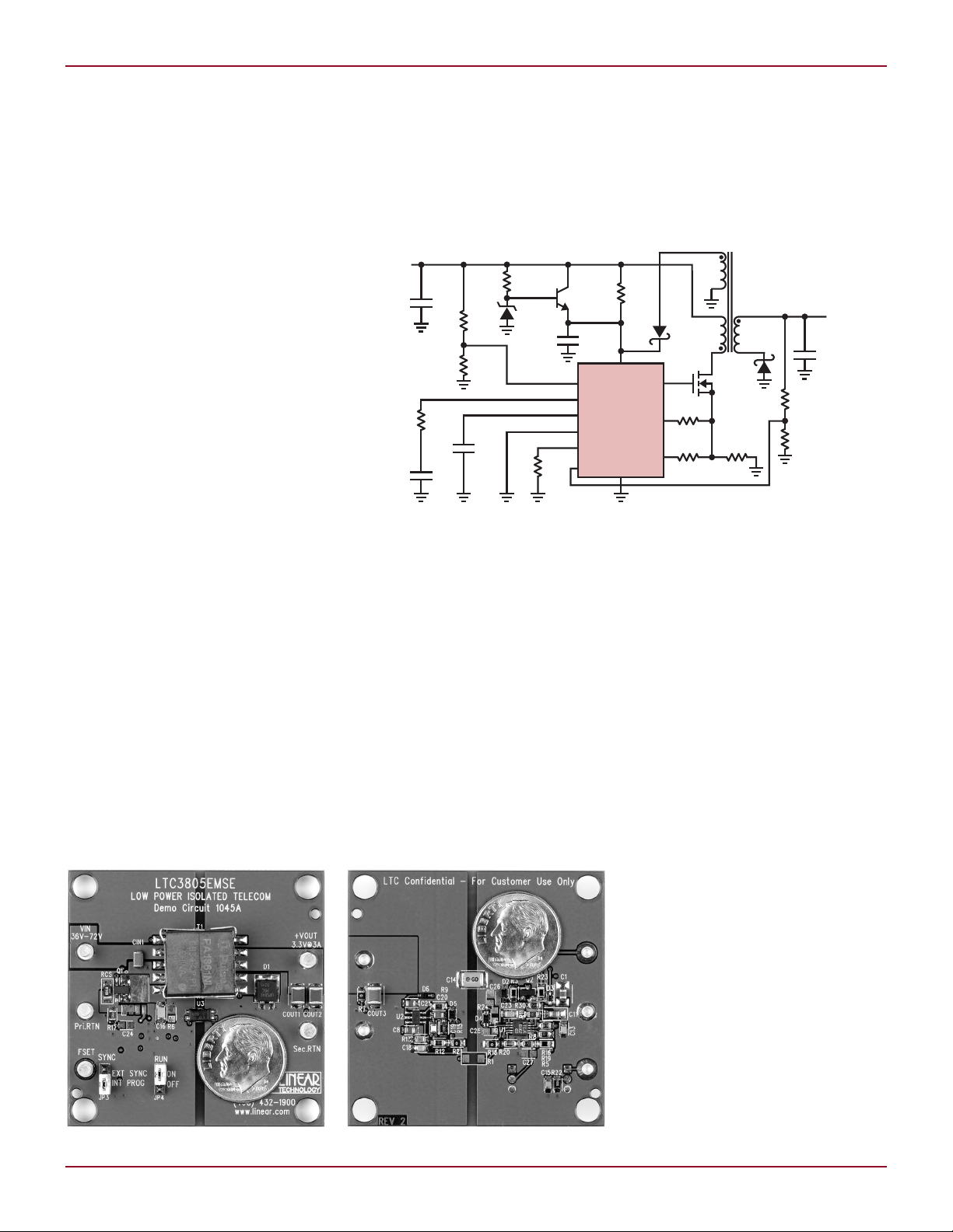
Figure 1 shows the LTC3805 in a
non-isolated flyback converter with
an input voltage range of 36V to 72V
and an output voltage of 3.3V at 3A.
The remainder of this section details
the design decisions made in creating
this converter and describes methods
for altering the design for various
applications. An isolated version of
the converter is described in the next
section.
VCC Power and Start-Up
In this design, start-up VCC power for
the LTC3805 is provided by an external
pre-regulator using an NPN transistor, a zener diode and two resistors.
Once the converter begins operation,
a winding on the transformer provides a bias supply which turns off
by Arthur Kelley
Figure 1. Non-isolated 36V to 72V to 3.3V 3A flyback converter
the NPN transistor to save power and
increase efficiency. Alternately, since
the LTC3805 has an ultralow shut
down current of 40µA, a simple trickle
charger could be used to eliminate the
NPN pre-regulator. The LTC3805 has
a VCC rising threshold of 8.5V and a
falling threshold of 4V so there is plenty
of hysteresis to implement a trickle
charger. In either case, note that VCC
is not connected to VIN so that almost
any input supply above 8.5V can be
accommodated by proper selection of
external components and that, once
started, the LTC3805 can run with
input supplies down to 4V.
-
Programming V
OUT
The FB pin monitors the output voltage by comparing it—via a resistive
divider—to the 0.8V internal reference
of the LTC3805. Since the FB pin is
not connected directly to the output,
8
Figure 2. Isolated 36V to 72V to 3.3V 3A flyback converter
the LTC3805 can accommodate any
output voltage down to 0.8V simply by
adjustment of the resistor values.
Selecting Frequency
The 200kHz operating frequency is
programmed by the 118k
Ω resistor
on the FS pin. By changing this resistor, the operating frequency can
Linear Technology Magazine • March 2007
DESIGN FEATURES L
I
OUT
(A)
0
0
EFFICIENCY (%)
20
30
40
50
60
70
1
2
80
90
100
10
3 4
36V
48V
60V
72V
V
IN
be set anywhere between 70kHz and
700kHz. High power designs tend to
use lower frequencies while low power
designs tend to use higher frequencies. The frequency programmability
of the LTC3805 allows selection of
the optimum frequency for any given
design.
Programming the VIN Thresholds
The rising threshold on VIN, which is
independent of the thresholds on VCC,
is set by the 221kΩ and 8.86kΩ resistors connected to the RUN pin. The
rising threshold on the RUN pin is 1.2V
while its absolute maximum voltage is
18V—a 15:1 ratio. Therefore the RUN
pin accommodates designs with a wide
range of input voltages and still has a
high enough voltage rating to survive
a transient overvoltage on VIN. Once
started, the LTC3805 sources a 5µA
current from the RUN pin. Multiplied
by the 221kΩ resistor, this current
sets the hysteresis on VIN to 1.1V. A
different hysteresis, with the same
rising threshold, can be selected by
changing the values of the 221kΩ and
8.86k
ratio constant.
Setting the Soft-Start
The rate of change of V
is programmed by the capacitor on the
SSFLT pin—0.1µF in this case. A major
consideration in the selection of the
SSFLT capacitor is the filter capacitor used to bypass V
larger output filter capacitor requires
a slower soft-start to limit the inrush
current caused by the charging filter
capacitor. Conversely, if the converter
has a small output filter capacitor, the
SSFLT capacitor can be omitted and
the LTC3805 internal soft-start ramps
up the output voltage in 1.8ms.
Programming Slope Compensation
and Overcurrent Operation
The 68m
rent through the main NMOS switch
and implements both current mode
control and overcurrent protection via
the I
The I
through the main switch and turns it
off when the current exceeds a level
Linear Technology Magazine • March 2007
Ω resistors while keeping their
at start-up
OUT
. Generally, a
OUT
Ω resistor monitors the cur-
and OC pins, respectively.
SENSE
pin monitors the current
SENSE
set by the voltage on the ITH pin. The
3.01kΩ resistor sets the amount of
slope compensation using a ramp
of current that is sourced by the
LTC3805.
The overcurrent protection level is
set by the 1.33kΩ resistor in series
with the OC pin using a constant 10µA
current sourced by the OC pin. Several
behaviors can be programmed using
this resistor. This particular design
is set to regulate output voltage up
present before the LTC3805 begins
operation or it can be applied after
the LTC3805 has begun operation
using the frequency programmed by
the resistor on the FS pin. When the
synchronization signal is applied,
the LTC3805 locks on to the signal
within two cycles of operation. When
the synchronization signal is removed,
the LTC3805 takes no more than two
cycles to jump back to the frequency
programmed by the FS pin.
to 3A and then overcurrent trip just
above that. An alternate strategy,
using a smaller resistor, would be to
allow the output voltage to sag as the
converter goes into current limiting
and then trip on overcurrent only
to prevent damage. In either case,
once there is an overcurrent trip the
LTC3805 shuts down, waits for a time
out interval determined by discharging the capacitor on the SSFLT pin
and then restarts if the overcurrent
fault has been removed. If the fault
is not removed, the LTC3805 enters
a hiccup mode in which it periodically
tries to restart with the period determined by the capacitor on the SSFLT
pin. Thusly, the LTC3805 completely
protects a flyback converter from short
circuits on the output.
Frequency Synchronization
to an External Source
Although shown grounded in Figure 1,
the SYNC pin is used to synchronize
the frequency of operation of the
LTC3805 to an external source. The
synchronization signal can be applied
and removed without any particular
sequencing requirement—it can be
Isolated Converter Design
The basic design shown in Figure 1
can be modified to provide DC isola-
tion between the input and output by
the addition of a reference, such as
the LT4430, on the secondary side of
the transformer and an optoisolator
to provide feedback from the isolated
secondary to the LTC3805. Figure
shows a photo of the DC1045 demon-
stration circuit, which is an isolated
converter with the same basic design
and performance as the converter
in Figure 1, and is representative of
the size of both the isolated and non-
isolated designs. Figure 3 shows the
efficiency of the isolated converter
and is also representative of the non-
isolated converter.
Modifications for Different
Input or Output Voltages
The two applications described above
represent typical non-isolated and
isolated 10W flyback converters. It is
fairly easy to take this basic design
and change the input or output voltage
by scaling the external components in
direct proportion to the change in volt-
age. These changes are transparent to
the LTC3805 and can be accomplished
with a circuit no more complex than
that of Figure 1 and a board no bigger
than that shown in Figure 2.
increase of the input current, mainly
involves selecting a NMOS power
switch with a lower voltage and higher
current rating and selecting a trans-
former primary winding with a reduced
number of turns and a proportionally
larger wire size. For the input filter
Figure 3. Efficiency for isolated and nonisolated 36V–72V to 3.3V 3A flyback converter
capacitor, the voltage rating can be
2
A decrease of the input voltage, and
continued on page 17
9

100ns/DIV
2V/DIV
B
A
DI
RO
Figure 8. The LTC2854 driver delivering a
single 50ns pulse through 100ft of Cat 5 cable,
which is received by another LTC2854. Both
parts have their on-chip termination enabled.
Top trace is the input to the transmitting
device and the middle and bottom traces are
observed at the receiving part.
to +15V, with typical peak current
not exceeding 180mA. Additionally,
thermal shutdown protection disables
the driver, receiver, and terminator if
excessive power dissipation causes
the device to heat to temperatures
above 160°C. When the temperature
drops below 140°C, normal operation
resumes.
Extreme ESD Protection
The driver output pins and receiver
input pins on the LTC2854 are pro
tected to ESD levels of ±25kV HBM
with respect to ground or VCC. The fullduplex LTC2855 withstands ±15kV
ESD. These protection levels exist for
all modes of device operation including
power-down, standby, receive, transmit, termination and all combinations
of these. Furthermore, the protection
level is valid whether VCC is on, shorted
to ground, or disconnected.
When a line I/O pin on the
LTC2854/LTC2855 is hit with an
-
DESIGN FEATURES L
Figure 9. The LTC2854 sending data (see scope traces in background)
while hit with multiple 30kV ESD strikes on the ‘A’ pin.
ESD strike during operation, the part
undergoes a short disturbance of duration similar to the ESD event and
then fully recovers. The device does
not latch up and there is no need to
toggle states or cycle the supply to
recover. This is true whether the part
is in a static state or sending/receiving
data and for the full range of ground
common mode voltages called out in
the RS485 standard. The photo in Fig
ure 9 shows the LTC2854 absorbing
the energy from an ESD gun (configured for IEC air discharge) delivering
repeated 30kV strikes to the ‘A’ pin
while transmitting data. The oscilloscope traces in the background show
data toggling happily on the A and B
pins before and after a strike, with a
positive glitch only during the ESD
-
event. This device can handle many
such strikes without damage.
Conclusion
The LTC2854 and LTC2855 break
new ground in the world of 3.3V
RS485/RS422 transceivers. The in
clusion of a selectable termination
resistor provides a complete solution
to RS485 networking with the ability
to remotely configure the network
for optimal data transfer. Unparal-
leled ESD performance provides
outstanding ruggedness while a bal-
anced-threshold receiver with full
failsafe capability makes this family
of small-footprint devices a natural
choice for modern RS485/RS422
systems.
L
-
LTC3805, continued from page 9
reduced and the capacitance increased
in proportion. Also, the resistor divider
connected to the RUN pin must be
adjusted for the new input voltage.
Finally, the 68m
Ω current sense resistor should be reduced in value to
account for the higher input current.
For an increase in input voltage, everything is changed proportionally in
the opposite direction.
Similarly, a change in the output
voltage involves a change in the diode,
Linear Technology Magazine • March 2007
the number of turns in the secondary
winding of the transformer and the
voltage rating and value of the output
filter capacitor along with the appropriate change to the voltage divider
that senses the output voltage. If the
output voltage is between 4V and 9V,
the design of non-isolated converters
is very simple because VCC can be provided by a diode connected directly to
the output instead of the third winding
on the transformer.
Conclusion
Because of its flexibility, the flyback
converter is the most widely used
transformer-based converter. The
LTC3805 maximizes the flexibility of
the flyback converter by making it possible to use the same basic circuit for a
wide range of converter input and output voltages. Simply scale component
values to match voltage and current
conditions, greatly simplifying board
design and updates.
L
17
 Loading...