

Programmable Up/Down Tracking
FEATURES
■
Wide VIN Range: 3V to 30V Operation with Line
Feedforward Compensation
■
Leading Edge Modulation Architecture for
Extremely Low Duty Cycle Operation
■
Phase-Lockable Fixed Frequency: 330kHz to 750kHz
■
Two 180° Out-of-Phase Controllers
■
Fast Programmable Power-Up/-Down Tracking
■
Programmable Current Limit Without External
Current Sense Resistor
■
Optional Burst Mode® Operation at Light Load
■
±1% 0.6V Voltage Reference
■
External N-Channel MOSFET Architecture
■
Low Shutdown Current: <100µA
■
Overvoltage Protection and PGOOD Flag
■
Small 28-Lead SSOP and 32-Lead QFN Packages
U
APPLICATIO S
■
Notebook and Palmtop Computers
■
Portable Instruments
■
Battery-Operated Digital Devices
■
DC Power Distribution Systems
LTC3802
Dual 550kHz Synchronous
2-Phase DC/DC Controller with
U
DESCRIPTIO
The LTC®3802 is a dual switching regulator controller
optimized for high efficiency step-down conversion from
input voltages between 3V to 30V. The controller uses a
leading edge modulation scheme to allow extremely low
duty cycle operation. The constant frequency voltage mode
controller allows a phase-lockable frequency between
330kHz and 750kHz. Power loss and noise due to the ESR
of the input capacitors are minimized by operating the two
controller output stages 180° out of phase. The synchronous buck architecture automatically shifts to Burst Mode
operation as the output load decreases, ensuring maximum efficiency over a wide range of load currents.
The LTC3802 features an onboard, trimmed 0.6V reference and provides better than 1% regulation at the converter outputs. A separate output sense provides real time
overvoltage protection and PGOOD sensing. An FBT pin
programs the power-up/-down tracking between the two
channels to meet various sequencing requirements. A
RUN/SS pin provides soft-start and externally programmable current limit protection functions.
, LTC and LT are registered trademarks of Linear Technology Corporation.
Burst Mode is a registered trademark of Linear Technology Corporation.
U.S. Patent Nos 5481178, 5846544, 6304066, 6580258, 5055767, 6307356
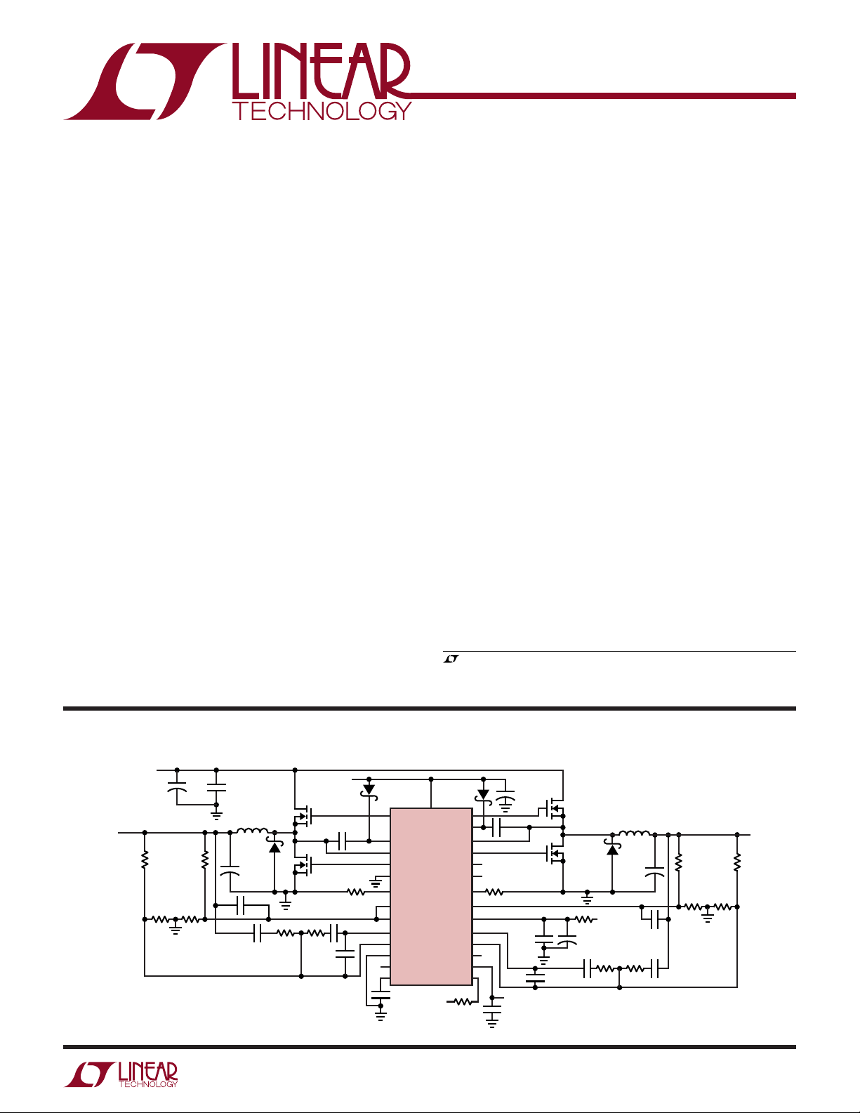
TYPICAL APPLICATIO
V
IN
V
OUT1
3.3V
15A
5V TO 22V
10k
56µF
+
2.21k2.21k
10k
25V
×2
4.7µF
25V
×8
+
1500pF
1µH
B340B
330µF
4V
×3
560pF
390Ω
U
CMDSH-3
Si7860DP
×2
Si7440DP
×2
15k
330pF
5V
0.1µF
2200pF
TG1
BOOST1
SW1
BG1
PGND
I
MAX1
FBT
CMPIN1
COMP1
FB1
SGND
FCB
RUN/SS
0.1µF
PV
CC
LTC3802
CMDSH-3
TG2
BOOST2
SW2
BG2
PLLIN
PLLLPF
I
MAX2
CMPIN2
V
COMP2
FB2
PHASEMD
V
INFF
PGOOD
10k
5V
+
10µF
0.1µF
47k47k
CC
0.1µF
V
IN
0.47µF
330pF
Si7860DP
×2
Si7440DP
×2
+
10Ω
10µF
1µH
B340B
330µF
4V
×3
5V
390Ω15k
+
560pF
1500pF2200pF
10k
3.16k 3.16k
10k
3802 TA01
V
2.5V
15A
OUT2
3802f
1
LTC3802
WW
W
U
ABSOLUTE AXI U RATI GS
Supply Voltage
VCC, PVCC............................................................. 7V
BOOSTn.............................................................. 37V
BOOSTn – SWn.................................................... 7V
SWn........................................................ –1V to 30V
Input Voltage
V
.................................................................... 30V
INFF
FBn, CMPINn, FBT, PLLIN, FCB,
RUN/SS, PGOOD, PLLLPF, PHASEMD,
EXTREF, I
n
.......................... –0.3V to VCC + 0.3V
MAX
UUW
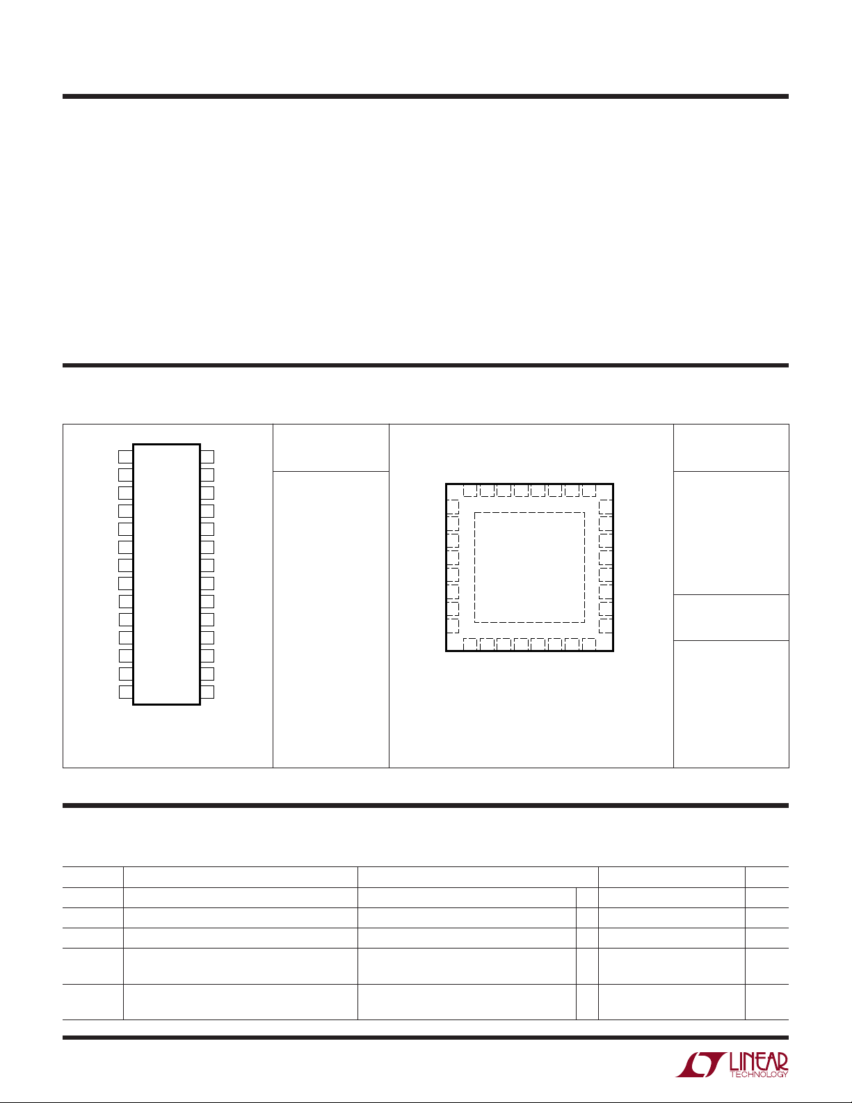
PACKAGE/ORDER I FOR ATIO
PV
CC
BG1
BOOST1
TG1
SW1
PGND
I
MAX1
FBT
CMPIN1
10
COMP1
11
FB1
12
SGND
13
FCB
14
RUN/SS
28-LEAD PLASTIC SSOP
T
JMAX
TOP VIEW
1
2
3
4
5
6
7
8
9
GN PACKAGE
= 125°C, θJA = 110°C/W
28
27
26
25
24
23
22
21
20
19
18
17
16
15
BG2
BOOST2
TG2
SW2
PLLIN
PLLLPF
I
MAX2
CMPIN2
V
CC
COMP2
FB2
PHASEMD
V
INFF
PGOOD
ORDER PART
NUMBER
LTC3802EGN
(Note 1)
PGND
PGND
I
MAX1
FBT
CMPIN1
COMP1
FB1
Extended Commercial
Operating Temperature Range (Note 2) .. –40°C to 85°C
Storage Temperature Range
LTC3802EGN ................................... –65°C to 150°C
LTC3802EUH ................................... –65°C to 125°C
Lead Temperature (Soldering, 10 sec)
LTC3802EGN Only........................................... 300°C
TOP VIEW
ORDER PART
NUMBER
TG1
BOOST1
BG1
PVCCBG2
BOOST2
TG2
32 31 30 29 28 27 26 25
1SW1
2
3
4
5
6
7
8
9 10 11 12
SGND
32-LEAD (5mm × 5mm) PLASTIC QFN
T
JMAX
EXPOSED PAD (PIN 33) IS GND
MUST BE SOLDERED TO PCB
33
13 14 15 16
FCB
PGOOD
EXTREF
RUN/SS
UH PACKAGE
= 125°C, θJA = 34°C/W
V
INFF
PHASEMD
SW2
FB2
24
23
22
21
20
19
18
17
PGND
PGND
PLLIN
PLLLPF
I
MAX2
CMPIN2
V
CC
COMP2
LTC3802EUH
UH PART
MARKING
3802
Consult LTC Marketing for parts specified with wider operating temperature ranges.
ELECTRICAL CHARACTERISTICS
The ● denotes the specifications which apply over the full operating
temperature range. (Note 3) VCC = PVCC = BOOST = 5V, unless otherwise specified.
SYMBOL PARAMETER CONDITIONS MIN TYP MAX UNITS
V
PV
BV
V
I
VCC
CC
CC
CC
UVLO
VCC Supply Voltage ● 356 V
PVCC Supply Voltage (Note 4) ● 56 V
BOOST Pin Voltage V
Positive Undervoltage Lockout Measured at V
VCC Supply Current VFB = V
– VSW (Note 4) ● 56 V
BOOST
Measured at V
V
RUN/SS
CC
INFF
COMP
= 0V, PLLIN Floating ● 100 150 µA
2.2 2.5 2.8 V
2.2 2.5 2.8 V
● 6.5 9 mA
3802f
2
LTC3802
ELECTRICAL CHARACTERISTICS
The ● denotes the specifications which apply over the full operating
temperature range. (Note 3) VCC = PVCC = BOOST = 5V, unless otherwise specified.
SYMBOL PARAMETER CONDITIONS MIN TYP MAX UNITS
I
PVCC
I
BOOST
Switcher Control Loop
V
FB
∆V
FB
∆V
OUT
A
ERR
GBW Error AMP Gain Bandwidth Product f = 100kHz (Note 7) 10 MHz
I
COMP
I
FB
I
CMPIN
I
FBT
I
EXTREF
V
EXTREF
A
LFF
R
VINFF
V
PGOOD
V
OVP
V
BURRS
V
SAW
I
IMAX
I
LIM(TH)
I
SS
V
SHDN
LOGIC and PGOOD
I
PHASEMD
V
IH
V
IL
I
PGOOD
V
OLPG
t
PGOOD
PVCC Supply Current VFB = V
V
RUN/SS
BOOST Pin Current VFB = V
V
RUN/SS
Feedback Voltage V
EXTREF
V
EXTREF
= 0V, No Load 2 mA
CMPIN
= 0V (Notes 5, 6) 1 10 µA
= 0V, No Load 1 mA
CMPIN
= 0V (Notes 5, 6) 1 10 µA
= 5V, 0°C ≤ T ≤ 70°C 0.594 0.600 0.606 V
= 5V ● 0.591 0.600 0.609 V
Feedback Voltage VCC Line Regulation VCC = 4.5V to 6V ±0.01 %/V
Output Voltage Load Regulation (Note 7) 0.1 ±0.2 %
Error AMP DC Gain No Load, V
Error AMP Output Sink/Source Current V
RUN/SS
= V
EXTREF
CC
= V
RUN/SS
= V
CC
● 70 80 dB
±12 mA
Voltage Feedback Input Current VFB = 0V to 1V ● ±1 µA
Comparators Input Current V
FBT Input Current V
EXTREF Input Current V
External Reference Not to Affect V
∆ Drop in Duty Cycle/∆ V
V
Input Resistance 1MΩ
INFF
FB
INFF
= 0V to 1V ● ±1 µA
CMPIN
= 0V to 1V ● ±1 µA
FBT
= 0V to 5V ● ±1 µA
EXTREF
● 1V
V
= 5V to 30V 2.3 %/V
VINFF
Positive Power Good Threshold With Respect to 0.6V ● 5 10 15 %
Negative Power Good Threshold With Respect to 0.6V
Overvoltage Threshold With Respect to V
(V
– VFB) to Reset 15 mV
CMPIN
FB
● –5 –10 –15 %
359 %
Burst Mode Operation –12 mV
SAW Before Line Compensation 1.2 V
I
Source Current V
MAX
I
Comparator Offset ● –15 0 15 mV
LIM
V
Hard I
Threshold 5V/V
IMAX/ILIM
Threshold V
LIM/ILIM
RUN/SS Source Current V
RUN/SS Sink/Source Current Ratio V
RUN/SS Sink Current, I
RUN/SS Sink Current, Hard I
LIM
LIM
= 1V –9.0 –10 –11.0 µA
IMAX
= 0V 1.5 V/V
CMPIN
= V
CMPIN
CMPIN
V
CMPIN
V
CMPIN
= 0.6V, V
FBT
= V
= 0.6V, V
FBT
= V
= 0.6V 100 µA
FBT
= V
= 0V ● 1mA
FBT
= V
PHASEMD
PHASEMD
CC
= 0V 1.5 2 2.5 µA/µA
● –8.5 –10 –11.5 µA
–5 –7 –9 µA
RUN/SS Shutdown Threshold RUN/SS↑ ● 0.4 0.8 1.2 V
PHASEMD Pull-Up Current V
PHASEMD Pull-Down Current V
= 0V –7 µA
PHASEMD
= 5V 2 µA
PHASEMD
PLLIN, FCB High Level Input Voltage ● 2.4 V
PLLIN, FCB Low Level Input Voltage ● 0.8 V
V
Leakage Current Power Good ±1 µA
PGOOD
V
Output Low Voltage I
PGOOD
V
Falling Edge Delay (Note 8) ● 100 150 µs
PGOOD
V
Rising Edge Delay (Note 8) 10 µs
PGOOD
= 1mA ● 0.1 0.3 V
PGOOD
3802f
3
LTC3802
ELECTRICAL CHARACTERISTICS
The ● denotes the specifications which apply over the full operating
temperature range. (Note 3) VCC = PVCC = BOOST = 5V, unless otherwise specified.
SYMBOL PARAMETER CONDITIONS MIN TYP MAX UNITS
Switcher Switching Characteristics
f
OSC
R
PLLIN
I
PLLLPF
Phase TG1↓ vs PLLIN↓ PHASEMD Floats 0 Deg
V
PHASEMD
DC
MIN
DC
MAX
t
ON(MIN)
t
NOV
R
DS(ON)
Oscillator Frequency PLLIN Open or V
V
= 1.2V 550 kHz
PLLLPF
V
= 0V 250 330 400 kHz
PLLLPF
V
= 2.4V 650 750 850 kHz
PLLLPF
= 0V 490 550 610 kHz
PLLIN
PLLIN Pull-Down Current Source 5 µA
Phase Detector Output Current
Sourcing Capability f
Sinking Capability f
TG1↓ vs PLLIN↓ V
> f
PLLIN
< f
PLLIN
PHASEMD
OSC
OSC
–15 µA
15 µA
= 5V 90 Deg
TG2↓ vs PLLIN↓ PHASEMD Floats 180 Deg
TG2↓ vs PLLIN↓ V
= 5V 270 Deg
PHASEMD
Shutdown Threshold ● 1.2 1.7 V
Floating 2.0 V
90° Phase Threshold ● 3.5 4.0 4.5 V
Minimum TG Duty Cycle V
Maximum TG Duty Cycle V
= 0V ● 0%
PLLIN
PLLIN
= 0V, V
= 0.6V (Note 9) ● 86 89 92 %
CMPIN
TG Minimum Pulse Width (Notes 7, 10) 50 ns
BG Minimum Pulse Width V
= 0V (Note 9) 400 ns
CMPIN
Driver Nonoverlap No Load 10 30 80 ns
TG High R
TG Low R
BG High R
BG Low R
DS(ON)
DS(ON)
DS(ON)
DS(ON)
I
= 100mA (Note 7) 1.6 2.20 Ω
OUT
1.3 1.80 Ω
1.8 2.50 Ω
0.7 1.00 Ω
Note 1: Absolute Maximum Ratings are those values beyond which the life
of a device may be impaired.
Note 2: The LTC3802 is guaranteed to meet performance specifications
from 0°C to 70°C. Specifications over the –40°C to 85°C operating
temperature range are assured by design, characterization and correlation
with statistical process controls.
Note 3: All currents into device pins are positive; all currents out of device
pins are negative. All voltages are referenced to ground unless otherwise
specified.
Note 4: To ensure proper operation, PV
be greater than V
of the external MOSFETs.
GS(ON)
and BVCC (V
CC
BOOST
– VSW) must
Note 5: Supply current in normal operation is dominated by the current
needed to charge and discharge the external MOSFET gates. This current
will vary with supply voltage and the external MOSFETs used.
Note 6: Supply current in shutdown is dominated by external MOSFET
leakage and may be significantly higher than the quiescent current drawn
by the LTC3802, especially at elevated temperature.
Note 7: Guaranteed by design, not subject to test.
Note 8: Rise and fall times are measured using 10% and 90% levels. Delay
and nonoverlap times are measured using 50% levels.
Note 9: If V
is less than 90% of its nominal value, BG minimum
CMPIN
pulse width is limited to 400ns.
Note 10: The LTC3802 leading edge modulation architecture does not
have a minimum TG pulse width requirement. The TG minimum pulse
width is limited by the rise and fall times.
3802f
4
UW
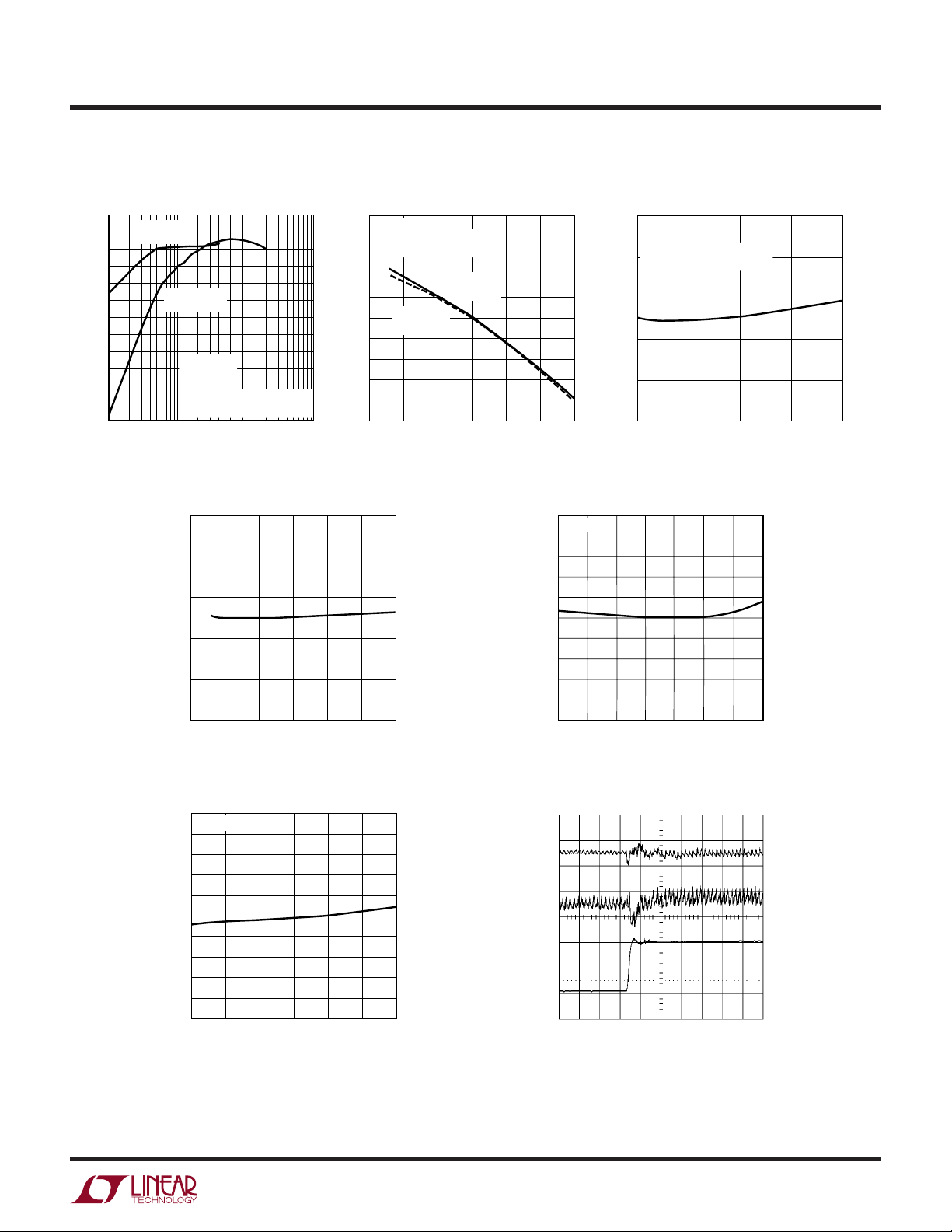
TYPICAL PERFOR A CE CHARACTERISTICS
LTC3802
Efficiency vs I
100
EFFICIENCY (%)
Burst Mode
95
OPERATION
90
85
80
75
70
65
60
55
50
45
40
0.1
OUT
CONTINUOUS
MODE
VIN = 12V
V
= 3.3V
OUT
T
= 25°C
A
CIRCUIT ON THE FIRST PAGE
OF THIS DATA SHEET
1 10 100
I
(A)
OUT
Line Regulation
2.5125
VCC = 5V
= 5A
I
OUT
= 25°C
T
2.5075
2.5025
(V)
OUT
V
2.4975
2.4925
2.4875
A
0
10 15 20
5
3802 G01
VIN (V)
Efficiency vs V
100
TA = 25°C
98
CIRCUIT ON THE FIRST PAGE
OF THIS DATA SHEET
96
94
92
V
= 2.5V
0
25 30
3802 G04
OUT
I
OUT
5
0.5
0.4
0.3
0.2
0.1
0
–0.1
–0.2
–0.3
–0.4
–0.5
= 10A
∆V
OUT
(%)
90
88
EFFICIENCY (%)
86
84
82
80
IN
V
= 2.5V
OUT
I
= 5A
OUT
15 20
10
VIN (V)
30
25
3802 G02
Load Regulation
2.5125
VIN = 12V
= 25°C
T
A
CIRCUIT ON THE FIRST PAGE
2.5075
OF THIS DATA SHEET
2.5025
(V)
OUT
V
2.4975
2.4925
2.4875
0
0.5
0.4
0.3
0.2
∆V
0.1
OUT
0
(%)
–0.1
–0.2
–0.3
–0.4
3802 G03
–0.5
20
I
OUT
10
15
(A)
5
VFB vs Temperature
100
125
1.0
0.8
0.6
0.4
0.2
0
–0.2
–0.4
–0.6
–0.8
–1.0
∆V
FB
(%)
606.0
604.8
603.6
602.4
601.2
600.0
(mV)
FB
V
598.8
597.6
596.4
595.2
594.0
VCC = 5V
–50
0
–25
TEMPERATURE (°C)
50
25
75
LTC1323 • TPC05
VFB vs VCC Supply Voltage Line Feedforward Transient
3802 G06
0.5
0.4
0.3
0.2
∆V
0.1
FB
(%)
0
–0.1
–0.2
–0.3
–0.4
–0.5
6
V
OUT
2.5V
(NO LOAD)
AC 50mV/DIV
V
COMP
AC 50mV/DIV
V
5V TO 15V
STEP
5V/DIV
IN
: 1µF/50V ×6
C
IN
SANYO 35CV220AX
10µs/DIV
603.0
602.4
601.8
601.2
600.6
600.0
(mV)
FB
V
599.4
598.8
598.2
597.6
597.0
TA = 25°C
3
4.5
4
3.5
VCC SUPPLY VOLTAGE (V)
5
5.5
3802 G07
3802f
5
LTC3802
TEMPERATURE (°C)
–50 –25
–10
I
LIM(TH)
OFFSET (mV)
–2
10
0
50
75
3802 G13
–6
6
2
25
100
125
VCC = 5V
V
IMAX
= 500mV
UW
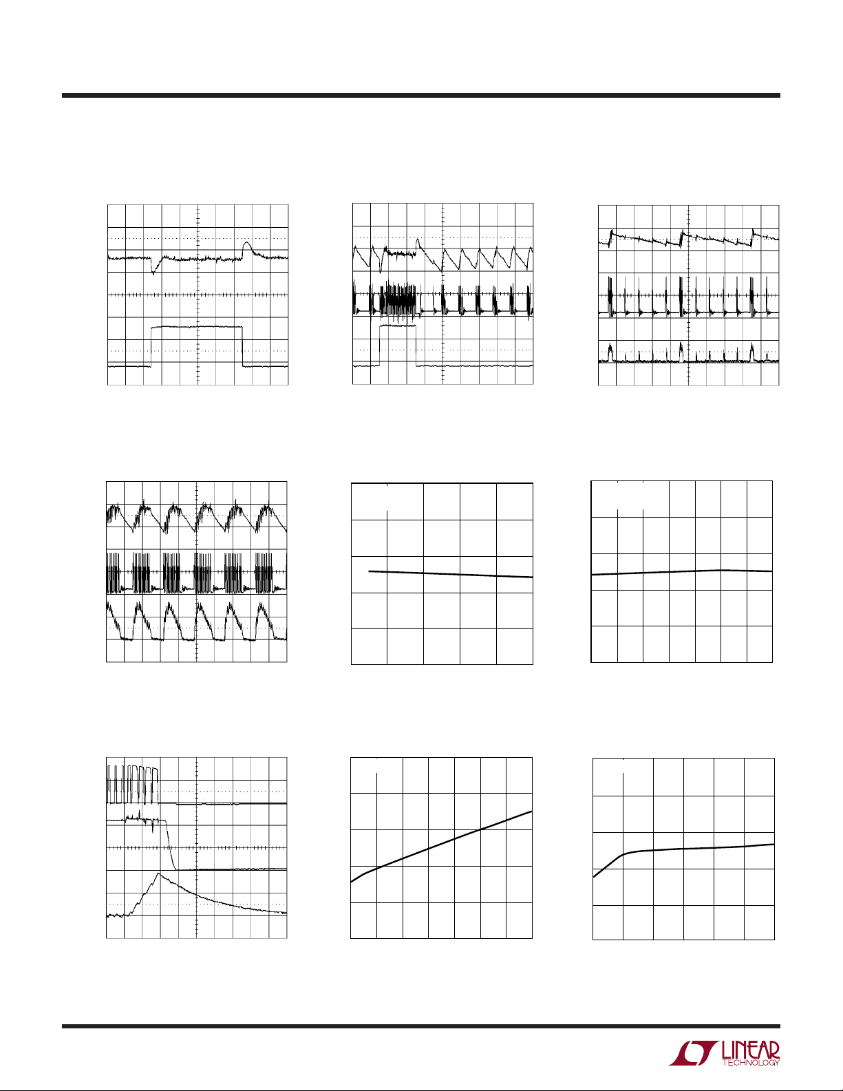
TYPICAL PERFOR A CE CHARACTERISTICS
V
OUT
1.2V
50mV/DIV
Load Step in Continuous Mode
50mV/DIV
Load Step in Burst Mode Operation
V
OUT
1.2V
V
SW
10V/DIV
V
OUT
1.2V
50mV/DIV
V
SW
10V/DIV
Burst Mode Waveform
with 0.2A Load
I
OUT
1A TO 10A
STEP
5A/DIV
V
OUT
1.2V
50mV/DIV
V
10V/DIV
INDUCTOR
CURRENT
5A/DIV
10V/DIV
= 12V
IN
CIRCUIT ON
FIRST PAGE OF THIS DATA SHEET
20µs/DIVV
Burst Mode Waveform
with 3A Load
SW
= 12V
IN
CIRCUIT ON
FIRST PAGE OF THIS DATA SHEET
20µs/DIVV
Short-Circuit Test
TG
3802 G08
3802 G11
I
OUT
1A TO 10A
STEP
5A/DIV
10
OFFSET (mV)
LIM(TH)
I
–6
–10
600
580
= 12V
IN
CIRCUIT ON
FIRST PAGE OF THIS DATA SHEET
I
LIM(TH)
TA = 25°C
= 5V
V
CC
6
2
–2
200
0
50µs/DIVV
Offset vs V
400
V
IMAX
Switching Frequency
vs Temperature
VCC = 5V
IMAX
600
(mV)
800
3802 G09
3802 G12
1000
INDUCTOR
CURRENT
5A/DIV
= 12V
IN
CIRCUIT ON
FIRST PAGE OF THIS DATA SHEET
I
LIM(TH)
Switching Frequency
vs VCC Supply Voltage
600
TA = 25°C
580
50µs/DIVV
Offset vs Temperature
3802 G10
RUN/SS
2V/DIV
INDUCTOR
CURRENT
20A/DIV
6
CIRCUIT ON
FIRST PAGE OF THIS DATA SHEET
= 12V, V
V
IN
= 47k, L = 1µH (TOKO-FDA1254-1ROM)
R
I(MAX)
5µs/DIV
= 3.3V, CSS = 0.01µF,
OUT
3802 G14
560
540
520
SWITCHING FREQUENCY (kHz)
500
–50 –25
25
0
TEMPERATURE (°C)
560
540
SWITCHING FREQUENCY (kHz)
520
50
75
100
125
3802 G15
500
3
4 4.5 5
3.5
VCC SUPPLY VOLTAGE (V)
5.5 6
3802 G16
3802f
UW
TEMPERATURE (°C)
–50
MAXIMUM DUTY CYCLE (%)
95
25
3802 G19
80
70
–25 0 50
65
60
100
90
85
75
75 100 125
VCC = 5V
f
SW
= 550kHz
V
CMPIN
> 0.54V
V
CMPIN
< 0.54V
TYPICAL PERFOR A CE CHARACTERISTICS
Switching Frequency vs V
850
TA = 25°C
= 5V
V
CC
750
PLLLPF
AC 20mV/DIV
Continuous Mode Operation
V
OUT1
5V
LTC3802
Maximum Duty Cycle
vs Temperature
650
550
450
SWITCHING FREQUENCY (kHz)
350
250
0
0.8 1.2 1.6
0.4
V
PLLLPF
Maximum Duty Cycle
vs VCC Supply Voltage
100
TA = 25°C
= 550kHz
f
SW
95
90
85
80
75
70
MAXIMUM DUTY CYCLE (%)
65
0
3
V
CMPIN
V
< 0.54V
CMPIN
3.5 4 5
VCC SUPPLY VOLTAGE (V)
(V)
> 0.54V
4.5
2 2.4
3802 G17
5.5
3802 G20
6
TG1
20V/DIV
V
OUT2
TG2
20V/DIV
1V
= 30V
IN
AC 20mV/DIV
Maximum Duty Cycle
vs Switching Frequency Duty Cycle vs V
100
TA = 25°C
= 5V
V
CC
95
90
85
80
75
70
MAXIMUM DUTY CYCLE (%)
65
60
390 450 570
330
0.5µs/DIVV
V
> 0.54V
CMPIN
V
< 0.54V
CMPIN
510
SWITCHING FREQUENCY (kHz)
630 690 750
3802 G18
3802 G21
100
90
VIN = 5V
80
VIN = 12V
70
60
50
40
DUTY CYCLE (%)
30
20
10
0
0.8
1 1.4
1.2
V
COMP
1.6
COMP
(V)
1.8
VIN = 30V
VIN = 20V
TA = 25°C
= 5V
V
CC
V
CMPIN
2
= V
2.2
FB
2.4
3802 G22
I
IMAX
vs Temperature
12.0
VCC = 5V
11.5
11.0
10.5
(µA)
10.0
IMAX
I
9.5
9.0
8.5
8.0
–50
–25 0 50
and I
RUN/SS
TEMPERATURE (°C)
I
RUN/SS
SINK CURRENT
I
IMAX
I
RUN/SS
SOURCE CURRENT
25
75 100 125
3802 G23
20
15
10
5
0
–5
–10
–15
–20
I
RUN/SS
(µA)
(µA)
IMAX
I
11.5
10.9
10.3
9.7
9.1
8.5
I
vs VCC Supply Voltage
IMAX
TA = 25°C
3
4 4.5 5
3.5
VCC SUPPLY VOLTAGE (V)
5.5 6
3802 G24
Driver Supply Current vs Load
80
TA = 25°C
= V
PV
CC
60
40
20
DRIVER SUPPLY CURRENT (mA)
0
0
– VSW = 5V
BOOST
2000
4000
CTG, CBG LOAD (pF)
6000
I
PVCC
I
BOOST1
I
BOOST2
8000
10000
3802 G25
3802f
7
LTC3802
UW
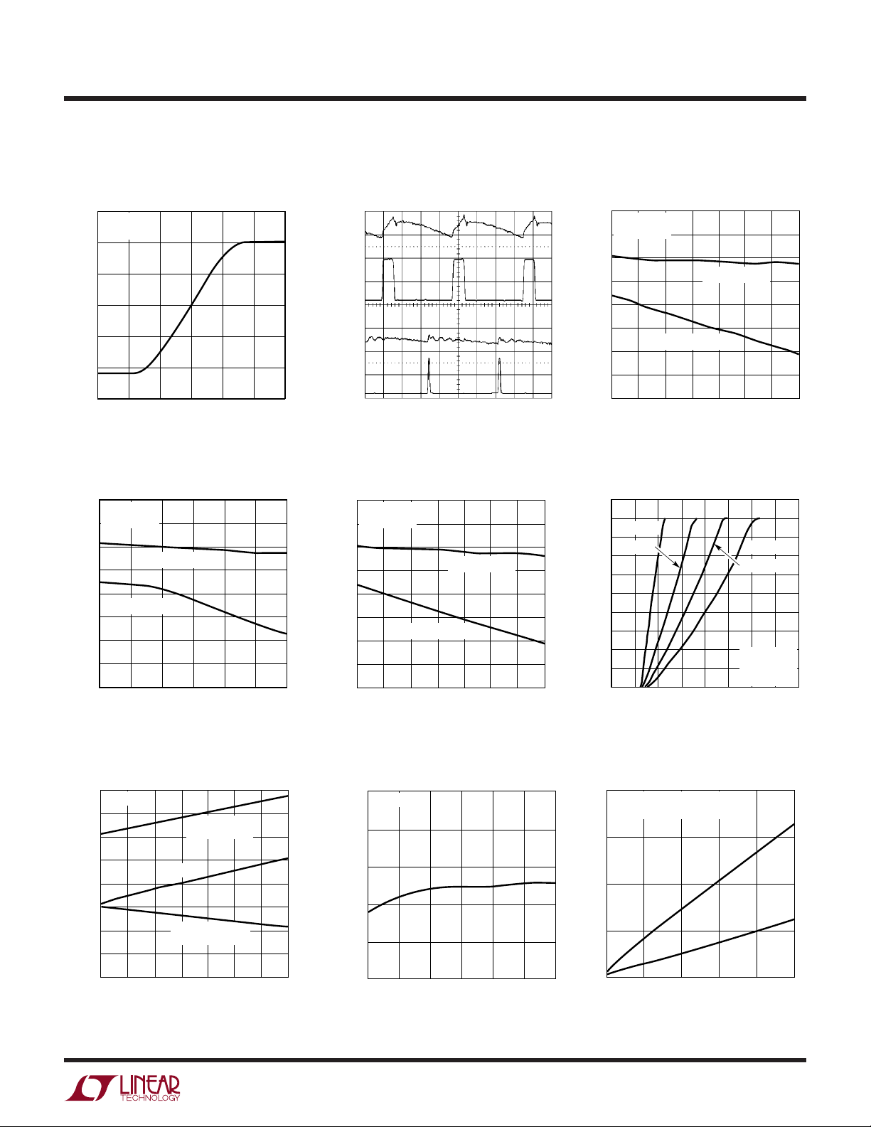
TYPICAL PERFOR A CE CHARACTERISTICS
Supply Current vs Temperature Supply Current vs Supply Voltage
10
I
VCC
1
I
PVCC
(NO LOAD)
I
BOOST1
I
BOOST2
(NO LOAD)
10
1
TA = 25°C
I
PVCC
(NO LOAD)
I
VCC
I
BOOST1, IBOOST2
(NO LOAD)
0.1
SUPPLY CURRENT (mA)
0.01
VCC = V
–50 –25
= V
PVCC
0 25 50 75 100 125
TEMPERATURE (°C)
BOOST
I
SHUTDOWN
– VSW = 5V
VCC
3802 G26
UUU
PI FU CTIO S
PVCC (Pin 1/Pin 29): Driver Power Supply Input. PV
provides power to the two BG drivers and must be connected to an external voltage high enough to fully turn on
the external MOSFETs, QB1 and QB2. PVCC requires at
least a 10µF bypass capacitor directly to PGND.
BG1 (Pin 2/Pin 30): Channel 1 Controller Bottom Gate
Drive. The BG1 pin drives the gate of the bottom N-channel
synchronous switch MOSFET, QB1. BG1 is designed to
drive typically up to 10,000pF of gate capacitance.
BOOST1 (Pin 3/Pin 31): Channel 1 Controller Top Gate
Driver Supply. BOOST1 should be bootstrapped to SW1
with a 0.1µF capacitor. An external Schottky diode from
PVCC to BOOST1 creates a complete floating chargepumped supply at BOOST1. No other external supplies are
required.
TG1 (Pin 4/Pin 32): Channel 1 Controller Top Gate Drive.
The TG1 pin drives the top N-channel MOSFET with a
voltage swing equal to PVCC superimposed on the switch
node voltage SW1. TG1 is designed to drive typically up to
6000pF of gate capacitance.
(28-Pin SSOP/32-Pin QFN Package)
CC
0.1
SUPPLY CURRENT (mA)
0.01
3
I
SHUTDOWN
VCC
453.5 4.5 5.5 6
SUPPLY VOLTAGE (V)
3802 G27
SW1 (Pin 5/Pin 1): Channel 1 Controller Switching Node.
Connect SW1 to the switching node of the channel 1
converter. When the bottom MOSFET QB1 turns on, the
current limit comparator and the burst comparator
monitor the voltage at SW1. If the voltage drop across
MOSFET QB1 is too large, the controller enters current
limit; if it is too small, the switcher enters Burst Mode
operation. See Current Limit and Burst Mode Applications Information.
PGND (Pin 6/Pins 2, 3, 23, 24): Power Ground. The BG
drivers return to this pin. Connect PGND to a high current
ground node in close proximity to the sources of external
MOSFETs QB1 and QB2 and the VIN, PVCC and V
OUT
bypass capacitors.
I
(Pin 7/Pin 4): Channel 1 Controller Current Limit
MAX1
Set. The I
pin has an internal 10µA current source
MAX1
pull-up, allowing the current limit and burst comparator
threshold to be programmed by a single external resistor
to SGND. See Current Limit and Burst Mode Applications
Information.
8
3802f

UUU
PI FU CTIO S
LTC3802
(28-Pin SSOP/32-Pin QFN Package)
FBT (Pin 8/Pin 5): Feedback Tracking Input. FBT should be
connected through a resistive divider network to V
set the channel 1 output slew rate. Upon power-up/-down,
the LTC3802 servos FBT and CMPIN2 to the same potential to control the output power-up/-down slew rate. To
program both outputs to have the same slew rate, duplicate the CMPIN2 resistive divider at FBT. To have a
ratiometric slew rate, short FBT to CMPIN1. To disable the
tracking function, short FBT to CMPIN2.
CMPIN1 (Pin 9/Pin 6): Channel 1 Controller Comparators
Input. CMPIN1 should be connected through a resistive
divider network to V
voltage. To improve transient response, a feedforward
capacitor can be added to the resistive divider. The power
good comparators, overvoltage comparator and Burst
reset comparators monitor this node directly. CMPIN1 is
a sensitive pin, avoid coupling noise into this pin.
COMP1 (Pin 10/Pin 7): Channel 1 Controller Error Amplifier Output. The COMP1 pin is connected directly to the
channel 1 error amplifier output and the input of the line
feedforward circuit. Use an RC network between the
COMP1 pin and the FB1 pin to compensate the feedback
loop for optimum transient response. Under start-up
conditions, the potential at RUN/SS controls the slew rate
at COMP1.
FB1 (Pin 11/Pin 8): Channel 1 Controller Error Amplifier
Input. FB1 should be connected through a resistive divider
network to V
voltage. Also, connect the channel 1 switcher loop compensation network to FB1.
SGND (Pin 12/Pin 9): Signal Ground. All the internal low
power circuitry returns to the SGND pin. Connect to a low
impedance ground, separated from the PGND node. All
feedback, compensation and soft-start connections should
return to SGND. SGND and PGND should be connected
only at a single point, near the PGND pin and the negative
terminal of the VIN bypass capacitor.
to set the channel 1 switcher output
OUT1
to monitor its real time output
OUT1
OUT1
to
FCB (Pin 13/Pin 10): Force Continuous Bar. Internally
pulled high. When FCB is shorted to GND, the controller
forces both converters to maintain continuous synchronous operation regardless of load current.
EXTREF (Pin 11, QFN Package Only): External Reference.
The EXTREF pin and the internal bandgap voltage are used
as the switcher control loop’s reference in a diode OR
manner. If the potential at the EXTREF pin is less than 0.6V,
it overrides the internal reference and lowers the switcher
output voltages. If EXTREF potential is more than 1V, the
internal bandgap voltage controls both channel output
voltages. EXTREF has no effect on the PGOOD threshold.
EXTREF is internally connected to the RUN/SS pin in the
GN28 package.
RUN/SS (Pin 14/Pin 12): Run Control and Soft-Start
Input. An internal 7µA current source pull-up and an
external capacitor to ground at this pin sets the start-up
delaly (approximately 300ms/µF), the output ramp rate
and the time delay for soft current limit. Forcing this pin
below 0.8V with an open-drain/collector transistor shuts
down the device. Pulling RUN/SS high with a current
greater than 10µA can result in malfunctioning of tracking
during start-up. Pulling RUN/SS high with currents higher
than 50µA can interfere with current limit protection.
PGOOD (Pin 15/Pin 13): Open-Drain Power Good Output.
PGOOD is pulled to ground under shutdown condition or
when any switcher output voltage is not within ±10% of its
set point .
V
(Pin 16/Pin 14): Line Feedforward Compensation
INFF
Input. Connects to the VIN power supply to provide line
feedforward compensation. A change in VIN immediately
modulates the input to the PWM comparator and changes
the pulse width in an inversely proportional manner, thus
bypassing the feedback loop and providing excellent transient line regulation. V
lowpass filter can be added to this pin to prevent noisy
signals from affecting the loop gain.
is a sensitive pin, an external
INFF
3802f
9

LTC3802
UUU
PI FU CTIO S
(28-Pin SSOP/32-Pin QFN Package)
PHASEMD (Pin 17/Pin 15): Phase Selector Input. This pin
determines the phase relationships between controller␣ 1,
controller 2 and the PLLIN signal. When PHASEMD is
floating, its value is around 2V, and the internal phaselocked loop synchronizes the falling edge of TG1 to the
falling edge of the PLLIN signal. When PHASEMD is forced
high, PLLIN leads TG1 by 90°. TG1 and TG2 remain at 180°
out of phase independent of the PHASEMD input. When
PHASEMD is forced low, an internal current source discharges the RUN/SS slowly to provide power down tracking. Avoid coupling noise into this sensitive pin.
FB2 (Pin 18/Pin 16): Channel 2 Controller Error Amplifier
Input. See FB1.
COMP2 (Pin 19/Pin 17): Channel 2 Controller Error Amplifier Output. See COMP1.
VCC (Pin 20/Pin 18): Power Supply Input. All the internal
circuits except the switcher output drivers are powered
from this pin. VCC should be connected to a low noise 5V
supply and should be bypassed to SGND with at least a
10µF capacitor in close proximity to the LTC3802.
CMPIN2 (Pin 21/Pin 19): Channel 2 Controller Comparators Input. See CMPIN1.
I
(Pin 22/Pin 20): Channel 2 Controller Current Limit
MAX2
Set. See I
PLLLPF (Pin 23/Pin 21): Phase-Locked Loop Lowpass
Filter. The phase-locked loop’s lowpass filter is tied to this
pin. Alternatively, this pin can be driven with an AC or DC
voltage source to vary the frequency of the internal
oscillator.
PLLIN (Pin 24/Pin 22): Phase-Locked Loop Input/External Synchronization Input to the Phase Detector. The
falling edge of this signal is used for frequency synchronization. When PLLIN floats or shorts to ground, the
controllers free run at 550kHz.
SW2 (Pin 25/Pin 25): Channel 2 Controller Switching
Node. See SW1.
TG2 (Pin 26/Pin 26): Channel 2 Controller Top Gate Drive.
See TG1.
BOOST2 (Pin 27/Pin 27): Channel 2 Controller Top Gate
Driver Supply. See BOOST1.
BG2 (Pin 28/Pin 28): Channel 2 Controller Bottom Gate
Drive. See BG1.
Exposed Pad (Pin 33, QFN Package Only): Exposed Pad
is PGND, must be soldered to PCB.
MAX1
.
10
3802f

BLOCK DIAGRA
PLLIN
PLLLPF
PHASEMD
V
INFF
W
TO CH2
PLL AND OSC
–
+
LINE
FEEDFORWARD
COMPENSATION
PWM
DISABLE Burst Mode
OPERATION
STOP TOP GATE
V
BURST
+
LTC3802
CHANNEL 1
CC
LOGIC
–
FCB
I
LIM
–
SUBCIRCUIT
DUPLICATE FOR
SECOND CONTROLLER
CHANNEL
–1
+
BOOST1, 2
TG1, 2
SW1, 2
PV
CC
BG1, 2
PGND
SGND
COMP1, 2
EXTREF
(QFN PACKAGE
ONLY)
V
REF
0.6V
FB1, 2
PGOOD
MPG
ERR
–
+
100µs
DELAY
FROM CH2 PGOOD
COMPARATORS
REF
POS
RESET
–
+ 15mV
÷ 5÷ 100
SOFT-
POWER DOWN
NEG
RESET
–
REF
+
– 12mVV
+
START
MAX
+
V
REF
–
+ 5%V
10µA
TRACK
7µA
I
MAX1,2
RUN/SS
–
+
FBT
CMPIN2
CMPIN1, 2
–
NPG
+
V
– 10%
REF
–
V
+ 10%
REF
PPG
+
PGOOD COMPARATORS
3802 BD
3802f
11

LTC3802
VV
R
R
OUT REF
B
=+
•1
1
WUUU
APPLICATIO S I FOR ATIO
Switching Architecture
The LTC3802 includes two step-down (buck) voltage
mode feedback switching regulator controllers. These two
controllers act independently of each other except at startup and current limit. For proper power-up sequencing,
channel 1 is designated to be the higher output voltage
channel (see Start-Up Tracking).
Each channel uses two external sychronous N-channel
MOSFETs. A floating topside driver and a simple external
charge pump provide full gate drive to each upper MOSFET.
The controller uses leading edge modulation architecture
to allow extremely low duty cycle and fast load recovery
operation. In a typical LTC3802 switching cycle, the PWM
comparator turns on the top MOSFET and charges up the
output capacitor. Some time later, an internal clock resets
the top MOSFET, turns on the bottom MOSFET and reduces the output charging current. The top gate duty cycle
is controlled by the feedback amplifier, which compares
the divided output voltage with an internal reference. This
switching cycle repeats itself at a fixed 550kHz frequency
or in synchronization with an external oscillator.
The internal master clock runs at 550kHz, turning off the
top gate once every 1.8µs. Thus, feedback loop compo-
nents and output inductors and capacitors can be scaled
to a particular operating frequency. Noise generated by the
circuit will always be in a known frequency band, with the
550kHz frequency designed to leave the 455kHz IF band
free of interference. Subharmonic oscillation and slope
compensation, common headaches with constant frequency current mode switchers, are absent in voltage
mode designs like the LTC3802. Two LTC3802 channels
run from a common clock, with the phasing chosen to be
180° from channel 1 to channel 2. This has the effect of
doubling the frequency of the switching pulses seen by the
input bypass capacitor, significantly lowering its RMS
current and reducing the capacitance required.
Feedback Control
Each LTC3802 channel senses the output voltage at V
with an internal feedback op amp (see Block Diagram).
This is a real op amp with a low impedance output, 80dB
open-loop gain and 10MHz gain-bandwidth product. The
positive input is connected to a level-shifted internal
OUT
600mV reference, while the negative input is connected to
the level-shifted FB pin. The output is connected to COMP,
which is in turn connected to the line feedforward circuit
and from there to the PWM generator. To speed up the
overshoot recovery time, the maximum potential at the
COMP pin is internally clamped at a level corresponding to
the maximum top gate duty cycle. Under start-up conditions, RUN/SS controls the COMP pin slew rate.
At steady state, as shown in Figure 1, the output of the
switching regulator is given the following equation
Unlike many regulators that use a transconductance (gm)
amplifier, the LTC3802 is designed to use an inverting summing amplifier topology with the FB pin configured as a
virtual ground. This allows the feedback gain to be tightly
controlled by external components, which is not possible
with a simple gm amplifier. In addition, the voltage feedback amplifier allows flexibility in choosing pole and zero
locations. In particular, it allows the use of “Type 3” compensation, which provides a phase boost at the LC pole
frequency and significantly improves the control loop phase
margin.
In a typical LTC3802 circuit, the feedback loop consists of
the line feedforward circuit, the modulator, the external
inductor, the output capacitor and the feedback amplifier
with its compensation network. All these components
affect loop behavior and need to be accounted for in the
loop compensation. The modulator consists of the PWM
generator, the output MOSFET drivers and the external
MOSFETs themselves. The modulator gain varies linearily
with the input voltage. The line feedforward circuit compensates for this change in gain, and provides a constant
gain from the error amplifier output to the inductor input
regardless of input voltage. From a feedback loop point of
view, the combination of the line feedforward circuit and
the modulator looks like a linear voltage transfer function
from COMP to the inductor input and has a gain roughly
equal to 22V/V. It has fairly benign AC behavior at typical
loop compensation frequencies with significant phase
shift appearing at half the switching frequency.
3802f
12

WUUU
APPLICATIO S I FOR ATIO
LTC3802
The external inductor/output capacitor combination makes
a more significant contribution to loop behavior. These
components cause a second order LC roll-off at the output
with 180° phase shift. This roll-off is what filters the PWM
waveform, resulting in the desired DC output voltage, but
this phase shift causes stability issues in the feedback loop
and must be frequency compensated. At higher frequencies, the reactance of the output capacitor will approach its
ESR, and the roll-off due to the capacitor will stop, leaving
–20dB/decade and 90° of phase shift.
Figure 1 shows a Type 3 amplifier. The transfer function of
this amplifier is given by the following equation:
+
V
COMP
V
OUT
sC R s R R C
–()
1121 133
=
()
sR C C s C C R sC R
+
11 21 1 2 21 33
()
[]
++
[]
+
(//)
+
()
The RC network across the error amplifier and the
feedforward components R3 and C3 introduce two polezero pairs to obtain a phase boost at the system unity gain
frequency, fC. In theory, the zeros and poles are placed
symmetrically around fC, and the spread between the
zeros and the poles is adjusted to give the desired phase
boost at fC. However, in practice, if the crossover frequency is much higher than the LC double-pole frequency,
this method of frequency compensation normally generates a phase dip within the unity bandwidth and creates
some concern regarding conditional stability.
If conditional stability is a concern, move the error
amplifier’s zero to a lower frequency to avoid excessive
phase dip. The following equations can be used to compute the feedback compensation components value:
choose:
f
f Crossover frequency
==
C
ff
ZERR LC
f
ZRES
ff
P ERR ESR
ff
P RES C
1
()
2
()
1
()
2
()
==
f
C
==
512133
==
==
5
1
221
RC
π
RRC
π+
()
π
221 2
RC C
1
π
233
RC
SW
10
1
(//)
Required error amplifier gain at frequency fC:
22
f
40 1 20 1 20
≈+
log – log – log
20
log •
R
≈
R
where A
MOD
C
f
LC
11
2
1
f
LC
+
f
C
f
C
++
1
f
ESRLCESR LC
++
is the modulator and line feedforward gain
f
C
+
f
ESR
f
() () ()
222
P RESCP RES Z RES
f
ff
ff
f
Z RES
f
–
112+
2
f
P RESC()
A
()
MOD
–
()
f
and is equal to:
VDC
A
MOD
IN MAX MAX
≈=≈
•
()
V
SAW
•.
30 0 89
.
12
22
VV
/
Once the value of resistor R1, poles and zeros location
have been decided, the value of R2, C1, C2, R3 and C3 can
be obtained from the above equations.
f Switching frequency
=
SW
f
LC
f
ESR
=
π
2
=
π
2
1
LC
OUT
1
RC
ESR OUT
V
OUT
C3
R1 R3
R
B
V
REF
C2
C1
R2
–
FB
+
Figure 1. Type 3 Amplifier Compensation
COMP
GAIN (dB)
GAIN
0
PHASE
–1
BOOST
–1+1
FREQ
–90
–180
–270
–380
3802 F01
3802f
13
PHASE (DEG)

LTC3802
WUUU
APPLICATIO S I FOR ATIO
Compensating a switching power supply feedback loop is
a complex task. The applications shown in this data sheet
show typical values, optimized for the power components
shown. Though similar power components should suffice, substantially changing even one major power component may degrade performance significantly. Stability
also may depend on circuit board layout. To verify the
calculated component values, all new circuit designs
should be prototyped and tested for stability.
Overvoltage Protection and Power Good Flag
Notice that the FB pin is the feedback amplifier’s virtual
ground node (offset by V
pensation network does not include local DC feedback
around the amplifier, the DC level at FB will be an accurate
replica of the output voltage, divided down by the resistive
divider. However, the compensation capacitors will tend
to attenuate AC signals at FB, especially during quick
transients. Because of this delay in the servo loop, the duty
cycle is not able to adjust immediately to shifts in the
output voltage. This problem is most apparent at high
input and low output voltages. Under transient conditions,
a slow reaction in the duty cycle could cause a large step
in the output voltage. The LTC3802 avoids this voltage
instability through the use of an additional comparator
input pin, CMPIN, which provides real time measurement
of the output voltage. A duplicate FB divider, R1 and R
should be connected to this pin. A small feedforward
capacitor can be added across the top resistor to speed up
the comparators.
The MAX comparator monitors the output voltage through
the CMPIN pin. If the output moves 5% above its nominal
value, the comparator immediately turns the top MOSFET
(QT) off and the bottom MOSFET (QB) on and maintains
this state until the output falls back within 5% of its nominal value. This pulls the output down as fast as possible,
preventing damage to the (often expensive) load. If CMPIN
rises because the output is shorted to a higher supply, QB
will stay on until the short goes away, the higher supply
current limits or QB dies trying to save the load. This behavior provides maximum protection against overvoltage
fault at the output, while allowing the circuit to resume
normal operation when the fault is removed.
). Because the typical com-
REF
B
CMPIN is also used as the input for the positive power good
comparator PPG and the negative power good comparator
NPG. The PPG comparator goes high if the potential at
CMPIN is 10% above the nominal value. The NPG comparator fires if CMPIN potential is 10% lower than the nominal
value. The output of PPG and NPG is connected to the
PGOOD pin through the transistor MPG (see Block Diagram). PGOOD is an open-drain output and requires an
external pull-up resistor. If channel 1 and 2 regulator output voltages are within ±10% of their nominal values, the
transistor MPG shuts off and PGOOD is pulled high by the
external pull-up resistor. If any of the two outputs is outside the 10% window for more than 100µs, PGOOD pulls
low indicating that at least one output is out of regulation.
For PGOOD to go high, both switcher outputs must be in
regulation. PGOOD remains active during soft-start and current limit. Upon power-up, PGOOD is forced low. As soon
as the RUN/SS pin rises above the shutdown threshold, the
power good comparators take over and control the transistor MPG directly. The 100µs delay ensures that short out-
put transient glitches that are successfully “caught” by the
power good comparators don’t cause momentary glitches
at the PGOOD pin.
Current Limit Protection
The LTC3802 includes an onboard current limit circuit that
limits the maximum output current to a user-programmed
level. It works by sensing the voltage drop across QB when
QB is on and comparing that voltage to a user-programmed voltage at I
10µA pull-up, enabling the user to set the voltage at I
with a single resistor, R
comparator reference input is equal to V
(see Block Diagram).
Any time QB is on and the current flowing to the output is
reasonably large, the SW node at the drain of QB will be
somewhat negative with respect to PGND. Since QB looks
like a low value resistor during its on-time, the voltage
drop across it is proportional to the current flowing in it.
The LTC3802 senses this voltage, inverts it and compares
it to the current comparator reference. The current comparator begins limiting the output current when the magnitude of the negative voltage is larger than its reference.
MAX
. The I
IMAX
pin includes a trimmed
MAX
, to ground. The current
divided by 5
IMAX
MAX
14
3802f

WUUU
APPLICATIO S I FOR ATIO
LTC3802
The current limit detector is connected to an internal
100µA current source. Once current limit occurs, this
current begins to discharge the soft-start capacitor at
RUN/SS, reducing the duty cycle and controlling the
output voltage until the current drops below the limit. The
soft-start capacitor needs to move a fair amount before it
has any effect on the duty cycle, adding a delay until the
current limit takes effect. This allows the LTC3802 to
experience brief overload conditions without affecting the
output voltage regulation. The delay also acts as a pole in
the current limit loop to enhance loop stability.
Under severe short-circuit conditions, if the load current is
1.5 times larger than the programmed current limit threshold, the LTC3802 shuts off the top MOSFET immediately.
This stops the increase in the inductor current. At this
moment, if CMPIN is 10% lower than its nominal value, the
LTC3802 hard current limit latches and discharges the
RUN/SS capacitor with a current source of more than 1mA
until RUN/SS hits its shutdown threshold. Once RUN/SS
is completely discharged, the LTC3802 cycles its softstart again.
Programming the current limit on the LTC3802 is straightforward. To set the current limit, calculate the expected
voltage drop across QB at the maximum desired current:
V
= (I
PROG
I
should be set much higher than the expected oper-
LIMIT
ating current, to allow for MOSFET R
temperature. Power MOSFET R
LIMIT
)(R
DS(ON)
)
changes with
DS(ON)
varies from MOSFET
DS(ON)
to MOSFET, limiting the accuracy obtainable from the
LTC3802 current limit loop. Setting I
to 150% of the
LIMIT
maximum normal operating current is usually safe and will
adequately protect the power components if they are
chosen properly. Note that ringing on the switch node can
cause an error for the current limit threshold. This factor
will change depending on the layout. The SW node should
have minimum routing from the MOSFETs to the LTC3802
to reduce parasitic inductor and hence ringing. V
then programmed at the I
pin using the internal 10µA
MAX
PROG
is
pull-up current and an external resistor:
V
•
R
IMAX
=
PROG
A
µ510
The resulting value of R
should be checked in an
IMAX
actual circuit to ensure that the current circuit kicks in as
expected. Circuits that use very low values for R
IMAX
(<25k) should be checked carefully, since small changes
in R
can cause large I
IMAX
changes when the switch
LIMIT
node ringing makes up a large percentage of the total
V
PROG
value. If V
is set too low, the LTC3802 may fail
PROG
to start up. The LTC3802 current limit is designed primarily as a disaster preventing, “no blow up” circuit, and is
not useful as a precision current regulator.
The LTC3802 bottom MOSFET VDS current sensing architecture not only eliminates the external current sense
resistors and the corresponding power losses in the high
current paths, it allows a wide range of output voltage
setting, including extremely low duty cycle operation. On
the other hand, for high input voltage with small output
inductance applications, care must be taken to avoid
inductor saturation during dead-short conditions. As soon
as the output short circuits, the controller instantaneously
enters maximum duty cycle operation.
During the top MOSFET on interval, the current comparator is not monitoring the current and there is no current
limit action until the bottom MOSFET turns on and the
inductor current exceeds its hard current limit threshold.
Typically, the top MOSFET and the inductor need to
withstand one clock period of transient high current operation until the hard current limit operation engages.
Peak currents can exceed 6 times the maximum DC output
current during this period. Most MOSFETs allow 10µs of
high current and this short duration of current should not
damage the MOSFET. Nevertheless, it is a good idea to
reduce the peak inductor current. This can be achieved by
having a larger inductance to limit the short-circuit current
slew rate, or an inductor with a saturation current that is
higher than the hard current limit threshold. Alternatively,
an inductor core material with a softer saturation characteristic such as iron powder can be used.
Shutdown/Soft-Start
The RUN/SS pin performs two functions: when pulled to
ground it shuts down the LTC3802, and it acts as a
conventional soft-start pin, enforcing a maximum duty
cycle limit proportional to the voltage at RUN/SS. An
3802f
15

LTC3802
WUUU
APPLICATIO S I FOR ATIO
internal 7µA current source pull-up is connected to the
RUN/SS pin, allowing a soft-start ramp to be generated
with a single external capacitor to ground. The 7µA current
source is active even when the LTC3802 is shut down,
ensuring the device will start when the external pull-down
at RUN/SS is released. Under shutdown conditions, the
LTC3802 goes into a micropower sleep mode, and the
quiescent current drops to 100µA.
The RUN/SS pin shuts down the LTC3802 when it falls
below 0.8V (Figure 2). Between about 0.8V and 2V, the
LTC3802 wakes up and the duty cycle is kept to a miminum.
As the potential at RUN/SS goes higher, the duty cycle
increases linearly between 2V and 3.2V, reaching its final
value of 89% when RUN/SS exceeds 3.2V. Prior to this
point, the feedback amplifier will assume control of the
loop and the output will come into regulation. Note that the
RUN/SS linear range varies with the potential at V
INFF
; for
5V input voltage, the RUN/SS active range reduces to
2V-2.25V.
The value of the soft-start capacitor, CSS, may depend on
the input and output voltages, inductor value, output
capacitance and load current. The inductor’s start-up
current (from V
= 0V), can be much higher than its
OUT
steady-state current. The difference depends on the input
power supply slew rate, the input and output voltages, the
LTC3802 soft-start slew rate, and the inductor and output
capacitor values.
values. These values establish the transient load recovery
time. In general, a low value inductor combined with a high
value capacitor yields a short transient load recovery time
at the expense of higher inductor ripple and start-up
current. These components, together with a small softstart capacitor, can also cause high inrash current. This
triggers the LTC3802 current limit comparator and forces
the LTC3802 to repeat the soft-start cycle, never allowing
the supply to start.
Start-up problems can also occur when a small soft-start
capacitor is used with a small output inductor and
capacitor. High input voltages generate high inrash currents, charging the output capacitor quickly and causing
the output to overshoot. The LTC3802 OVP comparator
turns off the top MOSFET once the output is 5% higher
than its nominal value. However, the residual energy in
the inductor will continue to charge the output capacitor,
forcing the output voltage to increase further until the
inductor energy is depleted. This overshoot at the output
causes the feedback loop to operate nonlinearly; the
output tends to ring for several cycles until the loop
mechanism is restored.
Therefore, select CSS with start-up in mind. Choosing C
SS
to ensure that there is no output overshoot and the inrush
current is not able to trigger the current comparator. A
minimum recommended soft-start capacitor of
CSS = 0.1µF will be sufficient for most applications.
For a given application, the known input and output
requirements determine the output inductor and capacitor
V
OUT
0V
START-UP
5V
RUN/SS
3.2V
2V
MINIMUM DUTY CYCLE
0.8V
0V
POWER DOWN MODE
LTC3802 ENABLE
Figure 2. Soft-Start Operation in Start-Up and Current Limit
NORMAL OPERATION
CURRENT LIMIT
COMP CONTROLS DUTY CYCLE
RUN/SS CONTROLS DUTY CYCLE
3802 F02
16
Undervoltage Lockout
The LTC3802 is designed for wide VIN operation. The
internal UVLO circuit monitors the VCC and V
potential
INFF
and starts operation as long as they are above their 2.5V
UVLO thresholds. For high VIN supply operation, the low
UVLO threshold should not cause any problem under
typical application conditions. Upon power-up, once the
VIN potential is higher than the UVLO threshold, the
LTC3802 releases the RUN/SS node and allows the startup current to charge the soft-start capacitor. The time
interval for the RUN/SS potential to ramp from 0.8V to 2V
allows the VIN supply to slew to its steady-state potential.
A 0.1µF soft-start capacitor creates a 17ms time delay
before the driver starts switching. Most power supplies
have a start-up time well within this time interval. For some
3802f

WUUU
APPLICATIO S I FOR ATIO
LTC3802
special power supplies with a slow start-up slew rate, the
LTC3802 drivers might start switching before the input
supply reaches its steady-state value. The high inrush
current through the input power cable might cause the V
IN
supply to dip below the UVLO threshold and cause startup problems. Figure␣ 3 shows a simple circuit to fix this
problem. The selection of the zener voltage allows the V
IN
UVLO trip point to be programmed externally.
V
> V
IN
Z
1N4699
V
Z
100k
10k
100k
= 12V
Q1
2N3904
Figure 3. External UVLO Setting
Q2
2N3904
3802 F03
LTC3802
RUN/SS
C
SS
Start-Up Tracking
Many DSP chips, microprocessors, FPGAs and ASICs
require multiple power supplies for the core and I/O
sections. Internally, the core and I/O blocks are isolated by
structures which may become forward biased if the supply
voltages are not at specified levels. During power-up and
power-down operations, differences in the starting point
and ramp rates of the two supplies may cause current to
flow between the isolation structures which, when prolonged and excessive, can reduce the useable life of the
semiconductor device. These currents can also trigger
latch-up in devices, leading to device failure.
Of greater concern than internal isolation of core and I/O
structures are system-level concerns, such as bus
contention between the I/O pins of the DSP and external
peripheral devices. Power supply sequencing between the
core and I/O may be required to prevent bidirectional I/O
pins of the DSP and a peripheral device from opposing
each other. Since the bus control logic originates in the
core section, powering the I/O prior to the core may cause
the DSP and peripheral pins to be configured
simulatneously as outputs. If the data values on each side
are opposing, then the output drivers contend for control,
causing excessive current flow and eventually device
failure.
The LTC3802 can be configured to give two different
power-up/power-down slew rates to meet different application requirements: ratiometric and coincident tracking
configurations (Figure 4). With a ratiometric configuration, the LTC3802 produces two different output slew
rates (with V
OUT1
> V
). Because each channel’s slew
OUT2
rate is proportional to its corresponding output voltage,
the two output voltages reach their steady-state value at
about the same time. The coincident configuration produces the same slew rate at both outputs, so that the lower
output voltage channel reaches its steady state first.
Figure 4 shows the simplified schematic to realize this
power-up function. During power-up, the tracking amplifier TRACK servos the tracking feedback loop and forces
FBT to be at the same potential as CMPIN2.
For ratiometric start-up, set:
RT5 = R51
or remove resistors RT4 and RT5 and short FBT to CMPIN1.
At power-up, if the channel 2 output voltage slew rate is
too fast, or CMPIN2 is higher than FBT, the tracking
amplifier will force a smaller channel 2 duty cycle.
Channel␣ 1’s duty cycle is controlled by the RUN/SS pin and
is not affected by the tracking amplifier.
For coincident start-up, set:
RT5 = R52
During power-up, if the channel 1 output voltage is higher
than that of channel 2, or if FBT is higher than CMPIN2, the
tracking amplifier TRACK starts to discharge the C
SS
capacitor and forces both channels to have the same duty
cycle and output voltage. The tracking amplifier stops
discharging once channel 2 reaches its negative power
good threshold.
To have the proper power-down sequence, ground the
PHASEMD pin. This turns on an internal current source
which slowly discharges the soft-start capacitor. Once the
RUN/SS potential is low enough to control the duty cycle,
the tracking amplifier takes control and servos the feedback loop to produce the selected output ramp. The
LTC3802 tracking function can be easily disabled by
disconnecting the FBT resistive divider and shorting FBT
to CMPIN2.
3802f
17

LTC3802
WUUU
APPLICATIO S I FOR ATIO
V
OUT1
R
R12
EXTREF
REF
RB2R52
V
OUT2
R42
3802 F04
L2L1
+
C
OUT2
+
–
CMPIN2
V
WITH
OUT1
10Ω LOAD
V
WITH
OUT2
10Ω LOAD
LFF
AND
PWM
LFF
R41
T4
EXTREF
REF
C
OUT1
+
R11R
AND
PWM
+
–
R51
R
CMPIN1
B1
0.5V/DIV
FBT
RATIOMETRIC TRACKING
= R51
R
T5
C
= 1µF
SS
T5
SAW1
CH1
DUTY CYCLE
CONTROL
V
MUST BE HIGHER THAN V
OUT1
R11 = R41 = RT4 = R12 = R42
R
= R51, RB2 = R52
B1
V
WITH
OUT1
10Ω LOAD
V
WITH
OUT2
10Ω LOAD
1.7V
+
PHASEMD
POWER-UP/-DOWN OUTPUTS
–
OUT2
TRACK
SAW2
C
SS
7µA
CH2
DUTY CYCLE
CONTROL
RUN/SS
14µA
+–
COINCIDENT TRACKING
= R52
R
T5
C
= 1µF
SS
0.5V/DIV
10ms/DIV
Figure 4. Simplified Power-Up/Power-Down Output Tracking Schematic
The QFN version of the LTC3802 provides an additional
reference pin for external ratiometric start-up. If the potential at the EXTREF pin is less than 0.6V, it overrides the
internal reference. This pin can be connected to an external
ramp to control the output slew rate. If external tracking is
not required, connect EXTREF to a potential somewhat
larger than 0.6V or short EXTREF to the RUN/SS pin. The
EXTREF pin should never be allowed to float. In the GN28
package, EXTREF is internally shorted to the RUN/SS pin.
Burst Mode Operation
The LTC3802 switcher supply has two modes of operation. Under heavy loads, it operates as a fully synchronous, continuous conduction switching regulator. In this
mode of operation (continuous mode), the current in the
inductor flows in the positive direction (towards the output) during the entire switching cycle, constantly supplying current to the load. In this mode, the synchronous
10ms/DIV
switch (QB) is on whenever QT is off, so the current always
flows through a low impedance switch, minimizing voltage drop and power loss. This is the most efficient mode
of operation at heavy loads, where the resistive losses in
the power devices are the dominant loss term.
Continuous mode works efficiently when the load current
is greater than half of the ripple current in the inductor. In
a buck converter like the LTC3802, the average current in
the inductor (averaged over one switching cycle) is equal
to the load current. The ripple current is the difference
between the maximum and the minimum current during
a switching cycle (see Figure 5a). The ripple current
depends on inductor value, clock frequency and output
voltage, but is constant regardless of load as long as the
LTC3802 remains in continuous mode. See the Inductor
Selection section for a detailed description of ripple
current.
3802f
18

WUUU
APPLICATIO S I FOR ATIO
LTC3802
As the output load current decreases in continuous mode,
the average current in the inductor will reach a point where
it drops below half the ripple current. At this point, the
current in the inductor will reverse during a portion of the
switching cycle, or begin to flow from the output back to
the input. This does not adversely affect regulation, but
does cause additional losses as a portion of the inductor
current flows back and forth through the resistive power
switches, giving away a little more power each time and
lowering the efficiency. There are some benefits to allowing this reverse current flow: the circuit will maintain
regulation even if the load current drops to zero and the
output ripple voltage and frequency remain constant at all
loads, easing filtering requirements. However, continuous
mode at low output current does cause losses in efficiency. A portion of the inductor current flows back and
forth through the resistive power switches, causing I2R
losses. The drivers continue to switch QT and QB on and
off once a cycle. Each time an external MOSFET is turned
on, the internal driver must charge its gate to a potential
above the MOSFET’s source voltage; when the MOSFET is
turned off, that charge is lost to ground or SW. At the high
switching frequencies, the lost gate charges can add up to
tens of millicoulombs. As the load current continues to
drop, these charges quickly become the dominant power
loss term, reducing efficiency once again.
I
AVERAGE
I
RIPPLE
INDUCTOR CURRENT
TIME
Figure 5a. Continuous Mode
3802 F05a
To minimize the switching loss and reverse current flow at
light loads, the LTC3802 switches to a second mode of
operation: Burst Mode operation (Figure 5b). In Burst
Mode operation, at the end of the QB cycle, if the inductor
current approaches zero or goes negative, the LTC3802
turns off both drivers. The actual cutoff threshold is
proportional to the I
V
IMAX
––
3
mV
setting and is equal to:
MAX
100
The –3mV built-in offset overcomes the random mismatch in the burst compararator trip point and allows
Burst Mode operation at no load.
Once both MOSFETs shut off, the voltage at the SW pin will
float around V
, and the inductor current and the voltage
OUT
across the inductor will be close to zero. This prevents
current from flowing backwards in QB, eliminating that
power loss term.
The moment the LTC3802 enters Burst Mode operation,
both drivers skip a number of switching cycles until the
internal 36µs timeout forces the switcher to return to
continuous operation. This timeout eliminates the audible
noise from certain types of inductors when they are lightly
loaded. After the 36µs timeout, the LTC3802 forces one
continuous mode cycle and checks the inductor current at
the end of the period. If it is still too small, it enters Burst
Mode operation again. This pattern repeats until the output is loaded. The LTC3802 returns to continuous mode
operation if it detects that CMPIN potential is 12mV below
or 15mV above its nominal bandgap voltage. Immediately
after returning to continuous mode operation, the regulator output might continue to droop slightly until the feedback loop responds and requests an increase in duty cycle.
During sudden transient steps, the regulator output ripple
is limited by the feedback loop transient response and is
independent of the mode of operation.
I
RIPPLE
INDUCTOR CURRENT
Figure 5b. Burst Mode Operation
TIME
3802 F05b
I
AVERAGE
The small 15mV and –12mV offset at the POS and NEG
RESET comparators ensure that after a transient load step,
the LTC3802 returns to continuous mode quickly. This
minimizes the output ripple under Burst Mode operation.
For proper Burst Mode operation, the LTC3802 requires
very precise CMPIN and FB sensing. To realize this,
CMPIN and FB must use the same resistive divider values
3802f
19

LTC3802
V
CC
LTC3802
PLLLPF
R
LP
C
LP
3806 F06
VCO
INTERNAL MASTER CLOCK
÷12
PHASEMD
PLLIN
PHASE DETECTOR
WUUU
APPLICATIO S I FOR ATIO
and all resistors should have better than 1% tolerance. If
this is not possible and Burst Mode operation is required,
the potential at CMPIN can be set slightly higher than FB
by using a slightly bigger resistor from CMPIN to ground.
This removes the requirement of having expensive resistors at the FB and CMPIN pins, at the expense of having a
higher Burst Mode ripple and slightly different overvoltage and power good thresholds. To ensure clean Burst
Mode operation, the CMPIN and FB resistive divider requires good layout technique. Both resistive dividers must
be connected to the same nodes and away from high
current paths.
Low load current efficiency depends strongly on proper
Burst Mode operation. In an ideal system, the gate drive is
the dominant loss term at low load currents. Burst Mode
operation turns off all output switching for several clock
cycles in a row, significantly cutting gate drive losses. As
the load current in Burst Mode operation falls toward zero,
the current drawn by the LTC3802 falls to a quiescent
level—about 6.5mA. To maximize low load efficiency,
make sure the LTC3802 is allowed to enter Burst Mode
operation as cleanly as possible.
The phase detector used is an edge sensitive digital circuit
which provides zero degree phase shift between the external and internal oscillators. This type of phase detector will
not lock up on an input frequency close to the harmonics
of the VCO center frequency. The output of the phase
detector is a complementary pair of current sources
charging or discharging the external filter network on the
PLLLPF pin. A simplified block diagram is shown in
Figure␣ 6.
If the external frequency, f
lator frequency, f
, current is sourced continuously,
OSC
pulling up the PLLLPF pin. When f
, is greater than the oscil-
PLLIN
is less than f
PLLIN
OSC
,
current is sunk continuously, pulling down the PLLLPF
pin. If f
PLLIN
and f
are the same but exhibit a phase
OSC
difference, the current sources turn on for a period corresponding to the phase difference. Thus the voltage on the
PLLLPF pin is adjusted until the phase and frequency of
the external and internal oscillators are identical. At this
stable operating point the phase comparator output is
open and the filter capacitor, CLP, holds the voltage. When
locked, the PLL aligns the turn off of the top MOSFET to the
falling edge of the synchronizing signal.
Operating Frequency/Frequency Synchronization
The LTC3802 controller uses a constant frequency, phaselockable internal oscillator with its frequency determined
by an internal capacitor. This capacitor is charged by a
fixed current plus an additional current that is proportional
to the voltage applied to the PLLLPF pin. When the PLLIN
pin is not used, an internal pull-down current source
forces PLLIN to ground and the controller runs at a fixed
550kHz switching frequency.
The phase-locked loop allows the internal oscillator to be
synchronized to an external source via the PLLIN pin. The
phase-locked loop consists of an internal voltage controlled oscillator, a divide by 12 frequency divider and a
phase detector. The voltage controlled oscillator monitors
the output of the phase detector at the PLLLPF pin. It
provides a linear relationship between the PLLLPF potential and the master oscillator frequency. A DC voltage input
from 0.5V to 1.9V corresponds to a 330kHz to 750kHz
master switching frequency.
20
The loop filter components, CLP and RLP, smooth out the
current pulses from the phase detector and provide a
stable input to the voltage controlled oscillator. The filter
components, CLP and RLP, determine how fast the loop
acquires lock. Typically RLP = 10k and CLP is between
0.01µF and 0.1µF.
The PHASMD pin determines the relative phases between
the TG1, TG2 and the PLLIN signals. When PHASEMD is
Figure 6. Phase-Locked Loop Block Diagram
3802f

WUUU
APPLICATIO S I FOR ATIO
LTC3802
floating, it sits at around 2V and the internal phase-locked
loop synchronizes TG1’s falling edge to the falling edge of
the PLLIN signal. When PHASEMD is high, these two
signals are 90° out of phase. TG1 and TG2 remains 180°
out of phase independent of PHASEMD input.
The PHASEMD signal together with the PLL circuit can be
used to synchronize an additional LTC3802 power supply
circuit to provide a 4-phase, 4-output solution. Compared
to an in-phase multiple controller solution, the LTC3802’s
4-phase design reduces the input capacitor ripple current
requirements and efficiency losses because the peak
current drawn from the input capacitor is spaced out
within the switching cycle.
EXTERNAL COMPONENTS SELECTION
VCC and PVCC Power Supplies
Power for the top and bottom MOSFET drivers is derived
from the PVCC pin; the internal controller circuitry is derived from the VCC pin. Under typical operating conditions,
the total current consumption at these two pins should be
well below 100mA. Hence, PVCC and VCC can be connected
to an external auxiliary 5V power supply. If an auxiliary
supply is not available, a simple zener diode and a darlington
NPN buffer can be used to power up these two pins as
shown in Figure 7. To prevent switching noise from coupling to the sensitive analog control circuitry, VCC should
V
R
Z
2k
100Ω
V
5.6V
Q1: ZETEX FZT603
V
: MM5Z6V2ST1
Z
+
Q1
Z
Figure 7. LTC3802 Power Supply Inputs
C
IN
DCP
C
QT
V
OUT
C
OUT
10Ω
L
+
D1
10µF
+
10µF
CP
QB
+
0.1µF
0.1µF
BOOST
TG
SW
BG
PV
CC
PGND
V
CC
V
LTC3802
SGND
IN
INFF
3802 F07
have a 10µF bypassed capacitor close to the device. The
BiCMOS process that allows the LTC3802 to include large
on-chip MOSFET drivers also limits the maximum PV
CC
and VCC voltage to 7V. This limits the practical maximum
auxiliary supply to a loosely regulated 7V rail. If VCC drops
below 2.5V or PVCC drops below VCC by more than 1V, the
LTC3802 goes into undervoltage lockout and prevents the
power switches from turning on.
Top MOSFET Driver Supply
An external bootstrap capacitor, CCP, connected to the
BOOST pin supplies the gate drive voltage for the topside
MOSFET. This capacitor is charged through diode DCP
from PVCC when the switch node is low. When the top
MOSFET turns on, the switch node rises to VIN and the
BOOST pin rises to approximately VIN + PVCC. The boost
capacitor needs to store about 100 times the gate charge
required by the top MOSFET. In most applications a 0.1µF
to 1µF, X5R or X7R dielectric capacitor is adequate.
Power MOSFET Selection
The LTC3802 requires two external N-channel power
MOSFETs, one for the top (main) switch and one for the
bottom (synchronous) switch. Important parameters for
the power MOSFETs are the threshold voltage V
breakdown voltage V
on-resistance R
DS(ON)
(BR)DSS
, maximum current I
and input capacitance.
DS(MAX)
(GS)TH
,
,
The gate drive voltage is set by the 5V PVCC supply.
Consequently, logic-level threshold MOSFETs must be
used in LTC3802 applications. If the PVCC voltage is
expected to drop below 5V, then sub-logic level threshold
MOSFETs should be considered. Pay close attention to the
V
(BR)DSS
specification, because most logic-level MOSFETs
are limited to 30V or less. The MOSFETs selected should
have a V
(BR)DSS
rating greater than the maximum input
voltage and some margin should be added for transients
and spikes. The MOSFETs selected should also have an
I
DS(MAX)
rating of at least two times the maximum power
stage output current. Still, this may not be a sufficient
margin so it is advisable to calculate the MOSFET’s junction temperature to ensure that it is not exceeded.
The LTC3802 uses the bottom MOSFET as the current
sense element, particular attention must be paid to its
3802f
21

LTC3802
WUUU
APPLICATIO S I FOR ATIO
on-resistance. MOSFET on-resistance is typically specified with a maximum value R
DS(ON)(MAX)
at 25°C. In this
case, additional margin is required to accommodate the
rise in MOSFET on-resistance due to self heating and
higher ambient temperature:
R
DS(ON)(MAX)
(T) = ρT • R
DS(ON)(MAX)
(25°C)
The ρT term is a normalization factor (unity at 25°C)
accounting for the significant variation in on-resistance
with temperature, typically about 0.4%/°C as shown in
Figure 8a. For a maximum junction temperature of 100°C,
using a value ρT = 1.3 is reasonable.
MOSFET input capacitance is a combination of several
components but can be taken from the typical “gate
charge” curve included on most data sheets (Figure 8b).
The curve is generated by forcing a constant input current
into the gate of a common source, current source loaded
stage and then plotting the gate voltage versus time. The
initial slope is the effect of the gate-to-source and the gateto-drain capacitance. The flat portion of the curve is the
result of the Miller multiplication effect of the drain-to-gate
2.0
1.5
1.0
capacitance as the drain drops the voltage across the
current source load. The upper sloping line is due to the
drain-to-gate accumulation capacitance and the gate-tosource capacitance. The Miller charge (the increase in
coulombs on the horizontal axis from a to b while the curve
is flat) is specified for a given VDS drain voltage, but can be
adjusted for different VDS voltages by multiplying by the
ratio of the application VDS to the curve specified V
values. A way to estimate the C
term is to take the
MILLER
DS
change in gate charge from points a and b on a manufacturers data sheet and divide by the stated VDS voltage
specified. C
is the most important selection criteria
MILLER
for determining the transition loss term in the top MOSFET
but is not directly specified on MOSFET data sheets. C
RSS
and COS are specified sometimes but definitions of these
parameters are not included.
When the controller is operating in continuous mode the
duty cycles for the top and bottom MOSFETs are given by:
V
Top GateDuty Cycle
BottomGate Duty Cycle
OUT
=
V
IN
VV
IN OUT
=
–
V
IN
The power dissipation for the top and bottom MOSFETs at
maximum output current are given by:
0.5
NORMALIZED ON-RESISTANCE
T
ρ
0
–50
JUNCTION TEMPERATURE (°C)
Figure 8a. Typical MOSFET R
V
GS
MILLER EFFECT
ab
Q
MILLER
IN
= (QB – QA)/V
C
Figure 8b. Gate Charge Characteristics
22
V
P
TOP
0
50
100
3802 F08a
vs Temperature
DS(ON)
V
150
V
IN
P
BOT
OUT
=
=
IR
OUT MAX T TOP DS ON MAX
()
V
IN
I
OUT MAX
2
+
V
IN
11
–
PV V V
CC TH IL TH IL
–
VV
IN OUT
V
IN
2
ρ
() () ()()
()
2
()( )
RC
()( )
DR MILLER
•
+
() ()
IR
OUT MAX T TOP DS ON MAX
() () ()()
()
•
f
sw
2
ρ
()(
))
where:
+
V
+
V
GS
DS
–
DS
–
3802 F08b
RDR = Effective top driver resistance
V
= MOSFET data sheet specified typical gate
TH(IL)
threshold voltage at the specified drain current
3802f

WUUU
APPLICATIO S I FOR ATIO
LTC3802
C
charge curve from the MOSFET data sheet
fSW = Switching frequency
Both MOSFETs have conduction losses (I2R) while the
topside N-channel equation includes an additional term
for transition losses, which peak at the highest input
voltage. For VIN < 12V, the high current efficiency generally improves with larger MOSFETs, while for V
the transition losses rapidly increase to the point that the
use of a higher R
provides higher efficiency. The bottom MOSFET losses
are greatest at high input voltage when the top switch duty
factor is low or during a short circuit when the bottom
switch is on close to 100% of the period.
Schottky Diode D1/D2 Selection
The Schottky diode D1 shown in Figure 7 conducts during
the dead time between the conduction of the power
MOSFET switches. It is intended to prevent the body diode
of the bottom MOSFET from turning on and storing a
charge during the dead time, which can cause a modest
(about 1%) efficiency loss. The diode can be rated for
about one half to one fifth of the full load current since it
is on for only a fraction of the duty cycle. In order for the
diode to be effective, the inductance between it and the
bottom MOSFET must be as small as possible, mandating
that these components be placed adjacently.
CIN Selection
The input bypass capacitor in an LTC3802 circuit is
common to both channels. The input bypass capacitor
gets exercised in three ways: its ESR must be low enough
to keep the supply drop low as the top MOSFETs turn on,
its RMS current capability must be adequate to withstand
the ripple current at the input, and the capacitance must be
large enough to maintain the input voltage until the input
supply can make up the difference. Generally, a capacitor
(particularly a non-ceramic type) that meets the first two
parameters will have far more capacitance than is required
to keep capacitance-based droop under control.
The input capacitor’s voltage rating should be at least 1.4
times the maximum input voltage. Power loss due to ESR
= Calulated Miller capacitance using the gate
MILLER
device with lower C
DS(ON)
MILLER
> 12V,
IN
actually
occurs not only as I2R dissipation in the capacitor itself,
but also in overall battery efficiency. For mobile applications, the input capacitors should store adequate charge
to keep the peak battery current within the manufacturer’s
specifications.
The input capacitor RMS current requirement is simplified
by the multiphase architecture and its impact on the
worst-case RMS current drawn through the input network
(battery/fuse/capacitor). It can be shown that the worstcase RMS current occurs when only one controller is
operating. The controller with the highest (V
product needs to be used to determine the maximum RMS
current requirement. Increasing the output current drawn
from the other out-of-phase controller will actually decrease the input RMS ripple current from this maximum
value. The out-of-phase technique typically reduces the
input capacitor’s RMS ripple current by a factor of 30% to
70% when compared to a single phase power supply
solution.
In continuous mode, the source current of the top N-channel
MOSFET is approximately a square wave of duty cycle
V
OUT/VIN
by:
This formula has a maximum at VIN = 2V
I
RMS
monly used for design because even significant deviations do not offer much relief. The total RMS current is
lower when both controllers are operating due to the
interleaving of current pulses through the input capacitors. This is why the input capacitance requirement calculated above for the worst-case controller is adequate for
the dual controller design.
Note that capacitor manufacturer’s ripple current ratings
are often based on only 2000 hours of life. This makes it
advisable to further derate the capacitor or to choose a
capacitor rated at a higher temperature than required.
Several capacitors may also be paralleled to meet size or
height requirements in the design. Always consult the
manufacturer if there is any question.
. The maximum RMS capacitor current is given
II
≈
RMS OUT MAX
= I
()
/2. This simple worst-case condition is com-
OUT
VVV
OUT IN OUT
–
()
V
IN
OUT
OUT
)(I
OUT
, where
)
3802f
23

LTC3802
WUUU
APPLICATIO S I FOR ATIO
Medium voltage (20V to 35V) ceramic, tantalum, OS-CON
and switcher-rated electrolytic capacitors can be used as
input capacitors, but each has drawbacks: ceramics have
high voltage coefficients of capacitance and may have
audible piezoelectric effects; tantalums need to be surgerated; OS-CONs suffer from higher inductance, larger case
size and limited surface mount applicability; and
electrolytics’ higher ESR and dryout possibility require
several to be used. Sanyo OS-CON SVP, SVPD series;
Sanyo POSCAP TQC series or aluminum electrolytic capacitors from Panasonic WA series or Cornel Dublilier
SPV series, in parallel with a couple of high performance
ceramic capacitors, can be used as an effective means of
achieving low ESR and its big bulk capacitance goal for the
input bypass.
C
Selection
OUT
The selection of C
is primarily determined by the ESR
OUT
required to minimize voltage ripple and load step transients. The output ripple ∆V
is approximately bounded
OUT
by:
∆≤∆ +
V I ESR
OUT L
8• •
1
fC
SW OUT
where ∆IL is the inductor ripple current.
∆IL may be calculated using the equation:
∆=
I
L
Lf
V
OUT
•
SW
–1
V
OUT
V
IN
Since ∆IL increases with input voltage, the output ripple
voltage is highest at maximum input voltage. Typically,
once the ESR requirement is satisfied, the capacitance is
adequate for filtering and has the necessary RMS current
rating.
In surface mount applications, multiple capacitors may
have to be paralleled to meet the ESR or transient current
handling requirements of the application. Aluminum electrolytic and dry tantalum capacitors are both available in
surface mount configurations. New special polymer surface mount capacitors offer very low ESR also but have
much lower capacitive density per unit volume. In the case
of tantalum, it is critical that the capacitors are surge tested
for use in switching power supplies. Several excellent
output capacitor choices are the Sanyo POSCAP TPD,
POSCAP TPB, AVX TPS, AVX TPSV, the Kemet T510 series
of surface mount tantalums,Kemet AO-CAPs or the Panasonic SP series of surface mount special polymer capacitors available in case heights ranging from 2mm to 4mm.
Other capacitor types include Nichicon PL series and
Sprague 595D series. Consult the manufacturer for other
specific recommendations.
Inductor Selection
The inductor in a typical LTC3802 circuit is chosen primarily for inductance value and saturation current. The inductor should not saturate below the hard current limit
threshold.
The inductor value sets the ripple current, which is
commonly chosen at around 40% of the anticipated full
load current. Lower ripple current reduces core losses in
the inductor, ESR losses in the output capacitors and
output voltage ripple. Highest efficiency is obtained at low
frequency with small ripple current. However, achieving
high efficiency requires a large inductor and generates
higher output voltage excursion during load transients.
There is a tradeoff between component size, efficiency
and operating frequency. Given a specified limit for ripple
current, the inductor value can be obtained using the
following equation:
Manufacturers such as Sanyo, Panasonic and Cornell
Dublilier should be considered for high performance
through-hole capacitors. The OS-CON semiconductor electrolyte capacitor available from Sanyo has a good
(ESR)(size) product. An additional ceramic capacitor in
parallel with OS-CON capacitors is recommended to offset
the effect of lead inductance.
24
L
=
fI
•
SW L MAX
V
OUT
∆
() ()
1
•–
V
V
IN MAX
OUT
Once the value for L is known, the type of inductor must be
selected. High efficiency converters generally cannot
afford the core loss found in low cost powdered iron cores,
forcing the use of more expensive ferrite, molypermalloy
3802f

WUUU
APPLICATIO S I FOR ATIO
LTC3802
or Kool Mµ® cores. A variety of inductors designed for high
current, low voltage applications are available from manufacturers such as Sumida, Panasonic, Coiltronics, Coilcraft and Toko.
PC Board Layout Checklist
When laying out the printed circuit board, start with the
power device. Be sure to orient the power circuitry so that
a clean power flow path is achieved. Conductor widths
should be maximized and lengths minimized. After you are
satisfied with the power path, the control circuitry should
be laid out. It is much easier to find routes for the relatively
small traces in the control circuits than it is to find
circuitous routes for high current paths. After the layout,
the following checklist should be used to ensure proper
operation of the LTC3802.
1. Place the top N-channel MOSFETs QT1 and QT2 within
1cm of each other with a common drain connection at
CIN. Do not attempt to split the input decoupling for the
two channels because doing so can create a resonant
loop.
2. Place CIN, C
, the MOSFETs, Schottky diode and the
OUT
inductor together in one compact area.
3. Split the signal and power grounds. The path formed by
the top and bottom N-channel MOSFETs, Schottky
diode, and the CIN capacitor should have short leads
and PC trace lengths. The output capacitor (–) terminals should be connected as close as possible to the (–
) terminals of the input capacitor by placing the capacitors
next to each other. The combined LTC3802 signal
ground pin and the ground return of C
to the combined C
(–) terminals. Use a modified
OUT
must return
VCC
“star ground” technique: a low impedance, large copper area central grounding point on the same side of the
PC board as the input and output capacitors, with tie-ins
for the bottom of the VCC decoupling capacitor, the
bottom of the voltage feedback resistive divider and the
SGND pin of the IC.
4. Keep the switching nodes (SW1, SW2), top gate nodes
(TG1, TG2), and boost nodes (BOOST1, BOOST2)
away from sensitive small-signal nodes, especially
from the opposite channel’s voltage and current sensing feed
back pins. All of these nodes have very large
and fast moving signals and therefore should be kept on
the “output side” of the LTC3802 and occupy minimum
PC trace area.
5. Reduce the parasitic inductance at the SW and PGND
connections to allow proper Burst Mode operation. Use
multiple vias if possible.
6. Use the same resistor values for the FB and CMPIN
resistive divider. Connect these dividers to the same
node: the (+) terminals of C
and signal ground. The
OUT
dividers should be connected to a node away from any
high current path.
7. Place the VCC and PVCC decoupling capacitor close to
the IC, between the VCC and the signal ground, and
between PVCC and PGND. The VCC capacitor provides a
quiet supply for the sensitive analog circuits and the
PVCC capacitor carries the MOSFET drivers current
peaks. An additional 1µF ceramic capacitor placed
immediately next to the VCC and SGND pins can substantially improve noise performance.
Checking Transient Response
For all new LTC3802 PCB circuits, transient tests need to
be performed to verify the proper feedback loop operation.
The regulator loop response can be checked by looking at
the load current transient response. Switching regulators
take several cycles to respond to a step in DC (resistive)
load current. When a load step occurs, V
amount equal to ∆I
series resistance of C
discharge C
generating the feedback error signal that
OUT
• (ESR), where ESR is the effective
LOAD
OUT
. ∆I
also begins to charge or
LOAD
shifts by an
OUT
forces the regulator to adapt to the current change and
return V
time, V
to its steady-state value. During this recovery
OUT
can be monitored for excessive overshoot or
OUT
ringing which would indicate a stability problem.
Measuring transient response presents a challenge in two
respects: obtaining an accurate measurement and generating a suitable transient for testing the circuit. Output
measurements should be taken with a scope probe directly across the output capacitor. Proper high frequency
probing techniques should be used. Do not use the 6"
ground lead that comes with the probe! Use an adapter
that fits on the tip of the probe and has a short ground clip
Kool Mµ is a registered trademark of Magnetics, Inc.
3802f
25

LTC3802
WUUU
APPLICATIO S I FOR ATIO
to ensure that inductance in the ground path doesn’t
cause a bigger spike than the transient signal being
measured. The typical probe tip ground clip is spaced just
right to span the leads of a typical output capacitor. In
general, it is best to take this measurement with the
20MHz bandwidth limit on the oscilloscope turned on to
limit high frequency noise. Note that microprocessor
manufacturers typically specify ripple ≤20MHz, as energy above 20MHz is generally radiated and not conducted and will not affect the load even if it appears at the
output capacitor.
Now that we know how to measure the signal, we need to
have something to measure. The ideal situation is to use
the actual load for the test, switching it on and off while
watching the output. If this isn’t convenient, a current step
generator is needed. This generator needs to be able to
turn on and off in nanoseconds to simulate a typical
switching logic load, so stray inductance and long clip
leads between the LTC3802 and the transient generator
must be minimized.
Figure 9 shows an example of a simple transient generator. Be sure to use a noninductive resistor as the load
element—many power resistors use an inductive spiral
pattern and are not suitable for use here. A simple solution
is to take ten 1/4W film resistors and wire them in parallel
to get the desired value. This gives a noninductive resistive
load which can dissipate 2.5W continuously or 250W if
pulsed with a 1% duty cycle, enough for most LTC3802
circuits. Solder the MOSFET and the resistor(s) as close to
the output of the LTC3802 circuit as possible and set up
the signal generator to pulse at a 100Hz rate with a 1% duty
cycle. This pulses the LTC3802 with 100µs transients
10ms apart, adequate for viewing the entire transient
recovery time for both positive and negative transitions
while keeping the load resistor cool.
LTC3802
PULSE
GENERATOR
0V TO 10V
100Hz, 1%
DUTY CYCLE
50Ω
10k
LOCATE CLOSE TO THE OUTPUT
Figure 9. Transient Load Generator
V
OUT
R
LOAD
IRFZ44 OR
EQUIVALENT
3802 F09
PACKAGE DESCRIPTIO
.254 MIN
RECOMMENDED SOLDER PAD LAYOUT
.0075 – .0098
(0.191 – 0.249)
.016 – .050
(0.406 – 1.270)
NOTE:
1. CONTROLLING DIMENSION: INCHES
2. DIMENSIONS ARE IN
3. DRAWING NOT TO SCALE
U
GN Package
28-Lead Plastic SSOP (Narrow .150 Inch)
(Reference LTC DWG # 05-08-1641)
.045 ±.005
.015
(0.38 ± 0.10)
0° – 8° TYP
INCHES
(MILLIMETERS)
.150 – .165
.0250 TYP.0165 ±.0015
± .004
× 45°
*DIMENSION DOES NOT INCLUDE MOLD FLASH. MOLD FLASH
SHALL NOT EXCEED 0.006" (0.152mm) PER SIDE
**DIMENSION DOES NOT INCLUDE INTERLEAD FLASH. INTERLEAD
FLASH SHALL NOT EXCEED 0.010" (0.254mm) PER SIDE
.229 – .244
(5.817 – 6.198)
.053 – .069
(1.351 – 1.748)
.008 – .012
(0.203 – 0.305)
12
3
.386 – .393*
(9.804 – 9.982)
5
4
678 9 10 11 12
.0250
(0.635)
BSC
.033
202122232425262728
19
18
17
16
15
13 14
.004 – .009
(0.102 – 0.249)
GN28 (SSOP) 0502
(0.838)
REF
.150 – .157**
(3.810 – 3.988)
3802f
26

PACKAGE DESCRIPTIO
5.50 ±0.05
4.10 ±0.05
3.45 ±0.05
(4 SIDES)
RECOMMENDED SOLDER PAD LAYOUT
5.00 ± 0.10
(4 SIDES)
PIN 1
TOP MARK
(NOTE 6)
U
UH Package
32-Lead Plastic QFN (5mm × 5mm)
(Reference LTC DWG # 05-08-1693)
0.70 ±0.05
PACKAGE OUTLINE
0.25 ± 0.05
0.50 BSC
0.75 ± 0.05
0.00 – 0.05
LTC3802
BOTTOM VIEW—EXPOSED PAD
R = 0.115
TYP
32
31
0.23 TYP
(4 SIDES)
0.40 ± 0.10
1
2
3.45 ± 0.10
(4-SIDES)
0.200 REF
NOTE:
1. DRAWING PROPOSED TO BE A JEDEC PACKAGE OUTLINE
M0-220 VARIATION WHHD-(X) (TO BE APPROVED)
2. DRAWING NOT TO SCALE
3. ALL DIMENSIONS ARE IN MILLIMETERS
4. DIMENSIONS OF EXPOSED PAD ON BOTTOM OF PACKAGE DO NOT INCLUDE
MOLD FLASH. MOLD FLASH, IF PRESENT, SHALL NOT EXCEED 0.20mm ON ANY SIDE
5. EXPOSED PAD SHALL BE SOLDER PLATED
6. SHADED AREA IS ONLY A REFERENCE FOR PIN 1 LOCATION
ON THE TOP AND BOTTOM OF PACKAGE
(UH) QFN 0603
0.25 ± 0.05
0.50 BSC
3802f
Information furnished by Linear Technology Corporation is believed to be accurate and reliable.
However, no responsibility is assumed for its use. Linear Technology Corporation makes no representation that the interconnection of its circuits as described herein will not infringe on existing patent rights.
27

LTC3802
TYPICAL APPLICATIO
2.5V/15A and 1.8V/15A Outputs with Start-Up Tracking and External Synchronization
V
IN
V
OUT1
2.5V
15A
GND
C
L1, L2: TOKO FDA1254-1R0M
R11
10k
OUT1
R
3.16k
4.99k
8V TO 28V
R
T4
10k
B1
R
T5
, C
: SANYO 4TPD330M
OUT2
560pF
TRACKING
+
R41
10k
RATIOMETRIC
1500pF
R51
3.16k
+
C31
C
IN
22µF
35V
×4
L1
1µH
B340B
C
OUT1
330µF
4V ×3
R31
390Ω
1.5µF
35V
×8
D1
R21
15k
U
C11
2200pF
2k
QT1
Si7884DP
QB1
Si7884DP
×2
CONTINUOUS
100Ω
5.6V
MM5Z6V2ST1
0.1µF
R
IMAX1
62k
C21
330pF
BURST
Q1
ZETEX
FZT603
1
4
3
5
2
6
7
8
9
10
11
12
13
14
PV
CC
TG1
BOOST1
SW1
BG1
PGND
I
MAX1
FBT
CMPIN1
COMP1
FB1
SGND
FCB
RUN/SS
C
SS
0.1µF
+
LTC3802
V
V
10µF
TG2
BOOST2
SW2
BG2
PLLIN
PLLLPF
I
MAX2
CMPIN2
V
COMP2
FB2
PHASEMD
V
INFF
PGOOD
10k
CC
IN
0.47µF
V
CC
D3
BAS40-06LT1
26
27
0.1µF
25
28
24
23
10k
10k
22
21
20
CC
19
18
17
16
15
C
INFF
0.1µF
0 DEG
POWER DOWN
2k
90 DEG
EXT
SYNC
R
IMAX2
62k
0.1µF
C22
330pF
QT2
Si7884DP
QB2
Si7884DP
×2
D2
B340B
+
C12
2200pF
10Ω
10µF
R22
15k
L2
1µH
C
OUT2
330µF
4V ×3
V
OUT2
1.8V
C32
R42
10k
+
V
CC
R52
4.99k
560pF
R
4.99k
R12
10k
B2
1500pF
R32
390Ω
3802 TA02
15A
GND
RELATED PARTS
PART NUMBER DESCRIPTION COMMENTS
LTC1530 High Power Synchronous Step-Down Controller SO-8 with Current Limit. No R
LTC1628/LTC1628-PG 2-Phase, Dual Output Synchronous Step-Down DC/DC Constant Frequency, Standby 5V and 3.3V LDOs, Power Good
LTC1628-SYNC Controllers
LTC1702A Dual PolyPhase® Synchronous Step-Down Switching 550kHz Operation, No R
SENSE
Regulator
LTC1704 550kHz Synchronous Switching Regulator Controller 550kHz, 25MHz GBW, Voltage Mode Switching Regulator
Plus Linear Regulator Controller Plus 2A Linear Regulator Controller
LTC1735 Synchronous Step-Down DC/DC Controller 3.5V ≤ VIN ≤ 36V, 0.8V ≤ V
LTC1778 No R
Controller I
Current Mode Synchronous Step-Down Up to 97% Efficiency, 4V ≤ VIN ≤ 36V, 0.8V ≤ V
SENSE
Up to 20A
OUT
LTC3703 High Input Synchronous Step-Down Controller VIN ≤ 100V, 100kHz to 600kHz Operation
LTC3708 Dual, 2-Phase, No R
Synchronous Step-Down DC/DC 2-Phase, No R
SENSE
Controller with Output Tracking
SENSE
Controller
LTC3728 550kHz, 2-Phase Dual Output Synchronous Step-Down Synchronizable, Current Mode, 3.5V ≤ VIN ≤ 36V,
Controller SSOP and QFN Packages
LTC3832 High Power Step-Down Synchronous DC/DC Controller Constant Frequency, Voltage Mode with Current Limit
for Low Voltage Operation 3V ≤ V
PolyPhase is a registered trademark of Linear Technology Corporation. No R
SENSE
is a trademark of Linear Technology Corporation.
≤ 8V, 0.6V ≤ V
IN
OUT
TM
Required
SENSE
, 3V ≤ VIN ≤ 7V, Voltage Mode
≤ 6V, Current Mode
OUT
≤ (0.9)(VIN),
OUT
≤ (0.9)(VIN)
28
Linear Technology Corporation
1630 McCarthy Blvd., Milpitas, CA 95035-7417
(408) 432-1900 ● FAX: (408) 434-0507
●
www.linear.com
3802f
LT/TP 0404 1K • PRINTED IN USA
LINEAR TECHNOLOGY CORPORATION 2004
 Loading...