

2-Phase, Dual Output Synchronous Boost Converter Solves
Thermal Problems in Harsh Environments –
Goran Perica
Introduction
Boost converters are regularly used in automotive and
indust ri al ap pl ic ations to p ro du ce hi gh er ou tp ut vo lt ages
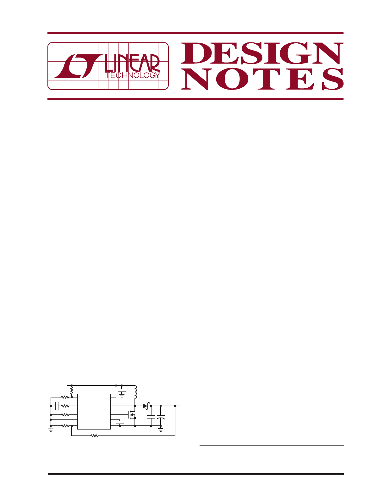
from lower input voltages. A simple boost converter using a Schottky boost diode (Figure 1) is often suffi cient
for low current applications. However, in high current or
space-constrained applications, the power dissipated
by the boost diode can be a problem especially in high
ambient temperature environments. Heat sinks and fans
may be needed to keep the circuit cool, resulting in high
cost and complexity.
To s o l v e t h i s p r o b l e m , t h e S c h o t t k y o u t p u t r e c t i fi e r c a n b e
replaced by a synchronous MOSFET rectifi er (Figure 2).
If MOSFETs with very low R
are used, the power
DS(ON)
dissipation can be reduced to the point where no heat
sinks or active cooling is required, thus reducing costs
and saving space.
Advantages of Synchronous Rectifi cation
Consider the power dissipation o f the single output circuit
in Figure 1. The output diode D1 carries 6.7A of RMS
current to produce 3A of output current from a 5V input.
At this current level, diode D1’s voltage drop is 0.57V,
resulting in 1.6W of power lost as heat. Dissipating 1.6W
in an 85°C (or higher) automotive operating environment
is not trivial. To keep the circuit cool, heat sinks, cooling
fans and multilayer printed circuit boards must be used.
This, of course, adds complexity, cost and size to an
ostensibly simple boost converter.
INPUT*
5V TO 36V
4.7nF
115k
54.9k
1
RUN
12k
2
I
TH
80.6k
4
FREQ
5
MODE/SYNC
12.4k
3
V
FB
FOLLOWS VIN FOR VIN > 24.6V
*V
OUT
LTC1871
229k
SENSE
INTV
GND
V
IN
G
CC
Figure 1. Although This Simple Circuit is Capable of 3A of
Output Current, Beware of Power Dissipation in the Output
Diode D1
22μF
3.3μH
s2
9
10
7
RJK0452
8
6
4.7μF
D1
MBRB2545
22μF
X7R
s4
L1: PULSE PA1494.362
ALL CERAMIC CAPACITORS ARE X7R, TDK
OUTPUT
24V
+
3A
150μF
DN481 F01
A far better solution (featured in a dual output confi guration) is shown in Figure 2, where a synchronous power
MOSFET rectifi er replaces the output diode. Under the
same conditions, th e voltage drop across output synchro nous MOSFET Q2 is only 42mV or 7.4% of the voltage
drop in the diode D1. The resulting power dissipation of
115mW in Q2 is relatively trivial. Another advantage of
using a MOSFET as t he output rectifi er is the elimina tion of
leakage current, about 10mA in the case of the MBR2545
diode—an additional 240mW of power dissipation in the
application of Figure 1.
Dual Output Automotive Boost Converter
Figure 2 illustrates a typical automotive boost application
with a 5V to 36V input voltage range. Here, the converter
produces a 12V output for generic automotive loads
such as entertainment systems, and a 24V output for
circuits such as high power audio amplifi ers. The two
outputs are c ompletely independent and can be con trolled
separately.
Because the circuit in Figure 2 is a boost converter, the
output voltage can be regulated only for input voltages
that are lower than the output voltage. The output voltage regulation versus input voltage is shown in Figure 3.
When the input voltage is higher than the preset output
voltage, synchronous MOSFETs Q2 and Q4 are turned
continuously ON and boost MOSFETs are not switching.
This feature allow s the converter to be used in applica tions
that require boosting only during load transients such as
cold-cranking of a car engine. In this case, the LTC
circuit’s input voltage could be as low as 2.5V.
The effi ciency of this converter (Figure 4) is high enough
that it can be built entirely with surface mount components, requiring no he at sinks. A multilayer PCB with large
c o p p e r a r e a m a y b e s u f fi cient to dissipat e the small amount
of heat resulting from the MOSFETs’ DC resistance, even
at high ambient temperatures.
L, LT, LTC, LTM, Linear Technology and the Linear logo are registered trademarks of
Linear Technology Corporation. All other trademarks are the property of their respective
owners.
Design Note 481
®
3788
08/10/481
15nF
16.9k
V
OUT1
232k
10k
1nF
12.1k
+V
IN
38.3k
12.1k
32313029282726
+
1
SENSE1
2
FREQ
3
PHASMD
4
CHKOUT
5
PLLIN/MODE
6
SGND
7
RUN1
8
RUN2
GND
33910111213141516
10Ω
SENSE1
–
–
SENSE2
1nF
FB1
V
ITH1
SENSE2+V
100pF
0.1μF
SS1
LTC3788
FB2
ITH2
9.09k
LIM
I
100pF
SS2
PGOOD1
PGOOD2
25
SW1
BOOST1
BG1
V
BIAS
PGND
EXTV
INTV
BG2
BOOST
SW2
15nF
TG1
24
23
22
21
20
CC
19
CC
18
17
TG2
12.1k 110k
Figure 2. The LTC3788 Converter is Over 95% Effi cient Even Under Worst-Case Conditions.
When VIN > V
36
34
32
30
28
26
24V OUTPUT
24
22
20
18
OUTPUT VOLTAGE (V)
16
14
12
10
11 13 15
579
17 19 21
INPUT VOLTAGE (V)
, Effi ciency Approaches 100% as Shown in Figure 4
OUT(SET)
12V OUTPUT
23 25 27
29 31 33
35
DN481 F03
Figure 3. The Output Voltage Follows the Input Voltage
when V
IN
> V
OUT(SET)
+V
IN
PA1494.362
0.1μF
BAS140W
V
OUT2
0.1μF
4.7μF
BAS140W
0.1μF
V
OUT2
0.004Ω
0.003Ω
22μF
s2
RJK0452
PA1294.132
RJK0452
99
97
95
93
EFFICIENCY (%)
91
89
87
Q2
RJK0452
22μF
Q1
X7R
s4
Q4
RJK0452
Q3
22μF
0
3
5
4
2
1
+
X7R
s4
7
68
I
(A)
OUT
V
OUT1
24V
3A
150μF
+
DN481 F02
12VIN, 12V
12VIN, 24V
5VIN, 12V
5VIN, 24V
10
9
V
OUT2
12V
8A
150μF
11 12 13
OUT
OUT
OUT
OUT
DN481 F04
Figure 4. The Converter in Figure 2 Peaks at 95%
Effi ciency when Operating from a 5V Input
14
If higher output currents are required, or if lower output
ripple voltage is desired, the two LTC3788 channels can
be combined for a single current-shared output. Simply connect the two outputs and short the respective
FB, ITH, SS and RUN pins. Because the two channels
operate out of phase, output ripple currents are greatly
reduced—nearly canceling out at 50% duty cycle. Thus,
smaller output capacitors can be used with lower output
ripple currents and voltages.
Data Sheet Download
www.linear.com
Linear Technology Corporation
1630 McCarthy Blvd., Milpitas, CA 95035-7417
●
(408) 432-1900
FAX: (408) 434-0507 ● www.linear.com
Conclusion
The LTC3788 dual synchronous boost controller is a
versatile and effi cient solution for demanding automotive
and industrial applications. By minimizing power losses
in the output rectifi er, this converter can be designed
in a very small footprint and operate safely at elevated
ambient temperatures.
For applications help,
call (408) 432-1900, Ext. 3788
dn481f LT/AP 0810 226K • PRINTED IN THE USA
© LINEAR TECHNOLOGY CORPORATION 2010
 Loading...