

L DESIGN FEATURES
C
B
0.1µF
C
F
220pF
L1
0.36µH
C
OUT
470µF
2.5V
×2
C
IN1
330µF
35V
V
IN
5V TO 26V
V
OUT
1.2V
15A
C
VCC
4.7µF
C2
330pF
C1
3.9nF
R
ILIMB
57.6k
R
SET
38.3k
R2
4.7k
R
B
10k
C
OUT
: SANYO 2R5TPD470M5
D
B
: CMDSH4E
L1: IHLP-4040DZ-ER-R36-M11
Q
B
: RJK0301DPB-00-J0
Q
T
: RJK0305DPB-00-J0
R
A
10k
R
SENSE
0.003Ω
R
ILIMT
732Ω
D
B
C
SS
0.01µF
TG Q
T
Q
B
V
IN
LTC3775
SGND
SENSE
I
LIMT
I
LIMB
INTV
CC
SS
BG
PGND
MODE/SYNC
RUN/SHDNCOMP
BOOST
SW
FREQ
FB
+
+
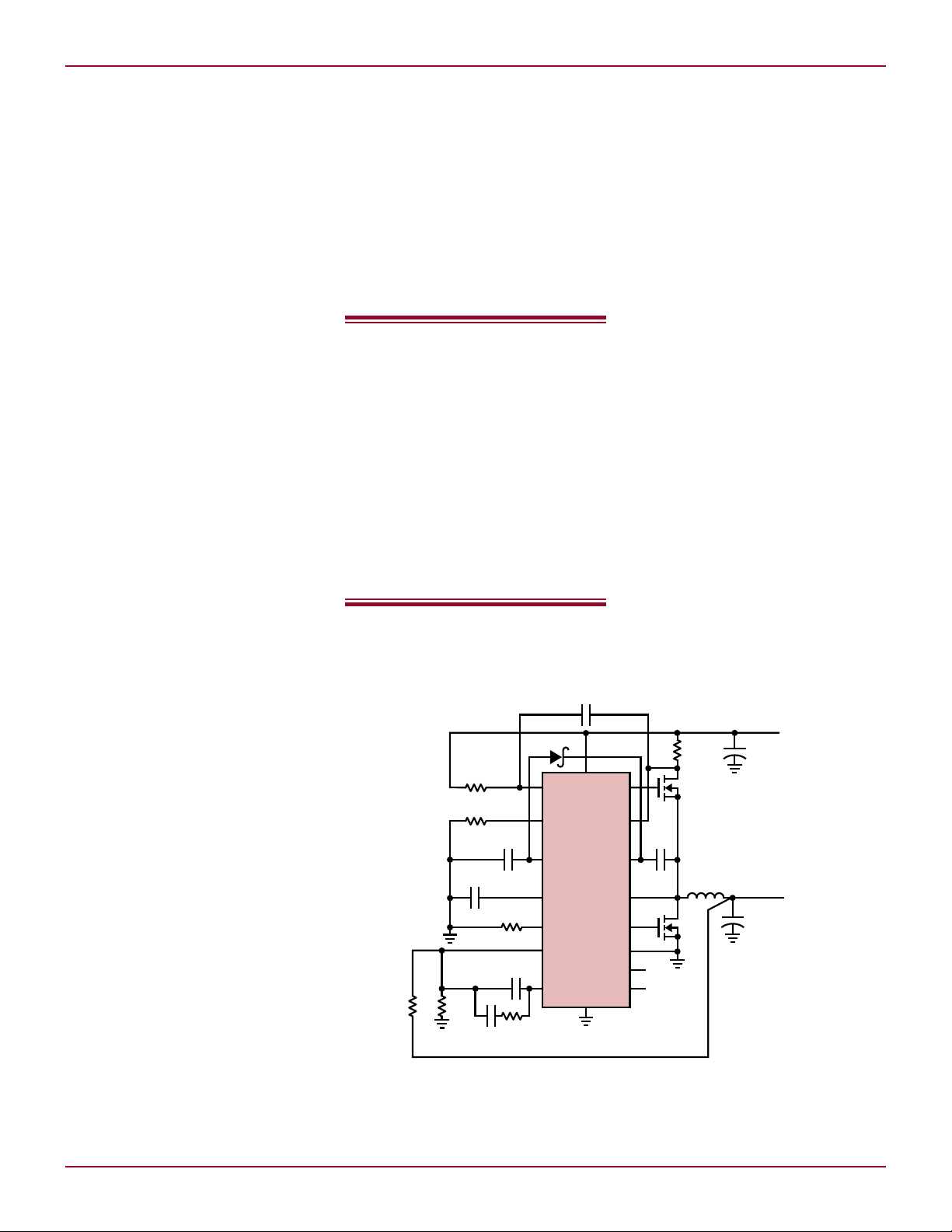
Produce High DC/DC Step-Down
Ratios in Tight Spaces with 30ns
Minimum On-Time Controller in
3mm × 3mm QFN
Introduction
It can be a challenge to design a DC/
DC converter that takes a high voltage
automotive or industrial power supply
down to the 1.5V or lower voltages
required by today’s microprocessors
and programmable logic chips.
To maintain efficiency and performance, designers are often forced to
create a 2-stage solution, which first
steps down to an intermediate voltage
and uses another converter to produce
the low voltage from there. 2-stage
solutions can perform well, and are
handy if the application can use the
intermediate voltage elsewhere, but
2-stage solutions always take more
space and are more costly than a single
stage solution.
Many regulators can produce high
step-down ratios in a single stage if the
switching frequency of the step-down
converter is slowed considerably. However, this option sacrifices efficiency
and requires larger, more expensive
external components, doing little to
solve the space and cost problems
incurred in 2-stage solutions.
The LTC3775 is a voltage mode
DC/DC regulator with a very low
minimum on-time of 30ns, allowing
very wide step-down ratios at high
switching frequencies without sacrificing performance. Unlike most voltage
mode controllers, the LTC3775 offers
cycle-by-cycle programmable current
limit, excellent short circuit protection
and fast transient response over a wide
input voltage range.
A 1.2V Converter Operating
from 5V–28VIN at 350kHz
The LTC3775 is ideal for generating
low output voltages from high input
voltages, a common requirement for
powering CPUs from wide-ranging
20
by Theo Phillips
application providing a continuous
Current mode controllers
are often favored for their
continuous monitoring of
current through the inductor
or switches. While a typical
voltage mode controller
requires additional circuitry
to monitor current in the
power stage, the LTC3775
requires no ancillary
circuits to oversee the entire
switching cycle.
rails such as those found in automotive applications. Figure 1 shows an
Figure 1. A 1.2V, 15A converter
15A from an 5V–26V input.
Current mode controllers are often
favored for their continuous monitoring of current through the inductor or
switches, protecting these components
and the load against short circuits and
pre-biased outputs during start-up.
To avoid these difficulties, a typical
voltage mode controller requires additional circuitry to monitor current in
the power stage. The LTC3775 requires
no ancillary circuits to oversee the
entire switching cycle.
The current limit is programmed
with two resistors (as shown in the
block diagram of Figure 2), corre
sponding to the current measured
through the top and bottom switches
Linear Technology Magazine • December 2009
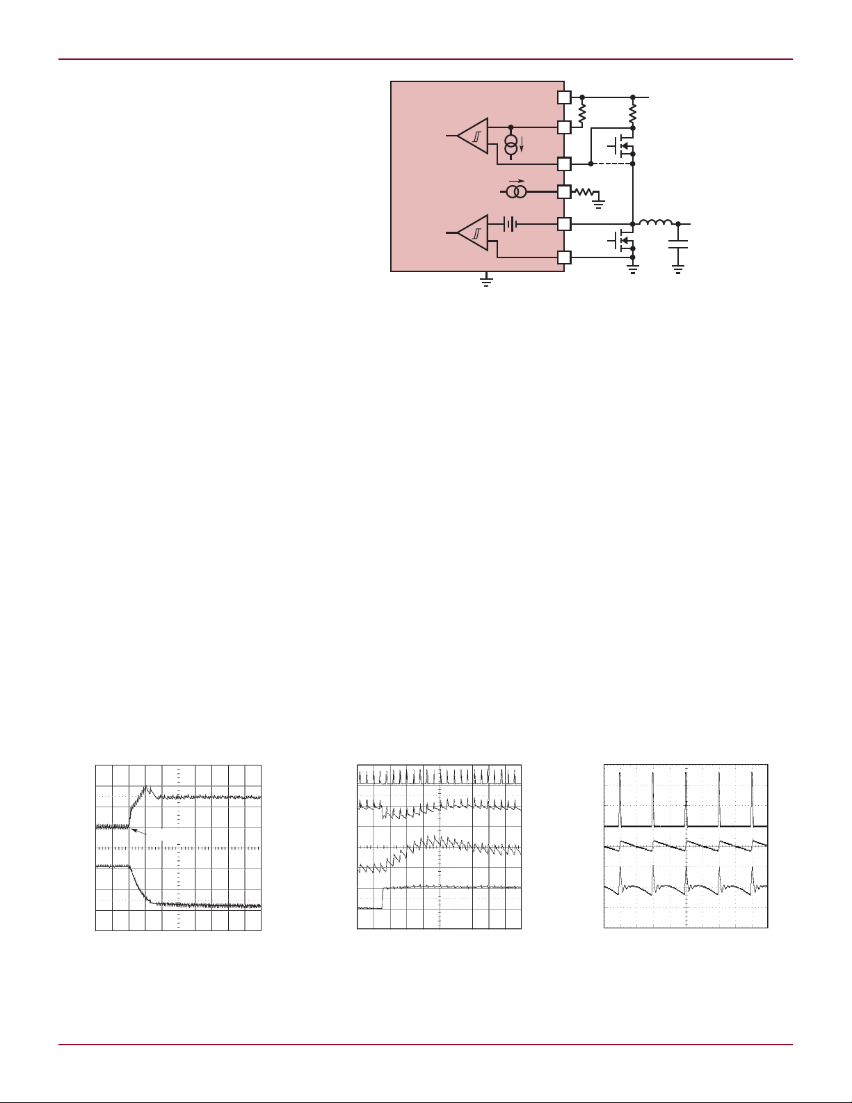
during their respective on times. This
V
OUT(AC)
RIPPLE
20mV/DIV
V
SW
10V/DIV
I
L
10A/DIV
1µs/DIVVIN = 26V
V
OUT
= 1.2V
NO LOAD
R
SET
= 38.3k
V
OUT(AC)
100mV/DIV
V
SW
20V/DIV
I
L
10A/DIV
I
LOAD
10A/DIV
5µs/DIVV
IN
= 12V
V
OUT
= 1.2V
LOAD STEP = 0A TO 10A
MODE/SYNC = 0V
SW FREQ = 500kHz
I
L
20A/DIV
V
SS
1V/DIV
20µs/DIVV
IN
= 12V
V
OUT
= 1.2V
C
SS
= 0.01µF
0A LOAD
+
+
–
100µA
R
ILIMB
(OPT)
10µA
t7
ILIMB
R
ILIMT
7
IN
LTC3775
R
SENSE
SENSE
CTLIM
TURN OFF TG
+
–
CBLIM
EXTEND BG
I
LIMB
SW
I
LIMT
TG Q
T
7
IN
BG Q
B
7
OUT
PGND
SGND
arrangement allows cycle-by-cycle
current limit, regardless of the duty
cycle, and ensures that the inductor
is not saturated.
In a current mode converter, the
voltage on the output of the error
amplifier controls the peak switch
current, such that the switch current
must always be monitored, allowing
the introduction of noise. This may be
most pronounced around 50% duty
cycle in some current mode designs.
Contrast this with a voltage mode
converter, where the error voltage
on V
is compared to a saw-tooth
OUT
ramp, which in turn controls duty
cycle; the larger the error voltage, the
longer the top switch stays on. The
LTC3775 senses current through both
MOSFETs to assure that they do not
exceed programmed limits. During
normal operation, these limits do not
come into play, and noise-free operation is assured.
A high side current limit would be of
little value if the circuit was operated
at its maximum VIN, since the bottom
switch would be on most of the time,
and nothing would protect the synchronous MOSFET. Fortunately, the
low side current limit, programmed by
I
, can limit the current through
LIMB
the bottom switch. Conversely, a fault
at low VIN during the on-time of the
top switch requires a high side current limit for immediate response. The
LTC3775 uses both top- and bottomside current limit circuits to provide
DESIGN FEATURES L
Figure 2. The LTC3775 features high and low side programmable current limits, for cycle-by-cycle
short circuit protection.
optimum protection for the MOSFETs
and inductor.
This current limit approach is effective, as shown by the short circuit
behavior in Figure 3. A hard short
could spell disaster for an unprotected
voltage mode converter. But here, the
inductor does not saturate, and the
input rail maintains its integrity while
the output gracefully drops.
Output voltage is monitored using
an inverting summing amplifier topology, with the FB pin configured as a
virtual ground. The reference voltage
is accurate to within ±0.75% over
temperature. The LTC3775 uses a true
operational error amplifier with 80dB
of open loop gain, and a 25MHz gainbandwidth product. Feedback gain
can be tightly controlled by external
components, allowing the use of “Type
3” compensation, which provides a
phase boost at the LC double pole
frequency and significantly improves
control loop phase margin. Figure 4
shows a characteristically fast load
transient response.
The modulator consists of the
PWM generator, the output MOSFET
drivers and the external MOSFETs
themselves. The modulator gain varies linearly with the input voltage. The
line feedforward circuit compensates
for this change in gain, and provides a
constant gain from the error amplifier
output to the inductor input regardless
of input voltage.
The application in Figure 1 de
mands a minimum on time of just
86ns at the maximum input voltage
of 28V. Many controllers turn the top
gate on at the beginning of the clock
cycle and must wait for the response
time of the PWM comparator before
turning off the top gate. This response
time is typically around 100ns or more.
In addition, those controllers would
make the decision at a noisy interval,
Figure 3. Short circuit behavior for the
converter of Figure 1
Linear Technology Magazine • December 2009
Figure 4. Load transient response for the
converter of Figure 1
Figure 5. The converter of Figure 1
demonstrates a clean switching waveform
with a razor-thin on-time.
21
 Loading...