

advertisement
Triple Output 3-Phase Controller Saves Space and Improves
Performance in High Density Power Converters
Design Note 409
Mike Shriver
Today’s telecommunications, server and network applications require power from a multitude of voltage
rails. Having more than ten rails ranging from 5V to 1V
or less is common. These boards are typically crowded
with heat-producing FPGAs or microprocessors, thus
demanding power converters that are both compact and
highly effi cient. Furthermore, the converters may need
to meet other requirements such as a fast load step
response and rail tracking.
®
The LTC
3773 switching regulator meets and even goes
beyond the above requirements. This device is a 3-phase,
triple output synchronous buck controller with built-in
gate drivers packaged in either a 5mm × 7mm QFN or
a 36-pin SSOP. Its switching frequency can be set to
68.1k
15k
0.01µF
L1:
TDK RLF7030T-2R2M5R4
L2, L3:
TDK RLF7030T-1R5M5R4
C
OUT1 COUT2 COUT3
SANYO POSCAP 4TPE220MF
1nF
8.2k
1nF
5.9k
1nF
10k
10k
0.01µF
20k
,:
POWER DOWN V
POWER DOWN V
POWER DOWN V
0.01µF
20k
150pF
150pF
150pF
31.6k
10Ω
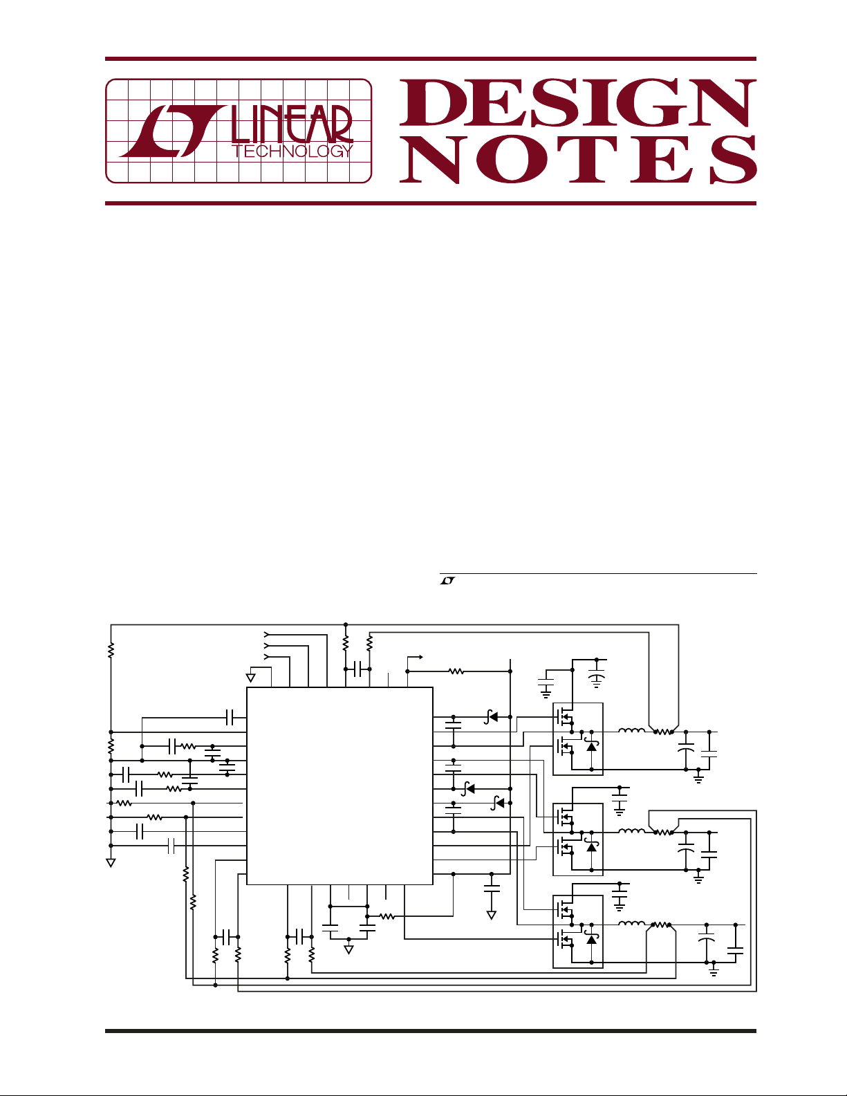
Figure 1. High Density 5A Converter. Total Circuit Size = 1.5in2, with Components on Both Sides
1000pF
OUT1
OUT2
OUT3
37
39
SDB3
PGND
1
TRACK1
2
V
FB1
3
I
TH1
4
SGND
5
I
TH2
6
I
TH3
7
V
FB2
8
V
FB3
9
TRACK2
10
TRACK3
11
12
10Ω
–
–
SENSE2
+
SENSE2
SENSE3
13 14 15 16 17 18 19
1000pF
10Ω
10Ω
1000pF
36
35
–
SDB238SDB1
SENSE1
LTC3773
SENSE3+VCCPLLFLTR
2.2µF
10Ω
34
10Ω
33 32
+
SENSE1
PLLIN/FC
10Ω
0.1µF
PHASEMD
CLKOUT
PGOOD
BOOST1
TG1
SW1
SW2
TG2
BOOST2
BOOST3
TG3
SW3
BG1
BG2
V
BG3
220kHz, 400kHz or 560kHz, or it can be synchronized
to an external clock between 160kHz and 700kHz. The
controller can step down from input voltages as high as
36V and the output voltage can be programmed from
0.6V to 5V.
Figure 1 shows a high density triple output DC/DC converter with each output delivering up to 5A using the
LTC3773 controller. Figure 2 shows the effi ciency of each
ou tp ut ve rsus lo ad cu rr ent ; w here up to 93 % e f fi ci en cy i s
achieved. Reductions in space are realized by the use of
dual channel FETs and a switching frequency of 400kHz
which permits the use of 7mm × 7mm ferrite inductors.
, LT, LTC, LTM and Burst Mode are registered trademarks of Linear Technology
Corporation. All other trademarks are the property of their respective owners.
V
CC
CMDSH-3
0.1µF
0.1µF
CMDSH-3
CMDSH-3
0.1µF
4.7µF
4.5V TO 7V
4.7µF
V
IN
+
4.5V TO 20V
47µF
25V
8 Si4816BDY
1
5
4
8 Si4816BDY
1
5
4
8 Si4816BDY
1
5
4
25V
L1
2.2µH
L2
1.5µH
L3
1.5µH
V
IN
4.7µF
25V
V
IN
4.7µF
25V
7mΩ
7mΩ
7mΩ
C
OUT1
220µF
4V
C
OUT2
220µF
4V
C
OUT3
220µF
4V
+
+
+
22µF
X5R
6, 7
2, 3
6, 7
2, 3
6, 7
2, 3
PGOOD
DR
10k
31
30
29
28
27
26
25
24
23
22
21
20
V
OUT1
3.3V/5A
22µF
X5R
V
OUT2
2.5V/5A
22µF
X5R
V
OUT3
1.8V/5A
DN409 F01
02/15/409
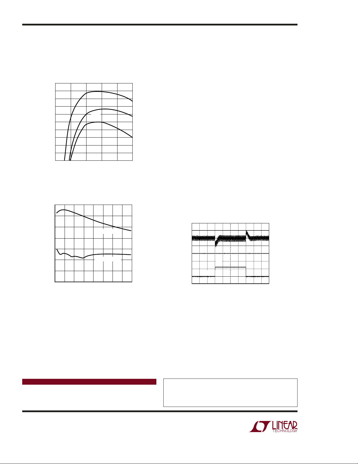
Switching the three rails out of phase results in improved
performance and reduced cost. The use of triple phase
operation instead of single phase can result in a reduc tion
of the input cap acitor ripple current by over 50% as shown
in Figure 3, allowing the use of less input capacitance.
The outputs of two or more phases can be tied together
which results in output ripple current reduction as well
and a faster load step response. Up to six phases can
be synchronized using the CLKOUT pin (on the QFN
part only). Fast and accurate current sharing among the
parallel phases is a result of the LTC3773’s peak current
mode architecture.
94
93
92
91
90
89
88
EFFICIENCY (%)
87
86
85
84
0
123 5
3.3V
2.5V
1.8V
LOAD CURRENT (A)
4
DN409 F02
Figure 2. Effi ciency of the LTC3773 Converter at VIN = 12V,
fSW = 400kHz. One Rail Enabled at a Time
7
6
5
4
3
2
1
0
INPUT CAPACITOR RIPPLE CURRENT (AMPS RMS)
4
81261810 14 20
INPUT VOLTAGE (V)
SINGLE PHASE
TRIPLE PHASE
16
DN409 F03
C o m p e n s a t i o n o f e a c h r a i l i s a c h i e v e d w i t h a n R C n e t w o r k
on the I
pin (error amplifi er output). The external ITH
TH
compensation and the current mode topology allow the
designer to easily stabilize a converter with the minimal
amount of output capacitance using a variety of capacitor types including conduct i v e p o l y m e r , t a n t a l u m a n d
ceramic while still achieving a fast load step response
(see Figure 4).
Other features of the LTC3773 include rail tracking and
sequencing, a PGOOD signal, and three selectable light
load operating modes (continuous conduction mode,
®
Burst Mode
operation and pulse skip mode).
Conclusion
Now designers have a clear and practical solution when
they need a compact and cost effective triple supply
rail requirement in their telecom, server or network
systems.
1.8V
OUT(AC)
50mV/DIV
LOAD STEP
2A/DIV
VIN = 12V
2.5A
5A
50µs/DIV
DN409 F04
Figure 3. Input Capacitor Ripple Current Comparison for
Single Phase and Triple Phase Operation
V
= 3.3V/5A, V
OUT1
Single Phase: φ
Triple Phase: φ
Data Sheet Download
1,2,3
1,2,3
= 2.5V/5A, V
OUT2
= 0º
= 0º,120º, 240º
= 1.8V/5A
OUT3
www.linear.com
Linear Technology Corporation
1630 McCarthy Blvd., Milpitas, CA 95035-7417
●
(408) 432-1900
FAX: (408) 434-0507 ● www.linear.com
Figure 4. 1.8V Load Step Response
For applications help,
call (408) 432-1900, Ext. 2134
dn409f LT/TP 0207 409K • PRINTED IN THE USA
© LINEAR TECHNOLOGY CORPORATION 2006
 Loading...