

DESIGN FEATURES L
GND
0
V
OUT
100V/DIV
I
IN(AVG)
2A/DIV
20ms/DIV
VIN = 24V
C
OUT
= 100µF
2V/DIV
250ns/DIV
GND
CHARGE
CLAMP
V
CC
DONE
FAULT
UVLO1
OVLO1
UVLO2
OVLO2
RDCM
RV
OUT
HVGATE
LVGATE
CSP
CSN
FB
RV
TRANS
T1*
1:10
D1
V
OUT
50V TO 450V
V
TRANS
10V TO 24V
V
CC
TO µP
V
CC
LT3751
GND RBG
R6
40.2k
OFF ON
C3
680µF
C2
2.2µF
s5
C1
10µF
•
•
R7
18.2k
R8
40.2k
M1
R5
6mΩ
1W
D2
+
+
C4
100µF
R9
V
TRANS
R1, 154k
R2, 475k
DANGER HIGH VOLTAGE! OPERATION BY HIGH VOLTAGE TRAINED PERSONNEL ONLY
C5
0.47µF
ALL RESISTORS ARE 0805,
1% RESISTORS UNLESS
OTHERWISE NOTED
D1,D2: VISHAY MURS260
M1: IRF3710Z
T1: WURTH 750310349
LIMIT OUTPUT POWER TO
40W FOR 65°C T1 MAX
AMBIENT OPERATION
*
4.7nF
Y RATED
DC/DC Converter, Capacitor Charger
Takes Inputs from 4.75V to 400V
Introduction
High voltage power supplies and capacitor chargers are readily found in
a number of applications, including
professional photoflashes, security
control systems, pulsed radar systems,
satellite communication systems, and
explosive detonators. The LT3751
makes it possible for a designer to
meet the demanding requirements
of these applications, including high
reliability, relatively low cost, safe
operation, minimal board space and
high performance.
The LT3751 is a general purpose
flyback controller that can be used as
either a voltage regulator or as a capacitor charger. The LT3751 operates in
boundary-mode, between continuous
conduction mode and discontinuous
conduction mode. Boundary-mode
operation allows for a relatively small
transformer and an overall reduced
PCB footprint. Boundary-mode also
reduces large signal stability issues
that could arise from using voltagemode or PWM techniques. Regulation
is achieved with a new dual, overlapping modulation technique using both
by Robert Milliken and Peter Liu
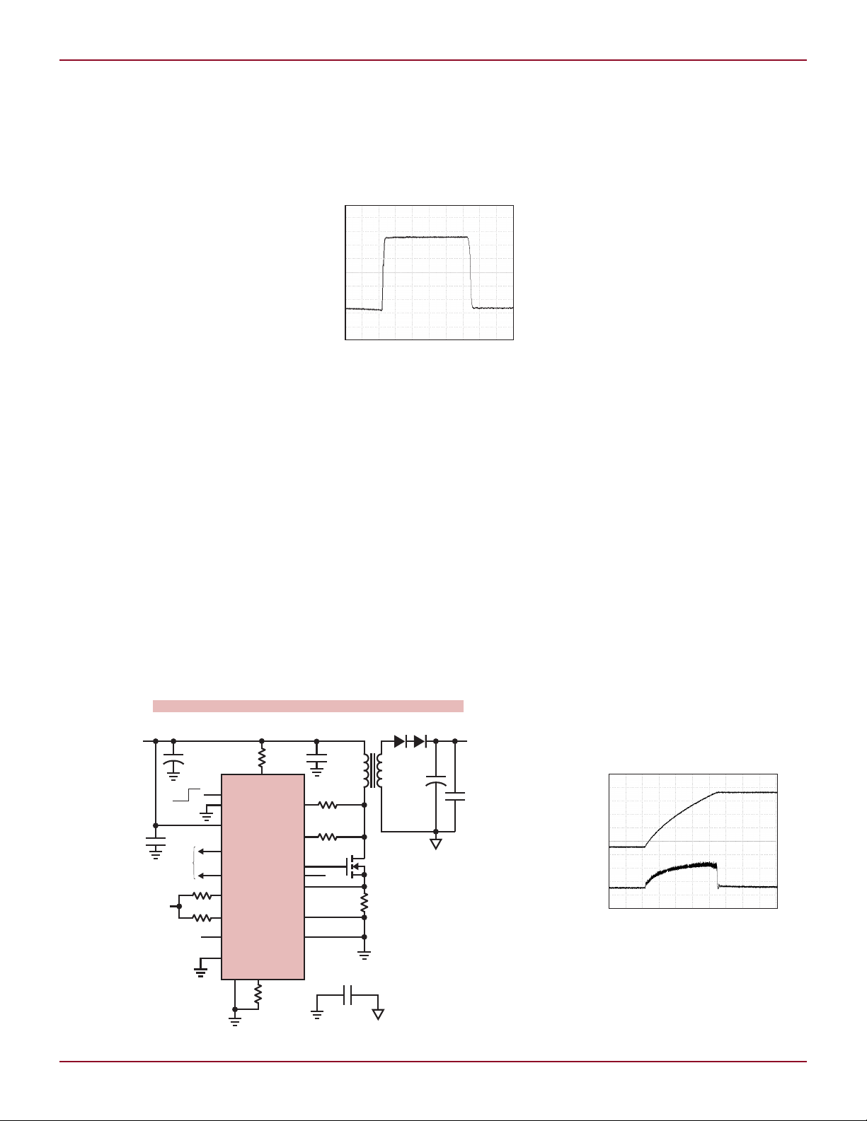
Figure 1. Gate driver waveform
in a typical application
peak primary current modulation and
duty-cycle modulation, drastically reducing audible transformer noise.
The LT3751 features many safety
and reliability functions, including
two sets of undervoltage lockouts
(UVLO), two sets of overvoltage
lockouts (OVLO), no-load operation,
over-temperature lockout (OTLO), internal Zener clamps on all high voltage
pins, and a selectable 5.6V or 10.5V
internal gate driver voltage clamp (no
external components needed). The
LT3751 also adds a start-up/shortcircuit protection circuit to protect
against transformer or external FET
damage. When used as a regulator, the
LT3751’s feedback loop is internally
compensated to ensure stability. The
LT3751 is available in two packages,
either a 20-pin exposed pad QFN or a
20-lead exposed pad TSSOP.
New Gate Driver with Internal
Clamp Requires No External
Components
There are four main concerns when
using a gate driver: output current
drive capability, peak output voltage,
power consumption and propagation
delay. The LT3751 is equipped with a
1.5A push-pull main driver, enough to
drive +80nC gates. An auxiliary 0.5A
PMOS pull-up only driver is also integrated into the LT3751 and is used in
parallel with the main driver for VCC
voltages of 8V and below. This PMOS
driver allows for rail-to-rail operation.
Above 8V, the PMOS driver must be
deactivated by tying its drain to VCC.
Most discrete FETs have a VGS limit
of 20V. Driving the FET higher than
20V could cause a short in the internal gate oxide, causing permanent
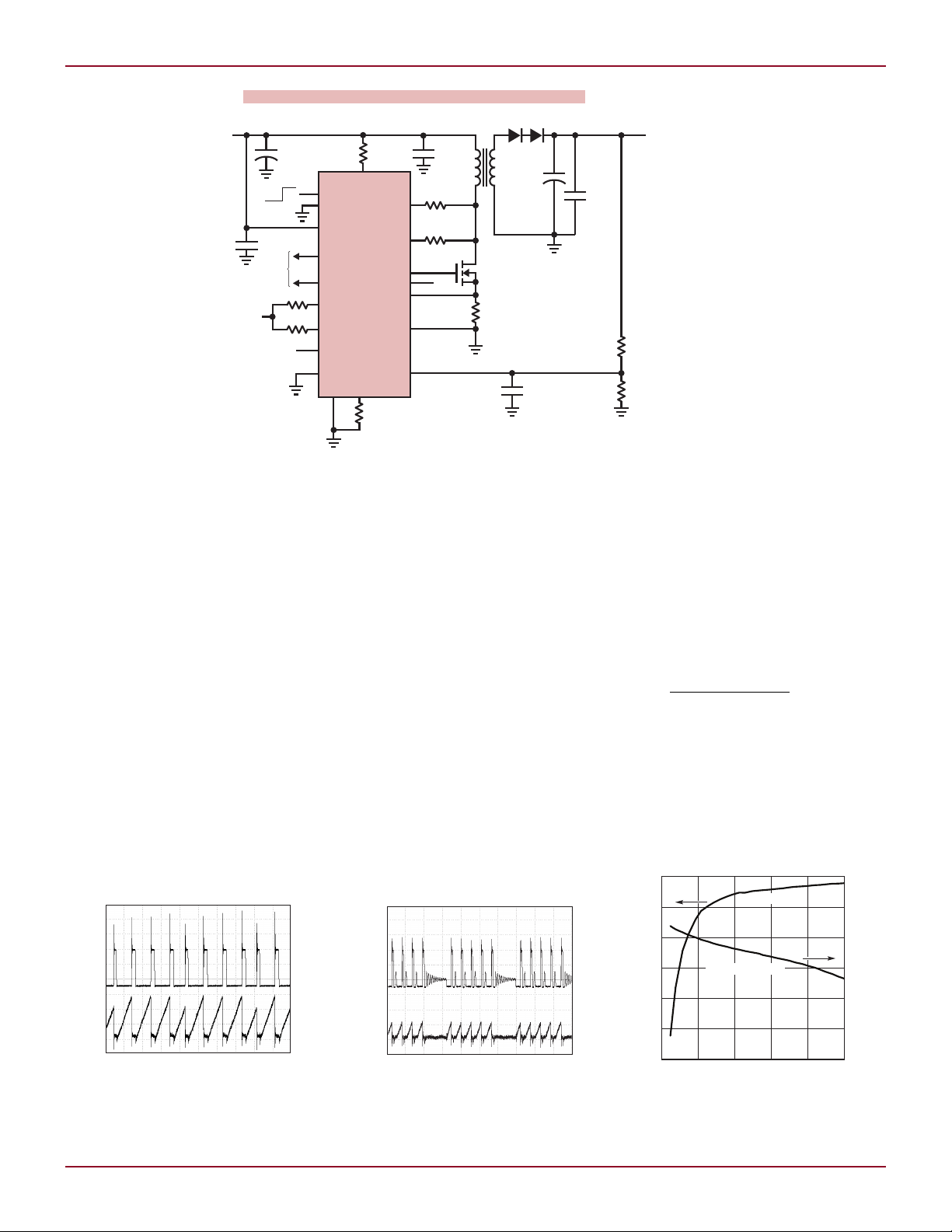
Figure 2. Isolated high voltage capacitor charger from 10V to 24V input
Linear Technology Magazine • March 2009
Figure 3. Isolated high voltage capacitor
charger charging waveform
9
L DESIGN FEATURES
R
N
V V
R
OUT TRIP DIODE
9 8
0 98=•
+
•
.
( )
0
GND
V
DRAIN
20V/DIV
I
PRIMARY
5A/DIV
10µs/DIV
V
OUT
(V)
EFFICIENCY (%)
LOAD CURRENT (mA)
1000
90
60
20 40 60 80
65
70
80
75
85
402
399
400
401
LOAD REGULATION
EFFICIENCY
0
GND
V
DRAIN
20V/DIV
I
PRIMARY
5A/DIV
10µs/DIV
CHARGE
CLAMP
V
CC
DONE
FAULT
UVLO1
OVLO1
UVLO2
OVLO2
RDCM
RV
OUT
HVGATE
LVGATE
CSP
CSN
FB
RV
TRANS
T1**
1:10
D1
V
OUT
400V
V
TRANS
10V TO 24V
V
CC
TO µP
V
CC
LT3751
GND RBG
R6
40.2k
OFF ON
C3
680µF
R10*
499k
R11
1.54k
C2
2.2µF
s5
C1
10µF
•
•
R7
18.2k
R8
40.2k
M1
R5
6mΩ
1W
D2
+
+
C4
100µF
R9
787Ω
V
TRANS
R1,154k
R2, 475k
DANGER HIGH VOLTAGE! OPERATION BY HIGH VOLTAGE TRAINED PERSONNEL ONLY
C5
0.47µF
C6
10nF
ALL RESISTORS ARE 0805,
1% RESISTORS UNLESS
OTHERWISE NOTED
C4: CDE 380LX101M500J042
C5: TDK CKG57NX7R2J474M
D1,D2: VISHAY MURS260
M1: IRF3710Z
T1: WURTH 750310349
USE TWO SERIES 1206,
1% RESISTORS FOR R10
R10: 249k s2
LIMIT OUTPUT POWER TO
40W FOR 65°C T1 MAX
AMBIENT OPERATION
*
**
Figure 4. A 10V to 24V input, 400V regulated power supply
damage. To alleviate this issue, the
LT3751 has an internal, selectable
5.6V or 10.5V gate driver clamp. No
external components are needed, not
even a capacitor. Simply tie the CLAMP
pin to ground for 10.5V operation or
tie to VCC for 5.6V operation. Figure
1 shows the gate driver clamping at
10.5V with a VCC voltage of 24V.
Not only does the internal clamp
protect the FET from damage, it also
reduces the amount of energy injected
into the gate. This increases overall
efficiency and reduces power consumption in the gate driver circuit. The
gate driver overshoot is very minimal,
as seen in Figure 1. Placing the external
FET closer to the LT3751 HVGATE pin
reduces overshoot.
a. Switching waveform for I
10
High Voltage, Isolated
Capacitor Charger from
10V to 24V Input
The LT3751 can be configured as
a fully isolated stand-alone capacitor charger using a new differential
discont inuous-c on duction- mode
(DCM) comparator—used to sense
the boundary-mode condition—and
a new differential output voltage
(V
) comparator. The differential
OUT
operation of the DCM comparator and
V
comparator allow the LT3751 to
OUT
accurately operate from high voltage
input supplies of greater than 400V.
Likewise, the LT3751’s DCM comparator and V
input supplies down to 4.75V. This
accommodates an unmatched range
of power sources.
= 100mA b. Switching waveform for I
OUT
Figure 5. High voltage regulator performance
comparator can work with
OUT
Figure 2 shows a high voltage capacitor charger driven from an input
supply ranging from 10V to 24V. Only
five resistors are needed to operate
the LT3751 as a capacitor charger.
The output voltage trip point can be
continuously adjusted from 50V to
450V by adjusting R9 given by:
The LT3751 stops charging the
output capacitor once the programmed
output voltage trip point (V
reached. The charge cycle is repeated
by toggling the CHARGE pin. The
maximum charge/discharge rate in
= 10mA c. Efficiency and load regulation
OUT
Linear Technology Magazine • March 2009
OUT(TRIP)
) is

DESIGN FEATURES L
P
C FREQUENCY
V V V
AVG
OUT
OUT TRIP RIPPLE
=
• •
•
1
2
2
( )
–
RRIPPLE
W240
(
)
≤
V
CC
R3, 154k
R4, 475k
CHARGE
CLAMP
V
CC
DONE
FAULT
UVLO1
OVLO1
UVLO2
OVLO2
RV
OUT
HVGATE
LVGATE
CSP
CSN
FB
RV
TRANS
T1***
1:3
D1
V
OUT
500V
V
TRANS
100V TO 400V DC
V
CC
10V TO 24V
TO µP
V
CC
LT3751
GND RBG
R6*
625k
OFF ON
C3
100µF
450V
C2
2.2µF
630V
s5
C1
10µF
•
•
R8
137k ×3
R7
88.7k + 7.5k
R10*
208k
R13,20Ω
M1
FQB4N80
R12
68mΩ
1/4W
D2
+
+
C4
220µF
550V
R5
1.11k
V
TRANS
R1**
1.5M
R2**, 9M
DANGER HIGH VOLTAGE! OPERATION BY HIGH VOLTAGE TRAINED PERSONNEL ONLY
C5
0.47µF
630V
RDCM
F1, 1A
R9
66.5k
R11
14.7k +
17.4k
ALL RESISTORS ARE 0805,
1% RESISTORS UNLESS
OTHERWISE NOTED
C4: HITACHI PS22L221MSBPF
C5: TDK CKG57NX7R2J474M
T1: COILCRAFT HA4060-AL
D1,D2: VISHAY US1M
F1: BUSSMANN PCB-1-R
* USE THREE SERIES 1206, 0.1%
RESISTORS FOR R6 & R10
R6: 249k ×2 + 127k
R10: 66.5k ×2 + 75k
** USE TWO SERIES 1206, 1%
RESISTORS FOR R1 & R2
R1: 750k ×2
R2: 4.53M ×2
*** OUTPUT POWER LIMITED TO
20W FOR 65°C T1 AMBIENT
OPERATION
4.7nF
Y RATED
0
V
OUT
AC RIPPLE
10V/DIV
I
IN(AVG)
20mA/DIV
2s/DIV
CHARGE TIME (ms)
V
OUT,TRIP
(V)
INPUT VOLTAGE (V)
400100
530
490
200 300
500
520
510
1000
400
850
550
700
V
OUT,TRIP
CHARGE TIME
the output capacitor is limited by the
temperature rise in the transformer.
Limiting the transformer surface temperature in Figure 2 to 65°C with no
air flow requires the average output
power to be ≤40W given by:
where V
voltage, V
OUT(TRIP)
is the output trip
is the ripple voltage
RIPPLE
on the output node, and frequency is
the charge/discharge frequency. Two
techniques are used to increase the
available output power: increase the
airflow across the transformer, or increase the size of the transformer itself.
Figure 3 shows the charging waveform
and average input current for a 100µF
output capacitor charged to 400V in
less than 100ms (R9 = 976Ω).
For output voltages higher than
450V, the transformer in Figure 2 must
be replaced with one having higher
primary inductance and a higher
turns ratio. Consult the LT3751 data
Figure 6. The LT3751 protecting the
output during a no-load condition
sheet for proper transformer design
procedures.
High Voltage Regulated Power
Supply from 10V to 24V Input
The LT3751 can also be used to convert
a low voltage supply to a much higher
voltage. Placing a resistor divider from
the output node to the FB pin and
ground causes the LT3751 to operate as a voltage regulator. Figure 4
shows a 400V regulated power supply
operating from an input supply range
of 10V to 24V.
The LT3751 uses a regulation control scheme that drastically reduces
audible noise in the transformer and
the input and output ceramic bulk
capacitors. This is achieved by using
an internal 26kHz clock to synchronize
the primary winding switch cycles.
Within the clock period, the LT3751
modulates both the peak primary
current and the number of switching cycles. Figures 5a and 5b show
heavy-load and light-load waveforms,
respectively, while Figure 5c shows
efficiency over most of the operating
range for the application in Figure 4.
The clock forces at least one switch
cycle every period which would overcharge the output capacitor during a
no-load condition. The LT3751 handles no-load conditions and protects
against over-charging the output node.
Figure 6 shows the LT3751 protecting
during a no-load condition.
Resistors can be added to RV
OUT
and
RBG to add a second layer of protection, or they can be omitted to reduce
component count by tying RV
OUT
and
RBG to ground. The trip level for the
V
comparator is typically set 20%
OUT
higher than the nominal regulation
voltage. If the resistor divider were to
fail, the V
comparator would disable
OUT
switching when the output climbed to
20% above nominal.
Linear Technology Magazine • March 2009
Figure 7. A 100V to 400V input, 500V output, isolated capacitor charger
Figure 8. Isolated capacitor charger V
and charge time with respect to input voltage
OUT(TRIP)
11

L DESIGN FEATURES
OUTPUT VOLTAGE (V)
INPUT VOLTAGE (V)
400100
398
395
200 300
396
397
I
OUT
= 10mA
I
OUT
= 25mA
I
OUT
= 50mA
EFFICIENCY (%)
OUTPUT CURRENT (mA)
750
90
40
50
25 50
60
70
80
VIN = 100V
VIN = 250V
VIN = 400V
V
CC
R3, 154k
R4, 475k
CHARGE
CLAMP
V
CC
DONE
FAULT
UVLO1
OVLO1
UVLO2
OVLO2
RV
OUT
HVGATE
LVGATE
CSP
CSN
FB
RV
TRANS
T1***
1:3
D1
V
OUT
400V
V
TRANS
100V TO 400V DC
V
CC
10V TO 24V
TO µP
V
CC
LT3751
GND RBG
R6*
615k
OFF ON
C3
100µF
C2
2.2µF
s5
C1
10µF
C6
10nF
•
•
R8*
411k
R13,20Ω
M1
FQB4N80
R10
68mΩ
¼W
D2
+
+
C4
100µF
R12
1.54k
R11**
499k
V
TRANS
R1**, 1.5M
R2**, 9M
DANGER HIGH VOLTAGE! OPERATION BY HIGH VOLTAGE TRAINED PERSONNEL ONLY
C5
0.47µF
RDCM
F1, 1A
R9
66.5k
ALL RESISTORS ARE 0805,
1% RESISTORS UNLESS
OTHERWISE NOTED
C4: CDE 380LX101M500J042
C5: TDK CKG57NX7R2J474M
T1: COILCRAFT HA4060-AL
D1,D2: VISHAY US1M
F1: BUSSMANN PCB-1-R
* USE THREE SERIES 1206, 1%
RESISTORS FOR R6 & R8
R6: 205k ×3
R8: 137k ×3
** USE TWO SERIES 1206, 1%
RESISTORS FOR R1, R2 & R11
R1: 750k ×2
R2: 4.53M ×2
R11: 249k ×2
*** OUTPUT POWER LIMITED TO
20W FOR 65°C T1 AMBIENT
OPERATION
R7
95.3k
can also be used for a capacitor
charger. The LT3751 operates as a
capacitor charger until the FB pin
reaches 1.225V, after which the
LT3751 operates as a voltage regulator.
This keeps the capacitor topped-off
until the application needs to use its
energy. The output resistor divider
forms a leakage path from the output
capacitor to ground. When the output
voltage droops, the LT3751 feedback
circuit will keep the capacitor topped-
12
Figure 9. A 100V to 400V input, 400V output, capacitor charger and voltage regulator
Note that the FB pin of the LT3751
a. Overall efficiency b. Line regulation
Figure 10. High voltage input and output regulator performance
off with small, low current bursts of
charge as shown in Figure 6.
High Input Supply Voltage,
Isolated Capacitor Charger
As mentioned above, the LT3751 differential DCM and V
allow the part to accurately work from
very high input supply voltages. An
offline capacitor charger, shown in
Figure 7, can operate with DC input
voltages from 100V to 400V. The transformer provides galvanic isolation from
comparators
OUT
the input supply to output node—no
additional magnetics required.
Input voltages greater than 80V
require the use of resistor dividers
on the DCM and V
comparators
OUT
(charger mode only). The accuracy of
the V
trip threshold is heightened
OUT
by increasing current IQ through R10
and R11; however, the ratio of R6/R7
should closely match R10/R11 with
tolerances approaching 0.1%. A trick
is to use resistor arrays to yield the
desired ratio. Achieving 0.1% ratio accuracy is not difficult and can reduce
the overall cost compared to using
individual 0.1% surface mount resistors. Note that the absolute value of
the individual resistors is not critical,
only the ratio of R6/R7 and R10/R11.
The DCM comparator is less critical
and can tolerate resistance variations
greater than 1%.
The 100V to 400VDC input capacitor charger has an overall V
accuracy of better than 6% over the
entire operating range using 0.1% resistor dividers. Figure 8 shows a typical
performance for V
OUT(TRIP)
and charge
time for the circuit in Figure 7.
Linear Technology Magazine • March 2009
OUT(TRIP)

DESIGN FEATURES L
V
TRANS
100V TO 200V DC
V
CC
V
CC
R11, 84.5k
R12, 442k
UVLO1
OVLO1
UVLO2
OVLO2
DONE
FAULT
CHARGE
CLAMP
V
CC
HVGATE
LVGATE
CSP
CSN
FB
RV
TRANS
TO µP
V
CC
LT3751
LT4430
GND RBG
R3
210k
OFF ON
C3
22µF
350V
s2
C2
1µF
C1
100pF
C4
1µF
250V
s2
C7
400µF
330V
C8
22nF
R17
3.16k
R14
249k
V
OUT
282V
225mA
C6
0.1µF
630V
ISOLATION
BOUNDARY
C5
0.01µF
630V
C9
3.3µF
C10
0.47µF
•
M2
M1
D1
R8
2.49k
R7
475Ω
R18
274Ω
R6
40mΩ
1/4W
V
TRANS
R9, 2.7M
R5, 210k
R13
5.11Ω
R16, 1k
R10, 4.3M
DANGER HIGH VOLTAGE! OPERATION BY HIGH VOLTAGE TRAINED PERSONNEL ONLY
RDCM
RV
OUT
U1
ALL RESISTORS ARE 0805,1% RESISTORS
UNLESS OTHERWISE NOTED
C7: 330FK400M22X38
D1: 12V ZENER
D2: MURS140
D3: P6kE200A
D4, D5: STTH112A
D6: BAT54
D7: BAS516
M1: IRF830
M2: STB11NM60FD
T1: TDK SRW24LQ-UxxH015
(Np:Ns:Npb:Nsb=1:2:0.08:0.08)
U1: PS2801-1
U2: LT4430
R4, 105k
R2, 10ΩD2
D3
D5
D6
D4
Np
Ns
Nsb
U2
VINCOMP
GND
OC FB
OPTO
Npb
T1
D7
R15
221k
R1
49.9k
1/2W
•
•
•
+
+
1
1 1 1
1
11
1
1
1
2
2
2
2
2
2
2
F1, 2A
1 2
4.7nF
Y RATED
0
GND
V
DRAIN
100V/DIV
I
PRIMARY
2A/DIV
20µs/DIV
0
GND
V
DRAIN
100V/DIV
I
PRIMARY
2A/DIV
20µs/DIV
R
V
A
OUT TRIP
11
1 225
50
=
−
( )
.
µ
Figure 11. Fully isolated, high output voltage regulator
High Input Supply Voltage,
Non-Isolated Capacitor
Charger/Regulator
The FB pin of the LT3751 can also
be configured for charging a capacitor from a high input supply voltage.
Simply tie a resistor divider from the
output node to the FB pin. The resistor dividers on the R
pins can tolerate 5% resistors, and all
the R
removed. This lowers the number and
and RBG pin resistors are
V(OUT)
the tolerance of required components,
reducing board real estate and overall
design costs. With the output voltage
resistor divider, the circuit in Figure
9 is also a fully functional, high-ef
ficiency voltage regulator with load
Linear Technology Magazine • March 2009
VTRANS
a. I
and R
= 225mA b. I
OUT
DCM
-
and line regulation better than 1%.
Efficiency and line regulation for the
circuit in Figure 9 are shown in Figure
10a and Figure 10b, respectively.
Alternatively, a resistor can be tied
from V
pin. This mimics the V
to the OVLO1 pin or OVLO2
OUT
compara-
OUT
tor, stopping charging once the target
voltage is reached. The FB pin is tied
to ground. The CHARGE pin must be
toggled to initiate another charge sequence, thus the LT3751 operates as
a capacitor charger only. Resistor R12
is omitted from Figure 9 and resistor
R11 is tied from V
or OVLO2. R11 is calculated using the
following equation:
Figure 12. Switching waveforms
OUT
directly to OVLO1
Note that OVLO1 or OVLO2 will
cause the FAULT pin to indicate a
fault when the target outpaut voltage,
V
OUT(TRIP) ,
is reached.
High Voltage Input/Output
Regulator with Isolation
Using a resistor divider from the output
node to the FB pin allows regulation
but does not provide galvanic isolation.
Two auxiliary windings are added to
the transformer in circuit shown in
Figure 11 to drive the FB pin, the
OUT
= 7.1mA
continued on page 42
13

L NEW DEVICE CAMEOS
EFFICIENCY (%)
INPUT DC VOLTAGE (V)
200100
100
70
120 140 160 180
75
80
90
85
95
P
OUT
= 63W
P
OUT
= 48W
P
OUT
= 25W
OUTPUT VOLTAGE ERROR (V)
I
OUT
(mA)
2500
–0.5
–0.25
0
0.25
0.5
10050 150 200
battery whether external or internal.
Programming the charge current only
requires a single external resistor.
The fault management system of the
LTC4012 family suspends charging
immediately for various conditions.
First is battery overvoltage protection,
which can occur with the sudden loss
of battery load during bulk charge.
Second, each IC features internal
over-temperature protection to prevent silicon damage during elevated
thermal operation.
The LTC4012 family has a logic-level
shutdown control input and three
open-drain status outputs. First is an
input current limit (ICL) status flag to
tell the system when VIN is running at
over 95% of its current capacity. The
input current limit accuracy is typically ±3% and a maximum of ±4% over
the full operating temperature range.
Next is the AC present status, which
indicates when VIN is within a valid
range for charging under all modes of
operation. The last is a charge status
output can indicate bulk or C/10
charge states. The control input and
status outputs of the LTC4012, along
with the analog current monitor output, can be used by the host system
to perform necessary preconditioning,
charge termination and safety timing
functions.
4MHz Synchronous StepDown DC/DC Converter
Delivers up to 1.25A from a
3mm × 3mm DFN
The LTC3565 is a high efficiency synchronous step-down regulator that
can deliver up to 1.25A of continuous
output current from a 3mm × 3mm
DFN (or MSOP-10E) package. Using
a constant frequency of (up to 4MHz)
and current mode architecture, the
LTC3565 operates from an input voltage range of 2.5V to 5.5V making it
ideal for single cell Li-Ion, or multicell
Alkaline/NiCad/NiMH applications.
It can generate output voltages as
low as 0.6V, enabling it to power the
latest generation of low voltage DSPs
and microcontrollers. An independent
RUN pin enables simple turn-on and
shutdown. Its switching frequency
is user programmable from 400kHz
to 4MHz, enabling the designer to
optimize efficiency while avoiding critical noise-sensitive frequency bands.
The combination of its 3mm × 3mm
DFN-10 (or MSOP-10) package and
high switching frequency keeps external inductors and capacitors small,
providing a very compact, thermally
efficient footprint.
The LTC3565 uses internal switches
with an R
of only 0.13Ω (N-Chan-
DS(ON)
nel lower FET) and 0.15Ω (P-Channel
upper FET) to deliver efficiencies
as high as 95%. It also utilizes low
dropout 100% duty cycle operation
to allow output voltages equal to VIN,
further extending battery run time.
The LTC3565 utilizes Automatic Low
Ripple ( < 25mV
) Burst Mode®
P–P
operation to offer only 40µA no load
quiescent current. If the application is
noise sensitive, Burst Mode operation
can be disabled using a lower noise
pulse-skipping mode, which still offers
only 330µA of quiescent current. The
LTC3565 can be synchronized to an
external clock throughout its entire
frequency range. Other features include ±2% output voltage accuracy and
over-temperature protection.
L
LT3751, continued from page 13
LT3751 controller, and the optocoupler
on the feedback resistor divider. The
auxiliary windings provide the desired
galvanic isolation boundary while
maintaining an isolated feedback path
from the output node to the LT3751
FB pin. Figures 12 and 13 show the
regulator’s performance.
The fully isolated, high voltage input/output regulator yields over 90%
efficiency. Load regulation is excellent
as shown in Figure 13b, due mainly
to the added gain of the optocoupler
circuit.
Conclusion
The ability to run from any input
supply voltage ranging from 4.75V
to greater than 400V and the abundance of safety features make the
LT3751 an excellent choice for high
voltage capacitor chargers or high
voltage regulated power supplies. In
fact, the LT3751 is, for now, the only
42
42
a. Efficiency b. Load regulation
Figure 13. Fully isolated, high voltage regulator performance
boundary-mode capacitor charger
controller that can accurately operate
from extremely high input voltages.
The LT3751 simplifies design by integrating many functions that—due
to cost and board real-estate—would
otherwise not be realizable. Although
LT3751 includes many more features
than we can show in one article. We
recommended consulting the data
sheet or calling the Linear Technology
applications engineering department
for more in-depth coverage of all available features.
L
several designs are shown here, the
Linear Technology Magazine • March 2009
 Loading...