

FEATURES
LTC3733/LTC3733-1
3-Phase, Buck
Controllers for AMD CPUs
U
DESCRIPTIO
■
3-Phase Controller with Onboard MOSFET Drivers
■
Current Mode Control Ensures Current Sharing
■
Differential Amplifier Accurately Senses V
■
±5% Output Current Matching Optimizes Thermal
OUT
Performance and Size of Inductors and MOSFETs
■
Reduced Input and Output Capacitance
■
Supports Active Voltage Positioning
■
VID Programmable Output Voltage from 0.8V to 1.55V
(AMD OpteronTM CPU)
■
6-Phase, 90A to 120A Operation
■
Output Power Good Indicator with Adaptive Blanking
■
210kHz to 530kHz Per Phase, PLL, Fixed Frequency
■
Synchronizable (LTC3733-1)
■
PWM, Stage Shedding or Burst Mode® Operation
■
OPTI-LOOP® Compensation Minimizes C
■
Adjustable Soft-Start Current Ramping
■
Short-Circuit Shutdown Timer with Defeat Option
■
No_CPU Detection
■
36-Lead 0.209" SSOP and 38-Lead (5mm × 7mm) QFN
OUT
U
APPLICATIO S
■
High Performance Notebook Computers
■
Servers, Desktop Computers and Workstations
The LTC®3733 family are PolyPhase® synchronous stepdown switching regulator controllers that drive all
N-channel external power MOSFET stages in a phaselockable, fixed frequency architecture. The 3-phase controller drives its output stages with 120° phase separation
at frequencies of up to 530kHz per phase to minimize the
RMS current dissipated by the ESR of both the input and
output filter capacitors. The 3-phase technique effectively
triples the fundamental frequency, improving transient
response while operating each phase at an optimal frequency for efficiency and ease of thermal design. Light
load efficiency is optimized by using a choice of output
stage shedding or Burst Mode technology.
A differential amplifier provides true remote sensing of both
the high and low sides of the output voltage at load points.
Soft-start and a defeatable, timed short-circuit shutdown
protect the MOSFETs and the load. A foldback current
circuit also provides protection for the external MOSFETs
under short-circuit or overload conditions. An all-“1” VID
detector turns off the regulator after 1µs timeout.
, LTC and LT are registered trademarks of Linear Technology Corporation.
Burst Mode, OPTI-LOOP and PolyPhase are registered trademarks of Linear Technology
Corporation. AMD Opteron is a trademark of Advanced Micro Devices, Inc.
TYPICAL APPLICATIO
5V
POWER GOOD INDICATOR
OPTIONAL SYN IN
U
CC
10µF
0.1µF
SW3 SW2 SW1
5 VID BITS
ON/OFF
5k
680pF
0.1µF
100pF
LTC3733-1
BOOST1
BOOST2
BOOST3
PGOOD
PLLIN
PLLFLTR
VID0-VID4
RUN
I
TH
SS
SGND
EAIN
–
IN
+
IN
Figure 1. High Current Triple Phase Step-Down Converter
SW1
SENSE1
SENSE1
SW2
PGND
SENSE2
SENSE2
SW3
SENSE3
SENSE3
TG1V
BG1
TG2
BG2
TG3
BG3
L1 0.8µH
+
–
V
IN
L2 0.8µH
+
–
V
IN
L3 0.8µH
+
–
0.002Ω
D1
0.002Ω
D2
0.002Ω
D3
+
+
22µF
35V
×2
V
OUT
0.8V TO 1.55V
65A
C
OUT
470µF
4V
×4
3733 F01
V
IN
5V TO 28V
3733f
1
LTC3733/LTC3733-1
WWWU
ABSOLUTE AXI U RATI GS
(Note 1)
Topside Driver Voltages (BOOSTN)............38V to –0.3V
Switch Voltage (SWN)...................................32V to –5V
Boosted Driver Voltage (BOOSTN – SWN)....7V to –0.3V
Peak Output Current <1ms (TGN, BGN) ..................... 5A
Supply Voltage (VCC), PGOOD
Pin Voltages ................................................7V to –0.3V
PLLIN, RUN, SS,
PLLFLTR, FCB Voltages ............................. VCC to –0.3V
UU
W
PACKAGE/ORDER I FOR ATIO
VID1
RUN
PLLFLTR
FCB
DIFFOUT
EAIN
SGND
SENSE1
SENSE1
SENSE2
SENSE2
SENSE3
SENSE3
VID2
TOP VIEW
1
2
3
4
+
5
IN
–
6
IN
7
8
9
+
10
–
11
+
12
–
13
–
14
+
15
16
SS
17
I
TH
18
G PACKAGE
36-LEAD PLASTIC SSOP
T
= 125°C, θJA = 95°C/W
JMAX
36
35
34
33
32
31
30
29
28
27
26
25
24
23
22
21
20
19
VID0
PGOOD
BOOST1
TG1
SW1
BOOST2
TG2
SW2
V
CC
BG1
PGND
BG2
BG3
SW3
TG3
BOOST3
VID4
VID3
ORDER PART
NUMBER
LTC3733CG
ITH Voltage................................................2.4V to –0.3V
Operating Ambient Temperature Range....... 0°C to 70°C
Junction Temperature (Note 2).............................125°C
Storage Temperature Range
LTC3733CG .......................................–65°C to 150°C
LTC3733CUHF-1 ...............................–65°C to 125°C
Lead Temperature (LTC3733CG)
(Soldering, 10 sec) ...............................................300°C
TOP VIEW
ORDER PART
NUMBER
PLLIN
RUN
VID1
VID0
PGOOD
BOOST1
TG1
38 37 36 35 34 33 32
SW1
VID4
31
30
29
28
27
26
25
24
23
22
21
20
BOOST3
BOOST2
TG2
SW2
V
CC
DRV
BG1
PGND
BG2
BG3
SW3
TG3
1PLLFLTR
FCB
2
+
IN
3
–
IN
4
DIFFOUT
SENSE1
SENSE1
SENSE2
SENSE2
SENSE3
EXPOSED PAD IS SGND (PIN 39) MUST BE SOLDERED TO PCB
5
EAIN
6
SGND
7
+
8
–
9
+
10
–
11
–
12
13 14 15 16
+
TH
SS
I
SENSE3
38-LEAD (7mm × 5mm) PLASTIC QFN
UHF PACKAGE
T
= 125°C, θJA = 34°C/W
JMAX
39
VID2
17 18 19
VID3
LTC3733CUHF-1
CC
UHF PART
MARKING
37331
Consult LTC Marketing for parts specified with wider operating temperature ranges.
ELECTRICAL CHARACTERISTICS
temperature range, otherwise specifications are at TA = 25°C. VCC = V
The ● denotes the specifications which apply over the full operating
= VSS = 5V unless otherwise noted.
RUN
SYMBOL PARAMETER CONDITIONS MIN TYP MAX UNITS
Main Control Loop
V
REGULATED
V
SENSEMAX
I
MATCH
Regulated Voltage at IN
Maximum Current Sense Threshold V
Current Match Worst-Case Error at V
+
(Note 3); VID Code = 10011, V
= 0.5V, V
EAIN
V
SENSE1–, VSENSE2–, VSENSE3–
Open, 65 75 85 mV
ITH
SENSE(MAX)
= 1.2V 1.067 1.075 1.083 V
ITH
● 1.064 1.075 1.086 V
= 0.8V, 1.55V ● 62 75 88 mV
–5 5 %
3733f
2
LTC3733/LTC3733-1
ELECTRICAL CHARACTERISTICS
temperature range, otherwise specifications are at TA = 25°C. VCC = V
The ● denotes the specifications which apply over the full operating
= VSS = 5V unless otherwise noted.
RUN
SYMBOL PARAMETER CONDITIONS MIN TYP MAX UNITS
V
LOADREG
V
REFLNREG
g
m
g
mOL
V
FCB
I
FCB
V
BINHIBIT
Output Voltage Load Regulation (Note 3)
Measured in Servo Loop, ∆I
Measured in Servo Loop, ∆I
Voltage = 1.2V to 0.7V ● 0.1 0.5 %
TH
Voltage = 1.2V to 2V ● –0.1 –0.5 %
TH
Output Voltage Line Regulation VCC = 4.5V to 7V 0.03 %/V
Transconductance Amplifier g
m
ITH = 1.2V, Sink/Source 25µA (Note 3) 2.5 3.05 3.6 mmho
Transconductance Amplifier GBW ITH = 1.2V, (gm • ZL, ZL = Series 1k-100kΩ-1nF) 1.5 MHz
Forced Continuous Threshold ● 0.58 0.60 0.62 V
FCB Bias Current V
Burst Inhibit Threshold Measured at FCB pin VCC – 1.5 V
= 0.65V 0.2 0.7 µA
FCB
– 0.7 V
CC
– 0.3 V
CC
UVR Undervoltage SS Reset VCC Lowered Until the SS Pin is Pulled Low 3.3 3.8 4.5 V
I
Q
V
RUN
I
SS
V
SSARM
Input DC Supply Current (Note 4)
Normal Mode V
Shutdown V
RUN Pin ON Threshold V
Soft-Start Charge Current V
= 5V 2.5 mA
CC
= 0V, VID0 to VID4 Open 20 100 µA
RUN
, Ramping Positive 1 1.5 1.9 V
RUN
= 1.9V –0.8 –1.5 –2.5 µA
SS
SS Pin Arming Threshold VSS, Ramping Positive Until Short-Circuit 3.8 4.5 V
Latch-Off is Armed
V
SSLO
I
SCL
I
SDLHO
I
SENSE
SS Pin Latch-Off Threshold VSS, Ramping Negative 3.3 V
SS Discharge Current Soft-Short Condition V
Shutdown Latch Disable Current V
= 0.375V, VSS = 4.5V 1.5 5 µA
EAIN
= 0.375V, V
EAIN
= 4.5V –5 –1.5 µA
SS
SENSE Pins Source Current SENSE1+, SENSE1–, SENSE2+, SENSE2–,1320µA
SENSE3+, SENSE3– All Equal 1.2V; Current at Each Pin
DF
MAX
TG tR,t
BG t
R, tF
TG/BG t
F
Maximum Duty Factor In Dropout 95 98.5 %
Top Gate Rise Time C
Top Gate Fall Time C
Bottom Gate Rise Time C
Bottom Gate Fall Time C
Top Gate Off to Bottom Gate On Delay All Controllers, C
1D
= 3300pF 30 90 ns
LOAD
= 3300pF 40 90 ns
LOAD
= 3300pF 30 90 ns
LOAD
= 3300pF 20 90 ns
LOAD
= 3300pF Each Driver 60 ns
LOAD
Synchronous Switch-On Delay Time
BG/TG t
Bottom Gate Off to Top Gate On Delay All Controllers, C
2D
= 3300pF Each Driver 60 ns
LOAD
Top Switch-On Delay Time
t
ON(MIN)
Minimum On-Time Tested with a Square Wave (Note 5) 120 ns
VID Parameters
VID
VID
VID
IL
IH
PULLUP
Maximum Low Level Input Voltage 0.8 V
Minimum High Level Input Voltage 2 V
VID0 to VID4 Internal Pull-Up 150 kΩ
Resistance
ATTEN
ERR
VID0 to VID4 (Note 6) ● –0.25 0.25 %
Power Good Output Indication
V
PGL
I
PGOOD
V
PGTHNEG
V
PGTHPOS
t
PGBLNK
PGOOD Voltage Output Low I
PGOOD Output Leakage V
PGOOD Trip Thesholds V
V
Ramping Negative VID Code = 10011 –7 –10 –14 %
DIFFOUT
V
Ramping Positive PGOOD Goes Low After V
DIFFOUT
= 2mA 0.1 0.3 V
PGOOD
= 5V ±1 µA
PGOOD
with Respect to Set Output Voltage,
DIFFOUT
Delay 7 10 14 %
UVDLY
Power Good Blanking After VID Changes Outside PGOOD Window 120 µs
3733f
3
LTC3733/LTC3733-1
ELECTRICAL CHARACTERISTICS
temperature range, otherwise specifications are at TA = 25°C. VCC = V
The ● denotes the specifications which apply over the full operating
= VSS = 5V unless otherwise noted.
RUN
SYMBOL PARAMETER CONDITIONS MIN TYP MAX UNITS
Oscillator and Phase-Locked Loop
f
NOM
f
LOW
f
HIGH
R
PLLTH
R
PLL IN
I
PLL LPF
R
RELPHS
Nominal Frequency V
Lowest Frequency V
Highest Frequency V
= 1.2V 310 350 400 kHz
PLLFLTR
= 0V 190 210 250 kHz
PLLFLTR
= 2.4V 470 530 620 kHz
PLLFLTR
PLLIN Input Threshold LTC3733-1 Only 1 V
PLLIN Input Resistance LTC3733-1 Only 50 kΩ
Phase Detector Output Current LTC3733-1 Only
Sinking Capability f
Sourcing Capability f
PLLIN
PLLIN
< f
> f
OSC
OSC
20 µA
20 µA
Controller 2-Controller 1 Phase 120 Deg
Controller 3-Controller 1 Phase 240 Deg
No_CPU Detection
t
NOCPU
No-CPU Shutdown Latency After All VID Bits = “1” 0.5 1 µs
Differential Amplifier
A
V
V
OS
Differential Gain 0.995 1.000 1.005 V/V
Input Offset Voltage IN+ = IN
–
= 1.2V, I
= 1mA, 0.5 5 mV
OUT
Input Referred; Gain = 1
CM Common Mode Input Voltage Range 0 5 V
+
CMRR Common Mode Rejection Ratio 0V < IN
I
CL
Output Current 10 40 mA
= IN
–
< 5V, I
= 1mA, Input Referred 50 70 dB
OUT
GBP Gain Bandwidth Product 2 MHz
SR Slew Rate RL = 2k 5 V/µs
V
O(MAX)
R
IN
Maximum High Output Voltage I
= 1mA V
OUT
– 1.2 V
CC
–␣ 0.8 V
CC
Input Resistance Measured at IN+ Pin 80 kΩ
Note 1: Absolute Maximum Ratings are those values beyond which the life
of a device may be impaired.
Note 2: T
dissipation P
is calculated from the ambient temperature TA and power
J
according to the following formula:
D
LTC3733CG: TJ = TA + (PD × 95°C/W)
LTC3733CUHF-1: T
= TA + (PD × 34°C/W)
J
Note 3: The IC is tested in a feedback loop that includes the differential
amplifier in a unity-gain configuration loaded with 100µA to ground driving
the VID DAC into the error amplifier and servoing the resultant voltage to
the midrange point for the error amplifier (V
ITH
= 1.2V).
Note 4: Dynamic supply current is higher due to the gate charge being
delivered at the switching frequency. See Applications Information.
Note 5: The minimum on-time condition corresponds to an inductor peakto-peak ripple current of ≥40% of I
(see minimum on-time
MAX
considerations in the Applications Information Section).
Note 6: ATTEN
specification is in addition to the output voltage
ERR
accuracy specified at VID code 10011.
Note 7: This IC includes overtemperature protection that is intended to protect
the device during momentary overload conditions. Junction temperature will
exceed 125°C when overtemperature protection is active. Continuous operation
above the specified maximum operating junction temperature may impair
device reliability.
3733f
4
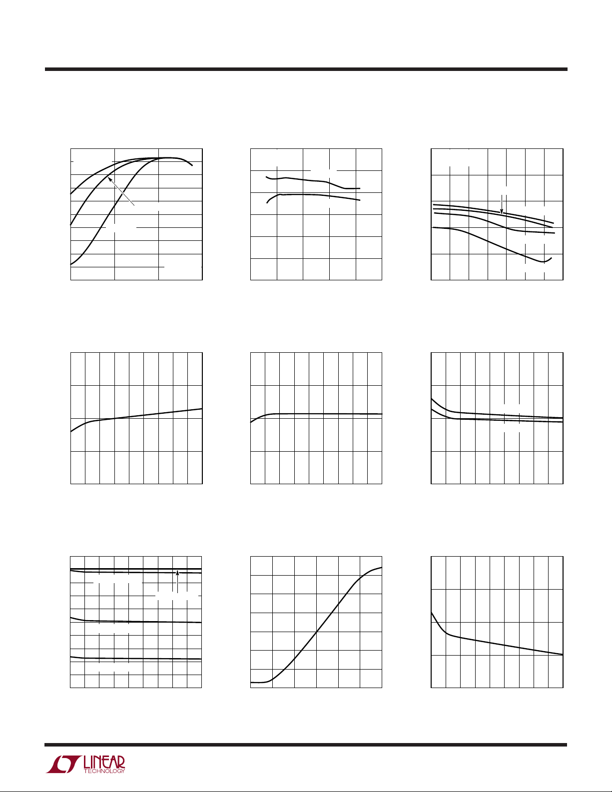
UW
FREQUENCY (kHz)
200
85
EFFICIENCY (%)
100
450
3733 G03
91
88
97
94
250
550350
300
400 500
VIN = 5V
VIN = 12V
VIN = 20V
V
OUT
= 1.5V
I
LOAD
= 20A
VIN = 8V
TEMPERATURE (°C)
–45
65
MAXIMUM I
SENSE
THRESHOLD (mV)
85
45
3733 G06
70
80
75
–30
900
–15
15 7530 60
VO = 1.55V
VO = 0.8V
TEMPERATURE (°C)
–45
3.0
UNDERVOLTAGE RESET (V)
5.0
45
3733 G09
3.5
4.5
4.0
–30
900
–15
15 7530 60
TYPICAL PERFOR A CE CHARACTERISTICS
LTC3733/LTC3733-1
Efficiency vs I
100
V
= OPEN
FCB
90
80
70
60
50
40
EFFICIENCY (%)
30
20
10
0
0.1
V
FCB
INDUCTOR CURRENT (A)
Reference Voltage vs
Temperature
610
605
600
OUT
V
= 5V
FCB
= 0V
VIN = 8V
V
= 1.5V
OUT
1
10
100
3733 G01
Efficiency vs V
100
V
= 1.5V
OUT
f = 210kHz
95
90
85
EFFICIENCY (%)
80
75
70
0
IN
IL = 20A
IL = 50A
5
15
VIN (V)
2510 20
3733 G02
Error Amplifier gm vs
Temperature
4.0
3.5
(mmho)
m
3.0
Efficiency vs Frequency
Maximum I
Threshold vs
SENSE
Temperature
595
REFERENCE VOLTAGE (mV)
590
–45
Oscillator Frequency vs
Temperature
600
550
500
450
400
350
300
FREQUENCY (kHz)
250
200
150
100
–45
–15
–30
TEMPERATURE (°C)
V
= 2.4V
PLLFLTR
V
= 1.2V
PLLFLTR
V
= 0V
PLLFLTR
–30
–15
TEMPERATURE (°C)
15 7530 60
45
V
PLLFLTR
15 7530 60
45
3733 G04
= 5V
3733 G07
2.5
ERROR AMPLIFIER g
900
2.0
–45
–30
–15
15 7530 60
TEMPERATURE (°C)
45
900
3733 G05
Undervoltage Reset Voltage vs
Oscillator Frequency vs V
550
500
450
400
350
FREQUENCY (kHz)
300
250
900
200
0
0.4
1.2 2.0
V
PLLFLTR
(V)
1.6
PLLFLTR
2.40.8
3733 G08
Temperature
3733f
5
LTC3733/LTC3733-1
TEMPERATURE (°C)
–45
0
5
15
SHUTDOWN CURRENT (µA)
40
45
3733 G12
25
35
10
20
30
–30
900
–15
15 7530 60
V
ITH
(V)
0
–20
–10
0
I
SENSE
VOLTAGE THRESHOLD (mV)
10
30
40
50
90
70
1.6
3733 G15
20
80
60
0.8
2.41.2
0.4
2.0
V
OUT
(V)
0
–60
–50
–40
–30
–20
–10
I
SENSE
PIN CURRENT (µA)
0
1.2
3733 G18
0.2
1.60.6
0.4
0.8 1.0 1.4
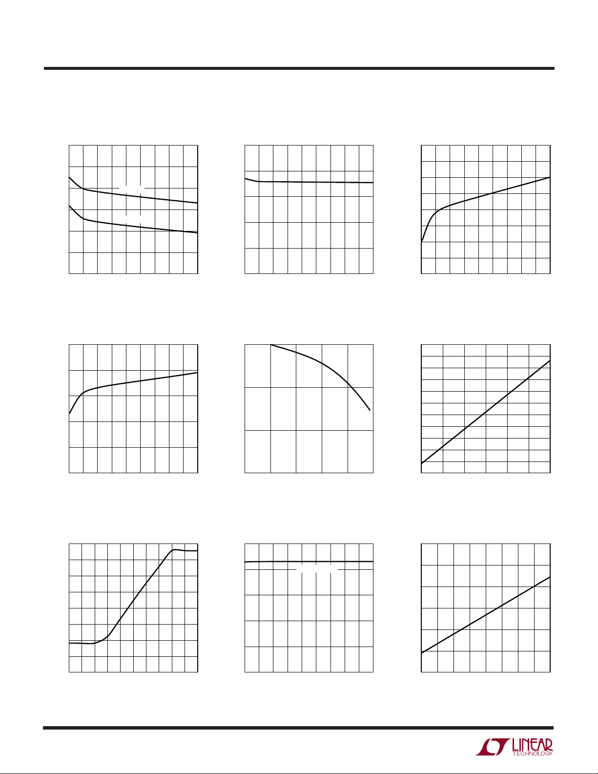
UW
TYPICAL PERFOR A CE CHARACTERISTICS
Short-Circuit Arming and Latchoff
vs Temperature
5.0
4.5
4.0
3.5
3.0
SS PIN VOLTAGE (V)
2.5
2.0
–45
–30
ARMING
LATCHOFF
–15
15 7530 60
TEMPERATURE (°C)
45
SS Pull-Up Current vs
Temperature
2.5
2.0
1.5
3733 G10
Shutdown Current vs
Supply Current vs Temperature
3.0
2.6
2.2
1.8
SUPPLY CURRENT (mA)
1.4
900
1.0
–45
–30
–15
TEMPERATURE (°C)
45
15 7530 60
900
3733 G11
Temperature
Maximum Current Sense
Threshold vs Duty Factor Peak Current Threshold vs V
75
50
ITH
1.0
SS PULL-UP CURRENT (µA)
0.5
0
–45
–30
Percentage of Nominal Output vs
Peak I
80
70
60
50
40
VOLTAGE (mV)
30
SENSE
20
PEAK I
10
0
0
10
PERCENTAGE OF NOMINAL OUTPUT VOLTAGE (%)
6
–15
TEMPERATURE (°C)
(Foldback)
SENSE
40 80
20
30
45
15 7530 60
70
3733 G13
9060
3733 G16
VOLTAGE (mV)
25
SENSE
I
900
0
0
20
DUTY FACTOR (%)
60
10040 80
3733 G14
Maximum Duty Factors vs
Temperature I
100
V
98
96
94
92
MAXIMUM DUTY FACTOR (%)
10050
90
–45
–15
–30
TEMPERATURE (°C)
= 0V
PLLFLTR
45
15 7530 60
900
3733 G17
Pin Current vs V
SENSE
OUT
3733f
UW
TYPICAL PERFOR A CE CHARACTERISTICS
LTC3733/LTC3733-1
Maximum Current Threshold
Mismatch vs Temperature
3.0
2.5
2.0
1.5
1.0
0.5
0
MAXIMUM CURRENT THRESHOLD MISMATCH (mV)
–45
–15
–30
15 7530 60
TEMPERATURE (°C)
45
3733 G19
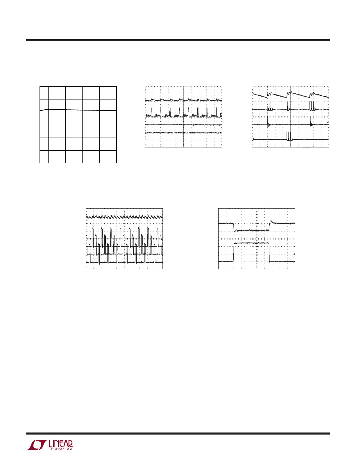
Continuous Mode at 1Amp,
Light Load Current
V
AC, 20mV/DIV
OUT
V
SW1
5V/DIV
AC, 20mV/DIV
900
Shed Mode at 1Amp,
Light Load Current
V
OUT
V
SW1
10V/DIV
V
SW2
10V/DIV
V
SW3
10V/DIV
= 12V
V
IN
= 1.5V
V
OUT
V
= V
FCB
CC
FREQUENCY = 210kHz 3733 G20
4µs/DIV
V
OUT
AC, 50mV/DIV
Burst Mode at 1Amp,
Light Load Current
V
AC, 20mV/DIV
OUT
V
SW1
10V/DIV
V
SW2
10V/DIV
V
SW3
10V/DIV
V
V
V
FREQUENCY = 210kHz
= 12V
IN
OUT
FCB
= 1.5V
= OPEN
Transient Load Current
Response: 0Amp to 50Amp
20µs/DIV
3733 G21
V
SW2
5V/DIV
V
SW3
5V/DIV
V
IN
V
OUT
V
FCB
FREQUENCY = 210kHz
= 12V
= 1.5V
= 0V
4µs/DIV
3733 G22
20A/DIV
I
L
= 12V
V
IN
= 1.5V
V
OUT
V
= 0V
FCB
FREQUENCY = 210kHz
20µs/DIV
3733 G23
3733f
7

LTC3733/LTC3733-1
U
PI FU CTIO S
VID0 to VID4 (Pins 36, 1, 18, 19, 20/Pins 35, 36, 16, 17,
18): Output Voltage Programming Input Pins. A 150k
internal pull-up resistor is provided on each input pin. See
Table 1 for details. Do not apply voltage to these pins prior
to the application of voltage on the VCC pin.
RUN (Pin 2/Pin 37): ON/OFF Control of the LTC3733.
PLLFLTR (Pin 3/Pin 1): The phase-locked loop’s lowpass
filter is tied to this pin. Alternatively, this pin can be driven
with an AC or DC voltage source to vary the frequency of
the internal oscillator. (Do not apply voltage to this pin
prior to the application of voltage on the VCC pin.)
FCB (Pin 4/Pin 2): Forced Continuous Control Input. The
voltage applied to this pin sets the operating mode of the
controller. The forced continuous current mode is active
when the applied voltage is less than 0.6V. Burst Mode
operation will be active when the pin is allowed to float and
a stage shedding mode will be active if the pin is tied to the
VCC pin. (Do not apply voltage to this pin prior to the
application of voltage on the VCC pin.)
IN+, IN– (Pins 5, 6/Pins 3, 4): Inputs to a precision, unitygain differential amplifier with internal precision resistors.
This provides true remote sensing of both the positive and
negative load terminals for precise output voltage control.
DIFFOUT (Pin 7/Pin 5): Output of the Remote Output
Voltage Sensing Differential Amplifier.
EAIN (Pin 8/Pin 6): This is the input to the error amplifier
which compares the VID divided, feedback voltage to the
internal 0.6V reference voltage.
SGND (Pin 9/Pin 7, 39): Signal Ground. This pin must be
routed separately under the IC to the PGND pin and then
to the main ground plane. The exposed pad (QFN) must be
soldered to the PCB for optimal thermal performance.
UU
(G36/QFN)
SENSE1+, SENSE2+, SENSE3+, SENSE1–, SENSE2–,
SENSE3– (Pins 10 to 15/Pins 8 to 13): The Inputs to Each
Differential Current Comparator. The ITH pin voltage and
built-in offsets between SENSE– and SENSE+ pins, in conjunction with R
SS (Pin 16/Pin 14): Combination of Soft-Start and ShortCircuit Detection Timer. A capacitor to ground at this pin
sets the ramp time to full current output as well as the time
delay prior to an output voltage short-circuit shutdown. A
minimum value of 0.01µF is recommended on this pin.
I
(Pin 17/Pin 15): Error Amplifier Output and Switching
TH
Regulator Compensation Point. All three current
comparator’s thresholds increase with this control voltage.
PGND (Pin 26/Pin 24): Driver Power Ground. This pin
connects to the sources of the bottom N-channel external
MOSFETs and the (–) terminals of CIN.
BG1 to BG3 (Pins 27, 25, 24/Pins 25, 23, 22): High
Current Gate Drives for Bottom N-Channel MOSFETs.
Voltage swing at these pins is from ground to VCC.
DRV
External MOSFET Gates in QFN Package. This pin needs to
be closely decoupled to the IC’s PGND pin.
V
the controller circuit power. In the G36 package, it is also
the high power supply to drive the external MOSFET gates
and this pin needs to be closely decoupled to the IC’s
PGND pin.
SW1 to SW3 (Pins 32, 29, 23/Pins 31, 28, 21): Switch
Node Connections to Inductors. Voltage swing at these
pins is from a Schottky diode (external) voltage drop
below ground to VIN (where V
supply rail).
(NA/Pin 26): High Power Supply to Drive the
CC
(Pin 28/Pin 27): Main Supply Pin. This pin supplies
CC
, set the current trip threshold level.
SENSE
is the external MOSFET
IN
8
3733f

LTC3733/LTC3733-1
U
PI FU CTIO S
TG1 to TG3 (Pins 33, 30, 22/Pins 32, 29, 20): High
Current Gate Drives for Top N-channel MOSFETs. These
are the outputs of floating drivers with a voltage swing
equal to the boost voltage source superimposed on the
switch node voltage SW.
BOOST1 to BOOST3 (Pins 34, 31, 21/Pins 33, 30, 19):
Positive Supply Pins to the Topside Floating Drivers.
Bootstrapped capacitors, charged with external Schottky
diodes and a boost voltage source, are connected between
the BOOST and SW pins. Voltage swing at the BOOST pins
is from boost source voltage (typically VCC) to this boost
source voltage + VIN (where V
supply rail).
UU
(G36/QFN)
is the external MOSFET
IN
PGOOD (Pin 35/Pin 34): This open-drain output is pulled
low when the output voltage is outside the PGOOD tolerance window. PGOOD is blanked during VID transitions
for approximately 120µs.
PLLIN (NA/Pin 38): Synchronization Input to Phase Detector. This pin is internally terminated to SGND with
50kΩ. The phase-locked loop will force the rising top gate
signal of controller 1 to be synchronized with the rising
edge of the PLLIN signal. This pin is not available in the
G36 package.
Exposed Pad (NA/Pin 39): Signal Ground. Must be soldered to PCB.
3733f
9
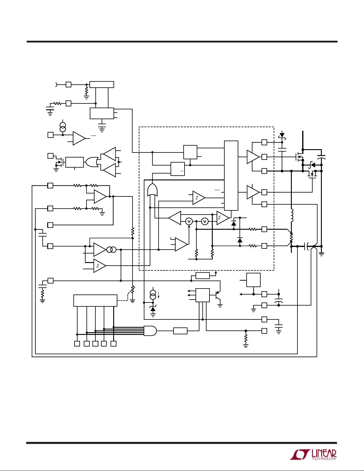
LTC3733/LTC3733-1
U
U
W
FU CTIO AL DIAGRA
PLLIN
(LTC3733-1 ONLY)
F
IN
R
C
FCB
PGOOD
–
IN
+
IN
DIFFOUT
EAIN
I
TH
C
C
R
C
PLLFLTR
LP
LP
2.4V
2.5µA
+
–
0.6V
120µs
BLANKING
VID TRANSITIONS
0.600V
0.660V
PHASE DET
50k
OSCILLATOR
FCB
40k40k
–
A1
+
40k40k
V
FB
–
EA
+
OV
+
–
5-BIT VID DECODER
CLK1
CLK2
CLK3
–
0.66V
+
–
+
0.54V
6.667k
R2 VARIABLE
DUPLICATE FOR SECOND AND THIRD
CONTROLLER CHANNELS
EAIN
R1
LATCH
RS
V
CC
6V
5(VFB)
1.5µA
SLOPE
COMP
SRQ
I
1
5(V
Q
0.55V
–
+
2.4V
SHDN
RST
V
CC
BOOST
DROP
OUT
DET
BOT
FORCE BOT
B
+–
3mV
SHED
RUN
SOFTSTART
FCB
SHDN
45k45k
–
I
+
+
–
+–
)
FB
SWITCH
LOGIC
2
0.600V
INTERNAL
SUPPLY
TOP
V
CC
THE LTC3733-1)
BOT
(DRVCC IN
V
CC
30k
30k
V
REF
TG
SW
BG
PGND
SENSE
SENSE
V
SGND
SS
+
R
SENSE
–
V
CC
CC
+
V
IN
D
B
C
B
L
+
C
IN
C
OUT
+
V
OUT
C
CC
10
VID0 VID1 VID2 VID3 VID4
NO_CPU
1µs
Figure 2
100k
RUN
C
SS
3733 F02
3733f

OPERATIO
LTC3733/LTC3733-1
U
(Refer to Functional Diagram)
Main Control Loop
The IC uses a constant frequency, current mode stepdown architecture. During normal operation, each top
MOSFET is turned on each cycle when the oscillator sets
the RS latch, and turned off when the main current
comparator, I1, resets each RS latch. The peak inductor
current at which I1 resets the RS latch is controlled by the
voltage on the I
amplifier EA. The EAIN pin receives a portion of the voltage
feedback signal via the DIFFOUT pin through the internal
VID DAC and is compared to the internal reference voltage.
When the load current increases, it causes a slight decrease in the EAIN pin voltage relative to the 0.6V reference, which in turn causes the ITH voltage to increase until
each inductor’s average current matches one third of the
new load current (assuming all three current sensing
resistors are equal). In Burst Mode operation and stage
shedding mode, after each top MOSFET has turned off, the
bottom MOSFET is turned on until either the inductor
current starts to reverse, as indicated by current comparator I2, or the beginning of the next cycle.
The top MOSFET drivers are biased from floating bootstrap capacitor CB, which is normally recharged during
each off cycle through an external Schottky diode. When
VIN decreases to a voltage close to V
loop may enter dropout and attempt to turn on the top
MOSFET continuously. The dropout detector counts the
number of oscillator cycles that the bottom MOSFET
remains off and periodically forces a brief on period to
allow CB to recharge.
The main control loop is shut down by pulling the RUN pin
low. Releasing RUN allows an internal 1.5µA current
source to charge soft-start capacitor CSS at the SS pin. The
internal ITH voltage is then clamped to the SS voltage when
CSS is slowly charged up. This “soft-start” clamping
prevents abrupt current from being drawn from the input
power source. When the RUN pin is low, all functions are
kept in a controlled state.
pin, which is the output of the error
TH
, however, the
OUT
forcing temporary forced PWM operation and 2) a logic
input to select between three modes of operation.
When the FCB pin voltage is below 0.6V, the controller
performs as a continuous, PWM current mode synchronous switching regulator. The top and bottom MOSFETs
are alternately turned on to maintain the output voltage
independent of direction of inductor current. When the
FCB pin is below VCC –␣ 1V but greater than 0.6V, the
controller performs as a Burst Mode switching regulator.
Burst Mode operation sets a minimum output current level
before turning off the top switch and turns off the synchronous MOSFET(s) when the inductor current goes negative. This combination of requirements will, at low current,
force the ITH pin below a voltage threshold that will
temporarily shut off both output MOSFETs until the output
voltage drops slightly. There is a burst comparator having
60mV of hysteresis tied to the ITH pin. This hysteresis
results in output signals to the MOSFETs that turn them on
for several cycles, followed by a variable “sleep” interval
depending upon the load current. The resultant output
voltage ripple is held to a very small value by having the
hysteretic comparator after the error amplifier gain block.
When the FCB pin is tied to the VCC pin, Burst Mode
operation is disabled and the forced minimum inductor
current requirement is removed. This provides constant
frequency, discontinuous current operation over the widest possible output current range. At approximately 10%
of maximum designed load current, the second and third
output stages are shut off and the first controller alone is
active in discontinuous current mode. This “stage shedding” optimizes efficiency by eliminating the gate charging
losses and switching losses of the other two output
stages. Additional cycles will be skipped when the output
load current drops below 1% of maximum designed load
current in order to maintain the output voltage. This
constant frequency operation is not as efficient as Burst
Mode operation at very light loads, but does provide lower
noise, constant frequency operating mode down to very
light load conditions.
Low Current Operation
The FCB pin is a multifunction pin: 1) an analog comparator input to provide regulation for a secondary winding by
Tying the FCB pin to ground will force continuous current
operation. This is the least efficient operating mode, but
may be desirable in certain applications. The output can
3733f
11

LTC3733/LTC3733-1
U
OPERATIO
(Refer to Functional Diagram)
source or sink current in this mode. When forcing continuous operation and sinking current, this current will be
forced back into the main power supply, potentially
boosting the input supply to dangerous voltage levels—
BEWARE!
Frequency Synchronization or Setup
The phase-locked loop allows the internal oscillator to be
synchronized to an external source using the PLLIN pin.
The output of the phase detector at the PLLFLTR pin is also
the DC frequency control input of the oscillator which
operates over a 210kHz to 530kHz range corresponding to
a voltage input from 0V to 2.4V. When locked, the PLL
aligns the turn on of the top MOSFET to the rising edge of
the synchronizing signal. When no frequency information
is supplied to the PLLIN pin, PLLFLTR goes low, forcing
the oscillator to minimum frequency. A DC source can be
applied to the PLLFLTR pin to externally set the desired
operating frequency.
In the G36 package, the PLLIN pin is not brought out and
the PLLFLTR pin is for frequency setup only.
Differential Amplifier
Short-Circuit Detection
The SS capacitor is used initially to limit the inrush current
from the input power source. Once the controllers have
been given time, as determined by the capacitor on the SS
pin, to charge up the output capacitors and provide full
load current, the SS capacitor is then used as a shortcircuit timeout circuit. If the output voltage falls to less
than 70% of its nominal output voltage, the SS capacitor
begins discharging, assuming that the output is in a severe
overcurrent and/or short-circuit condition. If the condition
lasts for a long enough period, as determined by the size
of the SS capacitor, the controller will be shut down until
the RUN pin voltage is recycled. This built-in latchoff can
be overridden by providing >5µ A at a compliance of 4V to
the SS pin. This current shortens the soft-start period but
prevents net discharge of the SS capacitor during a severe
overcurrent and/or short-circuit condition. Foldback current limiting is activated when the output voltage falls
below 70% of its nominal level whether or not the shortcircuit latchoff circuit is enabled. Foldback current limit
can be overridden by clamping the EAIN pin such that the
voltage is held above the (70%)(0.6V) or 0.42V level even
when the actual output voltage is low.
This amplifier provides true differential output voltage
sensing. Sensing both V
tion in high current applications and/or applications having electrical interconnection losses. This sensing also
isolates the physical power ground from the physical
signal ground preventing the possibility of troublesome
“ground loops” on the PC layout and prevents voltage
errors caused by board-to-board interconnects, particularly helpful in VRM designs.
Power Good
The PGOOD pin is connected to the drain of an internal
MOSFET. The MOSFET is turned on once the output
voltage has been away from its nominal value by greater
than 10%. The PGOOD signal is blanked for approximately
120µ s during VID transitions. If a new VID transition
occurs before the previous blanking time expires, the
timer is reset.
OUT
+
and V
–
benefits regula-
OUT
The SS capacitor will be reset if the input voltage, (VCC) is
allowed to fall below approximately 4V. The capacitor on
the pin will be discharged until the short-circuit arming
latch is disarmed. The SS capacitor will attempt to cycle
through a normal soft-start ramp up after the VCC supply
rises above 4V. This circuit prevents power supply latchoff
in the event of input power switching break-before-make
situations.
No_CPU Detection
The LTC3733 detects the presense of CPU by monitoring
all VID bits. If an all-“1” condition is detected, the controller acknowledges a No_CPU fault. If this fault condition
persists for more than 1µ s, the SS pin is pulled low and the
controller is shut down.
3733f
12

WUUU
APPLICATIO S I FOR ATIO
LTC3733/LTC3733-1
The basic application circuit is shown in Figure 1 on the
first page of this data sheet. External component selection
is driven by the load requirement, and normally begins
with the selection of an inductance value based upon the
desired operating frequency, inductor current and output
voltage ripple requirements. Once the inductors and
operating frequency have been chosen, the current sensing resistors can be calculated. Next, the power MOSFETs
and Schottky diodes are selected. Finally, CIN and C
OUT
are selected according to the required voltage ripple
requirements. The circuit shown in Figure 1 can be
configured for operation up to a MOSFET supply voltage
of 28V (limited by the external MOSFETs).
Operating Frequency
The IC uses a constant frequency architecture with the
frequency determined by an internal capacitor. This capacitor is charged by a fixed current plus an additional
current which is proportional to the voltage applied to the
PLLFLTR pin. Refer to the Phase-Locked Loop and Frequency Synchronization and Setup sections for additional
information.
Inductor Value Calculation and Output Ripple Current
The operating frequency and inductor selection are interrelated in that higher operating frequencies allow the use
of smaller inductor and capacitor values. So why would
anyone ever choose to operate at lower frequencies with
larger components? The answer is efficiency. A higher
frequency generally results in lower efficiency because of
MOSFET gate charge and transition losses. In addition to
this basic tradeoff, the effect of inductor value on ripple
current and low current operation must also be considered. The PolyPhase approach reduces both input and
output ripple currents while optimizing individual output
stages to run at a lower fundamental frequency, enhancing
efficiency.
The inductor value has a direct effect on ripple current. The
inductor ripple current ∆IL per individual section, N,
decreases with higher inductance or frequency and increases with higher VIN or V
V
∆I
OUT OUT
=−
L
fL
V
1
V
IN
:
OUT
A graph for the voltage applied to the PLLFLTR pin versus
frequency is given in Figure 3. As the operating frequency
is increased the gate charge losses will be higher, reducing
efficiency (see Efficiency Considerations). The maximum
switching frequency is approximately 530kHz.
550
450
350
250
OPERATING FREQUENCY (kHz)
150
0 0.5 1.0 1.5 2.0 2.5
Figure 3. Operating Frequency vs V
PLLFLTR PIN VOLTAGE (V)
3733 F03
PLLFLTR
where f is the individual output stage operating frequency.
In a PolyPhase converter, the net ripple current seen by the
output capacitor is much smaller than the individual
inductor ripple currents due to the ripple cancellation. The
details on how to calculate the net output ripple current
can be found in Application Note 77.
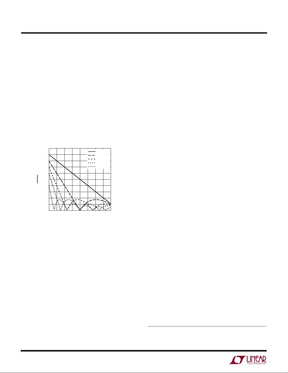
Figure 4 shows the net ripple current seen by the output
capacitors for the different phase configurations. The
output ripple current is plotted for a fixed output voltage as
the duty factor is varied between 10% and 90% on the
x-axis. The output ripple current is normalized against the
inductor ripple current at zero duty factor. The graph can
be used in place of tedious calculations. As shown in
Figure 4, the zero output ripple current is obtained when:
V
OUT
V
k
==12 1, ,..., –
where k N
N
IN
3733f
13
LTC3733/LTC3733-1
WUUU
APPLICATIO S I FOR ATIO
So the number of phases used can be selected to minimize
the output ripple current and therefore the output ripple
voltage at the given input and output voltages. In applications having a highly varying input voltage, additional
phases will produce the best results.
Accepting larger values of ∆IL allows the use of low
inductances but can result in higher output voltage ripple.
A reasonable starting point for setting ripple current is
∆IL = 0.4(I
I
is the total load current. Remember, the maximum
OUT
)/N, where N is the number of channels and
OUT
∆IL occurs at the maximum input voltage. The individual
inductor ripple currents are constant determined by the
inductor, input and output voltages.
1.0
0.9
0.8
0.7
0.6
/fL
0.5
O
O(P-P)
V
I
0.4
0.3
0.2
0.1
0
0.1 0.2 0.3 0.4
Figure 4. Normalized Peak Output Current
vs Duty Factor [I
DUTY FACTOR (V
0.5 0.6 0.7 0.8 0.9
= 0.3(I
RMS
OUT/VIN
1-PHASE
2-PHASE
3-PHASE
4-PHASE
6-PHASE
)
O(P-P)
3733 F04
]
Inductor Core Selection
Once the value for L1 to L3 is known, the type of inductor
must be selected. High efficiency converters generally
cannot afford the core loss found in low cost powdered
iron cores, forcing the use of ferrite, molypermalloy or
Kool Mµ® cores. Actual core loss is independent of core
size for a fixed inductor value, but it is very dependent on
inductance selected. As inductance increases, core losses
go down. Unfortunately, increased inductance requires
more turns of wire and therefore copper losses will
increase.
Ferrite designs have very low core loss and are preferred
at high switching frequencies, so design goals can
concentrate on copper loss and preventing saturation.
Ferrite core material saturates “hard,” which means that
inductance collapses abruptly when the peak design
current is exceeded. This results in an abrupt increase in
inductor ripple current and consequent output voltage
ripple. Do not allow the core to saturate!
Power MOSFET and D1, D2, D3 Selection
At least two external power MOSFETs must be selected for
each of the three output sections: One N-channel MOSFET
for the top (main) switch and one or more N-channel
MOSFET(s) for the bottom (synchronous) switch. The
number, type and “on” resistance of all MOSFETs selected
take into account the voltage step-down ratio as well as the
actual position (main or synchronous) in which the MOSFET
will be used. A much smaller and much lower input
capacitance MOSFET should be used for the top MOSFET
in applications that have an output voltage that is less than
1/3 of the input voltage. In applications where VIN >> V
OUT
,
the top MOSFETs’ “on” resistance is normally less important for overall efficiency than its input capacitance at
operating frequencies above 300kHz. MOSFET manufacturers have designed special purpose devices that provide
reasonably low “on” resistance with significantly reduced
input capacitance for the main switch application in switching regulators.
The peak-to-peak MOSFET gate drive levels are set by the
voltage, VCC, requiring the use of logic-level threshold
MOSFETs in most applications. Pay close attention to the
BV
specification for the MOSFETs as well; many of the
DSS
logic-level MOSFETs are limited to 30V or less.
Selection criteria for the power MOSFETs include the “on”
resistance R
, input capacitance, input voltage and
SD(ON)
maximum output current.
MOSFET input capacitance is a combination of several
components but can be taken from the typical “gate
charge” curve included on most data sheets (Figure 5).
The curve is generated by forcing a constant input current
Kool Mµ is a registered trademark of Magnetics, Inc.
14
3733f

WUUU
APPLICATIO S I FOR ATIO
V
IN
V
GS
into the gate of a common source, current source loaded
stage and then plotting the gate voltage versus time. The
initial slope is the effect of the gate-to-source and the gateto-drain capacitance. The flat portion of the curve is the
result of the Miller capacitance effect of the drain-tosource capacitance as the drain drops the voltage across
the current source load. The upper sloping line is due to
the drain-to-gate accumulation capacitance and the gateto-source capacitance. The Miller charge (the increase in
coulombs on the horizontal axis from a to b while the curve
is flat) is specified for a given VDS drain voltage, but can be
adjusted for different VDS voltages by multiplying by the
ratio of the application VDS to the curve specified V
values. A way to estimate the C
change in gate charge from points a and b on a manufacturers data sheet and divide by the stated VDS voltage
specified. C
for determining the transition loss term in the top MOSFET
but is not directly specified on MOSFET data sheets. C
and COS are specified sometimes but definitions of these
parameters are not included.
When the controller is operating in continuous mode the
duty cycles for the top and bottom MOSFETs are given by:
Main SwitchDuty Cycle
Synchronous Switch Duty Cycle
MILLER EFFECT
ab
=
MILLER
V
OUT
V
IN
V
Q
C
MILLER
IN
= (QB – QA)/V
Figure 5. Gate Charge Characteristic
MILLER
DS
is the most important selection criteria
V
GS
V
DS
3733 F05
term is to take the
VV
–
IN OUT
=
V
IN
DS
RSS
LTC3733/LTC3733-1
The power dissipation for the main and synchronous
MOSFETs at maximum output current are given by:
V
P
MAIN
OUTINMAX
=
V
V
IN
I
2
MAX
2
–
VV V
CC TH MIN TH MIN
VV
–
P
SYNC
IN OUTINMAX
=
V
where N is the number of output stages, δ is the temperature dependency of R
resistance (approximately 2Ω at VGS = V
drain potential
and
particular application. V
typical gate threshold voltage specified in the power
MOSFET data sheet. C
using the gate charge curve from the MOSFET data sheet
and the technique described above.
Both MOSFETs have I2R losses while the topside N-channel
equation includes an additional term for transition losses,
which peak at the highest input voltage. For VIN < 12V, the
high current efficiency generally improves with larger
MOSFETs, while for V
rapidly increase to the point that the use of a higher
R
device with lower C
DS(ON)
efficiency. The synchronous MOSFET losses are greatest
at high input voltage when the top switch duty factor is low
or during a short circuit when the synchronous switch is
on close to 100% of the period.
The term (1 + δ ) is generally given for a MOSFET in the
form of a normalized R
2
I
N
RC
()( )
DR MILLER
N
11
() ()
I
N
DS(ON)
R
+
1
δ
()
DS ON
+
()
•
+
2
+
1
()
f
()
R
δ
DS ON
()
, RDR is the effective top driver
), VIN is the
MILLER
the change in drain potential in the
TH(MIN)
MILLER
DS(ON)
is the data sheet specified
is the calculated capacitance
> 12V, the transition losses
IN
actually provides higher
RSS
vs temperature curve, but
3733f
15
LTC3733/LTC3733-1
WUUU
APPLICATIO S I FOR ATIO
δ = 0.005/°C can be used as an approximation for low
voltage MOSFETs.
The Schottky diodes, D1 to D3 shown in Figure 1 conduct
during the dead time between the conduction of the two
large power MOSFETs. This prevents the body diode of the
bottom MOSFET from turning on, storing charge during
the dead time and requiring a reverse recovery period
which could cost as much as several percent in efficiency.
A 2A to 8A Schottky is generally a good compromise for
both regions of operation due to the relatively small
average current. Larger diodes result in additional transition losses due to their larger junction capacitance.
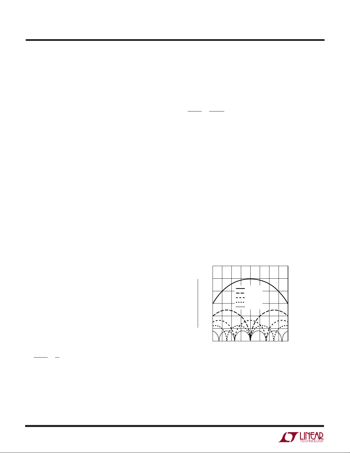
CIN and C
Selection
OUT
Input capacitance ESR requirements and efficiency losses
are reduced substantially in a multiphase architecture
because the peak current drawn from the input capacitor
is effectively divided by the number of phases used and
power loss is proportional to the RMS current squared. A
3-stage, single output voltage implementation can reduce
input path power loss by 90%.
In continuous mode, the source current of each top
N-channel MOSFET is a square wave of duty cycle V
OUT/VIN
.
A low ESR input capacitor sized for the maximum RMS
current must be used. The details of a close form equation
can be found in Application Note 77. Figure 6 shows the
input capacitor ripple current for different phase configurations with the output voltage fixed and input voltage
varied. The input ripple current is normalized against the
DC output current. The graph can be used in place of
tedious calculations. The minimum input ripple current
can be achieved when the product of phase number and
output voltage, N(V
), is approximately equal to the
OUT
input voltage VIN or:
V
OUT
V
k
==12 1, ,..., –
where k N
N
IN
So the phase number can be chosen to minimize the input
capacitor size for the given input and output voltages.
In the graph of Figure 6, the local maximum input RMS
capacitor currents are reached when:
V
OUT
V
21
k
==
IN
where k N
N
12–, ,...,
These worst-case conditions are commonly used for design because even significant deviations do not offer much
relief. Note that capacitor manufacturer’s ripple current
ratings are often based on only 2000 hours of life. This
makes it advisable to further derate the capacitor or to
choose a capacitor rated at a higher temperature than required. Several capacitors may also be paralleled to meet
size or height requirements in the design. Always consult
the capacitor manufacturer if there is any question.
The Figure 6 graph shows that the peak RMS input current
is reduced linearly, inversely proportional to the number N
of stages used. It is important to note that the efficiency
loss is proportional to the input RMS current squared and
therefore a 3-stage implementation results in 90% less
power loss when compared to a single phase design.
Battery/input protection fuse resistance (if used), PC
0.6
0.5
0.4
0.3
0.2
DC LOAD CURRENT
RMS INPUT RIPPLE CURRNET
0.1
0
0.1 0.2 0.3 0.4 0.5 0.6 0.7 0.8
Figure 6. Normalized Input RMS Ripple Current
vs Duty Factor for One to Six Output Stages
DUTY FACTOR (V
1-PHASE
2-PHASE
3-PHASE
4-PHASE
6-PHASE
OUT/VIN
0.9
)
3733 F06
16
3733f

WUUU
APPLICATIO S I FOR ATIO
LTC3733/LTC3733-1
board trace and connector resistance losses are also
reduced by the reduction of the input ripple current in a
PolyPhase system. The required amount of input capacitance is further reduced by the factor, N, due to the
effective increase in the frequency of the current pulses.
Ceramic capacitors are becoming very popular for small
designs but several cautions should be observed. “X7R”,
“X5R” and “Y5V” are examples of a few of the ceramic
materials used as the dielectric layer, and these different
dielectrics have very different effect on the capacitance
value due to the voltage and temperature conditions
applied. Physically, if the capacitance value changes due
to applied voltage change, there is a concommitant piezo
effect which results in radiating sound! A load that draws
varying current at an audible rate may cause an attendant
varying input voltage on a ceramic capacitor, resulting in
an audible signal. A secondary issue relates to the energy
flowing back into a ceramic capacitor whose capacitance
value is being reduced by the increasing charge. The
voltage can increase at a considerably higher rate than the
constant current being supplied because the capacitance
value is decreasing as the voltage is increasing! Ceramic
capacitors, when properly selected and used however, can
provide the lowest overall loss due to their extremely low
ESR.
The selection of C
series resistance (ESR). Typically once the ESR requirement is satisfied the capacitance is adequate for filtering.
The steady-state output ripple (∆V
∆∆V I ESR
where f = operating frequency of each stage, N is the
number of output stages, C
∆IL = ripple current in each inductor. The output ripple is
highest at maximum input voltage since ∆IL increases
≈+
OUT RIPPLE
is driven by the required effective
OUT
) is determined by:
OUT
NfC
8
= output capacitance and
OUT
1
OUT
with input voltage. The output ripple will be less than 50mV
at max VIN with ∆IL = 0.4I
C
required ESR < N • R
OUT
and
C
> 1/(8Nf)(R
OUT
The emergence of very low ESR capacitors in small,
surface mount packages makes very small physical implementations possible. The ability to externally compensate
the switching regulator loop using the ITH pin allows a
much wider selection of output capacitor types. The
impedance characteristics of each capacitor type is significantly different than an ideal capacitor and therefore
requires accurate modeling or bench evaluation during
design.
Manufacturers such as Nichicon, United Chemicon and
Sanyo should be considered for high performance throughhole capacitors. The OS-CON semiconductor dielectric
capacitor available from Sanyo and the Panasonic SP
surface mount types have a good (ESR)(size) product.
Once the ESR requirement for C
RMS current rating generally far exceeds the I
requirement. Ceramic capacitors from AVX, Taiyo Yuden,
Murata and Tokin offer high capacitance value and very
low ESR, especially applicable for low output voltage
applications.
In surface mount applications, multiple capacitors may
have to be paralleled to meet the ESR or RMS current
handling requirements of the application. Aluminum electrolytic and dry tantalum capacitors are both available in
surface mount configurations. New special polymer surface mount capacitors offer very low ESR also but have
much lower capacitive density per unit volume. In the case
of tantalum, it is critical that the capacitors are surge tested
for use in switching power supplies. Several excellent
choices are the AVX TPS, AVX TPSV, the KEMET T510
SENSE
OUT(MAX)
)
SENSE
assuming:
has been met, the
OUT
RIPPLE(P-P)
3733f
17

LTC3733/LTC3733-1
WUUU
APPLICATIO S I FOR ATIO
series of sur
series of surface mount special polymer capacitors available in case heights ranging from 2mm to 4mm. Other
capacitor types include Sanyo POS-CAP, Sanyo OS-CON,
Nichicon PL series and Sprague 595D series. Consult the
manufacturer for other specific recommendations.
R
SENSE
Once the frequency and inductor have been chosen,
R
SENSE1, RSENSE2, RSENSE3
required peak inductor current. The current comparator
has a maximum threshold of 75mV/R
common mode range of SGND to (1.1) • VCC. The current
comparator threshold sets the peak inductor current,
yielding a maximum average output current I
the peak value less half the peak-to-peak ripple current,
∆IL.
Allowing a margin for variations in the IC and external
component values yields:
RN
SENSE
The IC works well with values of R
0.02Ω.
VCC Decoupling
The VCC pin supples power not only the internal circuits of
the controller but also the top and bottom gate drivers and
therefore must be bypassed very carefully to ground with
a ceramic capacitor, type X7R or X5R (depending upon
the operating temperature environment) of
imme
diately next to the IC
10µF placed very close to the IC due to the extremely high
instantaneous currents involved. The total capacitance,
taking into account the voltage coefficient of ceramic
capacitors, should be 100 times as large as the total
combined gate charge capacitance of ALL of the MOSFETs
being driven. Good bypassing close to the IC is necessary
face-mount tantalums or the Panasonic SP
Selection for Output Current
are determined based on the
and an input
SENSE
MAX
mV
50
=
I
MAX
from 0.001Ω to
SENSE
at least 1µF
and preferably an additional
equal to
to supply the high transient currents required by the
MOSFET gate drivers while keeping the 5V supply quiet
enough so as not to disturb the very small-signal high
bandwidth of the current comparators.
Topside MOSFET Driver Supply (CB, DB)
External bootstrap capacitors, CB, connected to the BOOST
pins, supply the gate drive voltages for the topside
MOSFETs. Capacitor CB in the Functional Diagram is
charged though diode DB from VCC when the SW pin is
low. When one of the topside MOSFETs turns on, the
driver places the CB voltage across the gate-source of the
desired MOSFET. This enhances the MOSFET and turns on
the topside switch. The switch node voltage, SW, rises to
VIN and the BOOST pin follows. With the topside MOSFET
on, the boost voltage is above the input supply (V
VCC + VIN). The value of the boost capacitor CB needs to be
30 to 100 times that of the total input capacitance of the
topside MOSFET(s). The reverse breakdown of DB must be
greater than V
Differential Amplifier
The IC has a true remote voltage sense capability. The
sensing connections should be returned from the load,
back to the differential amplifier’s inputs through a common, tightly coupled pair of PC traces. The differential
amplifier rejects common mode signals capacitively or
inductively radiated into the feedback PC traces as well as
ground loop disturbances. The differential amplifier output signal is divided down through the VID DAC and is
compared with the internal, precision 0.6V voltage reference by the error amplifier.
The amplifier has a 0 to VCC common mode input range
and an output swing range of 0 to V
uses an NPN emitter follower with 80kΩ feedback resistance. A DC resistive load to ground is required in order to
sink more current.
IN(MAX).
– 1.2V. The output
CC
BOOST
=
18
3733f

WUUU
APPLICATIO S I FOR ATIO
LTC3733/LTC3733-1
Output Voltage
The IC includes a digitally controlled 5-bit attenuator
producing output voltages as defined in Table 1. Output
voltages with 25mV increments are produced from 0.8V to
1.55V.
Each VID digital input is pulled up to a logical high with an
internal 150k resistor. The input logic threshold is approximately 1.2V but the input circuit can withstand an
input voltage of up to 7V.
ON/OFF Control
The RUN pin provides simple ON/OFF control for the
LTC3733. Driving the RUN pin above 1.5V permits the
controller to start operating. Pulling RUN below 0.8V puts
the LTC3733 into low current shutdown (IQ ≈ 20µA).
Soft-Start Function
The SS pin provides two functions: 1) soft-start and 2) a
defeatable short-circuit latch off timer. Soft-start reduces
the input power sources’ surge currents by gradually
increasing the controller’s current limit (proportional to an
internal buffered and clamped V
). The latchoff timer
ITH
prevents very short, extreme load transients from tripping
the overcurrent latch. A small pull-up current (>5µA)
supplied to the SS pin will prevent the overcurrent latch
from operating. The following explanation describes how
this function operates.
An internal 1.5µA current source charges up the C
SS
capacitor. As the voltage on SS increases from 0V to 2.4V,
the internal current limit is increased from 0V/R
75mV/R
. The output current limit ramps up slowly,
SENSE
SENSE
to
taking 1.6s/µF to reach full current. The output current
thus ramps up slowly, eliminating the starting surge
current required from the input power supply.
Table 1. VID Output Voltage Programming
VID4 VID3 VID2 VID1 VID0 V
0 0 0 0 0 1.550
0 0 0 0 1 1.525
0 0 0 1 0 1.500
0 0 0 1 1 1.475
0 0 1 0 0 1.450
0 0 1 0 1 1.425
0 0 1 1 0 1.400
0 0 1 1 1 1.375
0 1 0 0 0 1.350
0 1 0 0 1 1.325
0 1 0 1 0 1.300
0 1 0 1 1 1.275
0 1 1 0 0 1.250
0 1 1 0 1 1.225
0 1 1 1 0 1.200
0 1 1 1 1 1.175
1 0 0 0 0 1.150
1 0 0 0 1 1.125
1 0 0 1 0 1.100
1 0 0 1 1 1.075
1 0 1 0 0 1.050
1 0 1 0 1 1.025
1 0 1 1 0 1.000
1 0 1 1 1 0.975
1 1 0 0 0 0.950
1 1 0 0 1 0.925
1 1 0 1 0 0.900
1 1 0 1 1 0.875
1 1 1 0 0 0.850
1 1 1 0 1 0.825
1 1 1 1 0 0.800
1 1 1 1 1 Shutdown
OUT
VV
24 0
t
IRAMP SS SS
=
.–
A
µ
15
.
CsFC
=µ
16
./
()
The SS pin has an internal 6V zener clamp (see the
Functional Diagram).
3733f
19

LTC3733/LTC3733-1
WUUU
APPLICATIO S I FOR ATIO
Fault Conditions: Overcurrent Latchoff
The SS pin also provides the ability to latch off the
controllers when an overcurrent condition is detected. The
SS capacitor is used initially to limit the inrush current of
all three output stages. After the controllers have been
given adequate time to charge up the output capacitor and
provide full load current, the SS capacitor is used for a
short-circuit timer. If the output voltage falls to less than
70% of its nominal value, the SS capacitor begins discharging on the assumption that the output is in an
overcurrent condition. If the condition lasts for a long
enough period, as determined by the size of the SS
capacitor, the controller will be shut down until the RUN
pin voltage is recycled. If the overload occurs during startup, the time can be approximated by:
t
>> (CSS • 0.6V)/(1.5µA) = 4 • 105 (CSS)
LO1
If the overload occurs after start-up, the voltage on the SS
capacitor will continue charging and will provide additional time before latching off:
t
>> (CSS • 3V)/(1.5µA) = 2 • 106 (CSS)
LO2
This built-in overcurrent latchoff can be overridden by
providing a pull-up resistor to the SS pin from VCC as
shown in Figure 7. When VCC is 5V, a 200k resistance will
prevent the discharge of the SS capacitor during an
overcurrent condition but also shortens the soft-start
period, so a larger SS capacitor value will be required.
Why should you defeat overcurrent latchoff? During the
prototyping stage of a design, there may be a problem with
noise pick-up or poor layout causing the protection circuit
to latch off the controller. Defeating this feature allows
troubleshooting of the circuit and PC layout. The internal
foldback current limiting still remains active, thereby
protecting the power supply system from failure. A decision can be made after the design is complete whether to
rely solely on foldback current limiting or to enable the
latchoff feature by removing the pull-up resistor.
The value of the soft-start capacitor CSS may need to be
scaled with output current, output capacitance and load
current characteristics. The minimum soft-start capacitance is given by:
CSS > (C
OUT
)(V
) (10–4) (R
OUT
SENSE
)
The minimum recommended soft-start capacitor of
CSS = 0.1µF will be sufficient for most applications.
Current Foldback
In certain applications, it may be desirable to defeat the
internal current foldback function. A negative impedance
is experienced when powering a switching regulator.
That
is, the input current is higher at a lower VIN and
decreases as VIN is increased. Current foldback is designed to accommodate a normal, resistive load having
increasing current draw with increasing voltage. The EAIN
pin should be artificially held 70% above its nominal
operating level of 0.6V, or 0.42V in order to prevent the IC
from “folding back” the peak current level. A suggested
circuit is shown in Figure 8.
V
CC
V
CC
20
V
Figure 7. Defeating Overcurrent Latchoff
SS PIN
CC
R
SS
C
SS
3733 F07
Q1
CALCULATE FOR
0.42V TO 0.55V
Figure 8. Foldback Current Elimination
LTC3733
EAIN
3733 F08
3733f

WUUU
APPLICATIO S I FOR ATIO
LTC3733/LTC3733-1
The emitter of Q1 will hold up the EAIN pin to a voltage in
the absence of V
that will prevent the internal sensing
OUT
circuitry from reducing the peak output current. Removing the function in this manner eliminates the external
MOSFET’s protective feature under short-circuit conditions. This technique will also prevent the short-circuit
latchoff function from turning off the part during a shortcircuit event and the output current will only be limited to
N • 75mV/R
SENSE
.
Undervoltage Reset
In the event that the input power source to the IC (VCC)
drops below 4V, the SS capacitor will be discharged to
ground and the controller will be shut down. When V
CC
rises above 4V, the SS capacitor will be allowed to recharge and initiate another soft-start turn-on attempt. This
may be useful in applications that switch between two
supplies that are not diode connected, but note that this
cannot make up for the resultant interruption of the
regulated output.
Phase-Locked Loop and
Frequency Synchronization (LTC3733-1)
The IC has a phase-locked loop comprised of an internal
voltage controlled oscillator and phase detector. This
allows the top MOSFET of output stage 1’s turn-on to be
locked to the rising edge of an external source. The
frequency range of the voltage controlled oscillator is
±50% around the center frequency fO. A voltage applied to
the PLLFLTR pin of 1.2V corresponds to a frequency of
approximately 350kHz. The nominal operating frequency
range of the IC is 210kHz to 530kHz.
The phase detector used is an edge sensitive digital type
that provides zero degrees phase shift between the
external and internal oscillators. This type of phase
detector will not lock the internal oscillator to harmonics
of the input frequency. The PLL hold-in range, ∆fH, is
equal to the capture range, ∆fC:
The output of the phase detector is a complementary pair
of current sources charging or discharging the external
filter components on the PLLFLTR pin. A simplified block
diagram is shown in Figure 9.
If the external frequency (f
lator frequency, f
, current is sourced continuously,
OSC
) is greater than the oscil-
PLLIN
pulling up the PLLFLTR pin. When the external frequency
is less than f
, current is sunk continuously, pulling
OSC
down the PLLFLTR pin. If the external and internal frequencies are the same, but exhibit a phase difference, the
current sources turn on for an amount of time corresponding to the phase difference. Thus, the voltage on the
PLLFLTR pin is adjusted until the phase and frequency of
the external and internal oscillators are identical. At this
stable operating point, the phase comparator output is
open and the filter capacitor CLP holds the voltage. The IC
PLLIN pin must be driven from a low impedance source
such as a logic gate located close to the pin. When using
multiple ICs for a phase-locked system, the PLLFLTR pin
of the master oscillator should be biased at a voltage that
will guarantee the slave oscillator(s) ability to lock onto the
master’s frequency. A voltage of 1.7V or below applied to
the master oscillator’s PLLFLTR pin is recommended in
order to meet this requirement. The resultant operating
frequency will be approximately 500kHz for 1.7V.
R
LP
3733 F09
10k
PLLFLTR
OSC
C
LP
PHASE
DETECTOR/
OSC
OSCILLATOR
FREQUENCY
50k
DIGITAL
PHASE/
DETECTOR
EXTERNAL
PLLIN
(LTC3733-1
ONLY)
Figure 9. Phase-Locked Loop Block Diagram
2.4V
∆fH = ∆fC = ±0.5 f
O
3733f
21

LTC3733/LTC3733-1
WUUU
APPLICATIO S I FOR ATIO
The loop filter components (CLP, RLP) smooth out the
current pulses from the phase detector and provide a
stable input to the voltage controlled oscillator. The filter
components CLP and RLP determine how fast the loop
acquires lock. Typically R
0.01µF to 0.1µF.
Minimum On-Time Considerations
Minimum on-time, t
that the IC is capable of turning on the top MOSFET. It is
determined by internal timing delays and the gate charge
of the top MOSFET. Low duty cycle applications may
approach this minimum on-time limit and care should be
taken to ensure that:
t
ON MIN
If the duty cycle falls below what can be accommodated by
the minimum on-time, the IC will begin to skip every other
cycle, resulting in half-frequency operation. The output
voltage will continue to be regulated, but the ripple current
and ripple voltage will increase.
The minimum on-time for the IC is generally about 120ns.
However, as the peak sense voltage decreases the minimum on-time gradually increases. This is of particular
concern in forced continuous applications with low ripple
current at light loads. If the duty cycle drops below the
minimum on-time limit in this situation, a significant
amount of cycle skipping can occur with correspondingly
larger current and voltage ripple.
If an application can operate close to the minimum ontime limit, an inductor must be chosen that is low enough
in value to provide sufficient ripple amplitude to meet the
minimum on-time requirement.
<
()
ON(MIN)
V
OUT
Vf
()
IN
=10k and CLP ranges from
LP
, is the smallest time duration
As a general rule, keep
the inductor ripple current equal to or greater than 30%
of I
OUT(MAX)
at V
IN(MAX)
.
Efficiency Considerations
The percent efficiency of a switching regulator is equal to
the output power divided by the input power times 100%.
It is often useful to analyze individual losses to determine
what is limiting the efficiency and which change would
produce the most improvement. Percent efficiency can be
expressed as:
%Efficiency = 100% – (L1 + L2 + L3 + ...)
where L1, L2, etc. are the individual losses as a percentage
of input power.
Checking Transient Response
The regulator loop response can be checked by looking at
the load transient response. Switching regulators take
several cycles to respond to a step in DC (resistive) load
current. When a load step occurs, V
amount equal to ∆I
series resistance of C
discharge C
forces the regulator to adapt to the current change and
return V
time, V
ringing, which would indicate a stability problem. The
availability of the ITH pin not only allows optimization of
control loop behavior, but also provides a DC coupled
and AC filtered closed-loop response test point. The DC
step, rise time and settling at this test point truly reflects
the closed-loop response. Assuming a predominantly
second order system, phase margin and/or damping
factor can be estimated using the percentage of overshoot
seen at this pin. The bandwidth can also be estimated by
examining the rise time at the pin. The ITH external components shown in the Figure 1 circuit will provide an
adequate starting point for most applications.
OUT
OUT
, generating the feedback error signal that
OUT
to its steady-state value. During this recovery
can be monitored for excessive overshoot or
• ESR, where ESR is the effective
LOAD
OUT
. ∆I
also begins to charge or
LOAD
shifts by an
OUT
22
3733f

µ
WUUU
APPLICATIO S I FOR ATIO
LTC3733/LTC3733-1
The I
loop compensation. The values can be modified slightly
(from 0.2 to 5 times their suggested values) to maximize
transient response once the final PC layout is done and the
particular output capacitor type and value have been
determined. The output capacitors need to be decided
upon because the various types and values determine the
loop feedback factor gain and phase. An output current
pulse of 20% to 80% of full load current having a rise time
of <2µ s will produce output voltage and ITH pin waveforms
that will give a sense of the overall loop stability without
breaking the feedback loop. The initial output voltage step,
resulting from the step change in output current, may not
be within the bandwidth of the feedback loop, so this signal
cannot be used to determine phase margin. This is why it
is better to look at the ITH pin signal which is in the
feedback loop and is the filtered and compensated control
loop response. The gain of the loop will be increased by
increasing RC and the bandwidth of the loop will be
increased by decreasing CC. If RC is increased by the same
factor that CC is decreased, the zero frequency will be kept
the same, thereby keeping the phase the same in the most
critical frequency range of the feedback loop. The output
voltage settling behavior is related to the stability of the
closed-loop system and will demonstrate the actual overall supply performance.
A second, more severe transient is caused by switching in
loads with large (>1µF) supply bypass capacitors. The
discharged bypass capacitors are effectively put in parallel
with C
alter its delivery of current quickly enough to prevent this
sudden step change in output voltage if the load switch
resistance is low and it is driven quickly. If C
than 2% of C
so that the load rise time is limited to approximately
1000 • R
series RC-CC filter sets the dominant pole-zero
TH
, causing a rapid drop in V
OUT
, the switch rise time should be controlled
OUT
SENSE
• C
. Thus a 250µ F capacitor and a 2mΩ
LOAD
. No regulator can
OUT
is greater
LOAD
R
the charging current to about 1A.
Design Example (Using Three Phases)
As a design example, assume V
20V(max), V
inductance value is chosen first based upon a 30% ripple
current assumption. The highest value of ripple current in
each output stage occurs at the maximum input voltage.
Using L = 0.6µH, a commonly available value results in
34% ripple current. The worst-case output ripple for the
three stages operating in parallel will be less than 11% of
the peak output current.
R
a conservative maximum sense current threshold of 65mV
and taking into account half of the ripple current:
Use a commonly available 0.003Ω sense resistor.
Next verify the minimum on-time is not violated. The
minimum on-time occurs at maximum VCC:
resistor would require a 500µs rise time, limiting
SENSE
= 12V(nominal), V
IN
= 1.3V, I
OUT
V
OUT OUT
L
=
fIVV
()
=
400 30 15
()()()
068
.
≥
SENSE1, RSENSE2
R
SENSE
t
ON MIN
()
−
1
∆
kHz A
13
.
IN
V
%
H
and R
mV
=
65
34
A
15 1
=
+
V
OUT
Vf
IN MAX
()
()
= 45A and f = 400kHz. The
MAX
V
13
.
1
−
SENSE3
can be calculated by using
=Ω
0 0037
%
2
=
.
V kHz
20 400
()
V
20
V
.13
=
162
ns
IN
=
3733f
23

LTC3733/LTC3733-1
WUUU
APPLICATIO S I FOR ATIO
The output voltage will be set by the VID code according
to Table 1.
The power dissipation on the topside MOSFET can be
estimated. Using a Fairchild FDS6688 for example, R
= 7mΩ, C
voltage with T(estimated) = 50°C:
The worst-case power dissipation by the synchronous
MOSFET under normal operating conditions at elevated
ambient temperature and estimated 50°C junction temperature rise is:
P
A short circuit to ground will result in a folded back current
of:
P
MAIN
SYNC
MILLER
≈
=
= 15nC/15V = 1000pF. At maximum input
V
.
18
V
20
.
0 007 20
VV V
518
VV
20 1 3
20
2
15 1 0 005 50 25
()+()
+
Ω
()
1
–. .
−
.
V
.
[]
45
2
23
()()
1
+
15 1 25 0 007 1 84
()()
()
18
2
AW
CC
°− °
()
A
2 1000
Ω
()( )
=
kHz W
400 2 2
.. .
()
pF
.
Ω
=
DS(ON)
IC. These items are also illustrated graphically in the layout
diagram of Figure 10. Check the following in the PC layout:
1) Are the signal and power ground paths isolated? Keep the
SGND at one end of a printed circuit path thus preventing
MOSFET currents from traveling under the IC. The IC signal
ground pin should be used to hook up all control circuitry
on one side of the IC, routing the copper through SGND,
under the IC covering the “shadow” of the package, connecting to the PGND pin and then continuing on to the (–) plates
of C
and C
IN
placed immediately adjacent to the IC between the VCC pin
and PGND. A 1µ F ceramic capacitor of the X7R or X5R type
is small enough to fit very close to the IC to minimize the ill
effects of the large current pulses drawn to drive the bottom
MOSFETs. An additional 5µ F to 10uF of ceramic, tantalum
or other very low ESR capacitance is recommended in order to keep the internal IC supply quiet. The power ground
returns to the sources of the bottom N-channel MOSFETs,
anodes of the Schottky diodes and (–) plates of CIN, which
should have as short lead lengths as possible.
2) Does the IC IN+ pin connect to the (+) plates of C
A 30pF to 300pF feedforward capacitor between the
DIFFOUT and EAIN pins should be placed as close as
possible to the IC.
. The VCC decoupling capacitor should be
OUT
OUT
?
ns V
mV
I
SC
with a typical value of R
0.25. The resulting power dissipated in the bottom MOSFET
is:
P
SYNC
which is less than one third of the normal, full load
conditions. Incidentally, since the load no longer dissipates any power, total system power is decreased by over
90%. Therefore, the system actually cools significantly
during a shorted condition!
PC Board Layout Checklist
When laying out the printed circuit board, the following
checklist should be used to ensure proper operation of the
25
≈
= (7.5A)2(1.25)(0.007Ω) ≈ 0.5W
m
+
23
()
Ω
1
+
2
DS(ON)
150 20
0675.
and d = (0.005/°C)(50°C) =
()
H
µ
=
.
A
3) Are the SENSE– and SENSE+ printed circuit traces for
each channel routed together with minimum PC trace
spacing? The filter capacitors between SENSE+ and SENSE
for each channel should be as close as possible to the pins
of the IC. Connect the SENSE– and SENSE+ pins to the pads
of the sense resistor as illustrated in Figure 11.
4) Do the (+) plates of CIN connect to the drains of the
topside MOSFETs as closely as possible? This capacitor
provides the pulsed current to the MOSFETs.
5) Keep the switching nodes, SWITCH, BOOST and TG
away from sensitive small-signal nodes. Ideally the
SWITCH, BOOST and TG printed circuit traces should be
routed away and separated from the IC and the “quiet” side
of the IC.
6) The filter capacitors between the ITH and SGND pins
should be as close as possible to the pins of the IC.
–
3733f
24

WUUU
APPLICATIO S I FOR ATIO
SW1
LTC3733/LTC3733-1
L1
R
SENSE1
D1
V
IN
R
IN
+
C
IN
BOLD LINES INDICATE HIGH,
SWITCHING CURRENT LINES.
KEEP LINES TO A MININMUM
LENGTH
L2
SW2
D2
SW3
D3
R
SENSE2
L3
R
SENSE3
Figure 10. Branch Current Waveforms
C
OUT
3732 F10
V
OUT
+
R
L
INDUCTOR
LTC3733
+
SENSE
SENSE
1000pF
–
OUTPUT CAPACITOR
SENSE
RESISTOR
3733 F11
Figure 11. Kelvin Sensing R
SENSE
3733f
25

LTC3733/LTC3733-1
WUUU
APPLICATIO S I FOR ATIO
Figure 10 illustrates all branch currents in a three-phase
switching regulator. It becomes very clear after studying
the current waveforms why it is critical to keep the high
switching current paths to a small physical size. High electric and magnetic fields will radiate from these “loops” just
as radio stations transmit signals. The output capacitor
ground should return to the negative terminal of the input
capacitor and not share a common ground path with any
switched current paths. The left half of the circuit gives rise
to the “noise” generated by a switching regulator. The
ground terminations of the synchronous MOSFETs and
Schottky diodes should return to the bottom plate(s) of the
input capacitor(s) with a short isolated PC trace since very
high switched currents are present. A separate isolated path
from the bottom plate(s) of the input and output capacitor(s)
should be used to tie in the IC power ground pin (PGND).
This technique keeps inherent signals generated by high
current pulses taking alternate current paths that have
SINGLE PHASE
SW V
finite impedances during the total period of the switching
regulator. External OPTI-LOOP compensation allows overcompensation for PC layouts which are not optimized but
this is not the recommended design procedure.
Simplified Visual Explanation of How a 3-Phase
Controller Reduces Both Input and Output RMS
Ripple Current
The effect of multiphase power supply design significantly
reduces the amount of ripple current in both the input and
output capacitors. The RMS input ripple current is divided
by, and the effective ripple frequency is multiplied up by
the number of phases used (assuming that the input
voltage is greater than the number of phases used times
the output voltage). The output ripple amplitude is also
reduced by, and the effective ripple frequency is increased
by the number of phases used. Figure 12 graphically
illustrates the principle.
I
CIN
I
COUT
TRIPLE PHASE
SW1 V
SW2 V
SW3 V
I
L1
I
L2
I
L3
I
CIN
I
COUT
Figure 12. Single and Polyphase Current Waveforms
3732 F12
26
3733f

WUUU
APPLICATIO S I FOR ATIO
LTC3733/LTC3733-1
The worst-case input RMS ripple current for a single stage
design peaks at twice the value of the output voltage. The
worst-case input RMS ripple current for a two stage
design results in peaks at 1/4 and 3/4 of the input voltage,
and the worst-case input RMS ripple current for a three
stage design results in peaks at 1/6, 1/2, and 5/6 of the
input voltage. The peaks, however, are at ever decreasing
levels with the addition of more phases. A higher effective
duty factor results because the duty factors “add” as long
as the currents in each stage are balanced. Refer to AN19
for a detailed description of how to calculate RMS current
for the single stage switching regulator.
Figure 6 illustrates the RMS input current drawn from the
input capacitance versus the duty cycle as determined by
the ration of input and output voltage. The peak input RMS
current level of the single phase system is reduced by 2/3
in a 3-phase solution due to the current splitting between
the three stages.
The output ripple current is reduced significantly when
compared to the single phase solution using the same
inductance value because the V
/L discharge currents
OUT
term from the stages that has their bottom MOSFETs on
subtract current from the (VCC – V
)/L charging current
OUT
resulting from the stage which has its top MOSFET on. The
output ripple current for a 3-phase design is:
V
=
fL
()()
OUT
DC V V
13 3–
()
>
IN OUT
I
P-P
The ripple frequency is also increased by three, further
reducing the required output capacitance when VCC < 3V
OUT
as illustrated in Figure 4.
Efficiency Calculation
To estimate efficiency, the DC loss terms include the input
and output capacitor ESR, each MOSFET R
tor resistance RL, the sense resistance R
DS(ON)
SENSE
, induc-
and the
forward drop of the Schottky rectifier at the operating
output current and temperature. Typical values for the
design example given previously in this data sheet are:
Main MOSFET R
Sync MOSFET R
C
C
= 20mΩ
INESR
OUTESR
= 3mΩ
= 7mΩ (9mΩ at 90°C)
DS(ON)
= 7mΩ (9mΩ at 90°C)
DS(ON)
RL = 2.5mΩ
R
V
V
= 3mΩ
SENSE
SCHOTTKY
= 1.3V
OUT
= 0.8V at 15A (0.7V at 90°C)
VIN = 12V
I
= 0.8V at 15A (0.7V at 90°C)
MAX
δ = 0.01%°C
N = 3
f = 400kHz
The main MOSFET is on for the duty factor V
OUT/VIN
and
the synchronous MOSFET is on for the rest of the period
or simply (1 – V
OUT/VIN
). Assuming the ripple current is
small, the AC loss in the inductor can be made small if a
good quality inductor is chosen. The average current,
I
is used to simplify the calaculations. The equation
OUT
below is not exact but should provide a good technique
for the comparison of selected components and give a
result that is within 10% to 20% of the final application.
3733f
27

LTC3733/LTC3733-1
WUUU
APPLICATIO S I FOR ATIO
The temperature of the MOSFET’s die temperature may
require interative calculations if one is not familiar typical
performance. A maximum operating junction temperature of 90° to 100°C for the MOSFETs is recommended
for high reliability applications.
Common output path DC loss:
2
I
PN
COMPATH
This totals 3.375W + C
≈
MAX
R R C Loss
()
L SENSE OUTESR
N
OUTESR
+
loss.
+
Total of all three main MOSFET’s DC loss:
PN
MAIN
=
V
OUTINMAX
V
This totals 0.83W + C
I
N
INESR
2
R C Loss
1δ
+
()
DS ON INESR
()
loss.
+
Total of all three synchronous MOSFET’s DC loss:
PN
SYNC
=
V
11
–
OUTINMAX
V
2
I
()
N
+
δ
R
DS ON
()
Total of all three synchronous MOSFET’s AC loss:
V
() () ()( ) ( )361545Q
IN
fnC
G
V
DSSPEC
=
This totals 0.08W at V
= 8V, 0.12W at VIN = 12V and
IN
V
IN
V
DSSPEC
E
0.19W at VIN = 20V. The bottom MOSFET does not
experience the Miller capacitance dissipation issue that
the main switch does because the bottom switch turns on
when its drain is close to ground.
The Schottky rectifier loss assuming 50ns nonoverlap
time:
2 • 3(0.7V)(15A)(50ns)(4E5)
This totals 1.26W.
The total output power is (1.3V)(45A) = 58.5W and the
total input power is approximately 60W so the % loss of
each component is as follows:
Main switch AC loss (VIN = 12V) 2.25W 3.75%
Main switch DC loss 0.83W 1.4%
Synchronous switch AC loss 0.19W 0.3%
This totals 5.4W.
Total of all three main MOSFET’s AC loss:
A
45
PV
≈Ω
MAIN IN
2
3
()
()()
1
VV V
518
–. .
2 1000
()( )
23
1
+
18
pF
kHz W
400 6 3
().
=
This totals 1W at VIN = 8V, 2.25W at VIN = 12V and 6.25W
at VIN = 20V.
Synchronous switch DC loss 5.4W 9%
Power path loss 3.375W 5.6%
The numbers above represent the values at VIN = 12V. It
can be seen from this simple example that two things can
be done to improve efficiency: 1) Use two MOSFETs on the
synchronous side and 2) use a smaller MOSFET for the
main switch with smaller C
to better balance the AC
MILLER
loss with the DC loss. A smaller, less expensive MOSFET
can actually perform better in the task of the main switch.
28
3733f
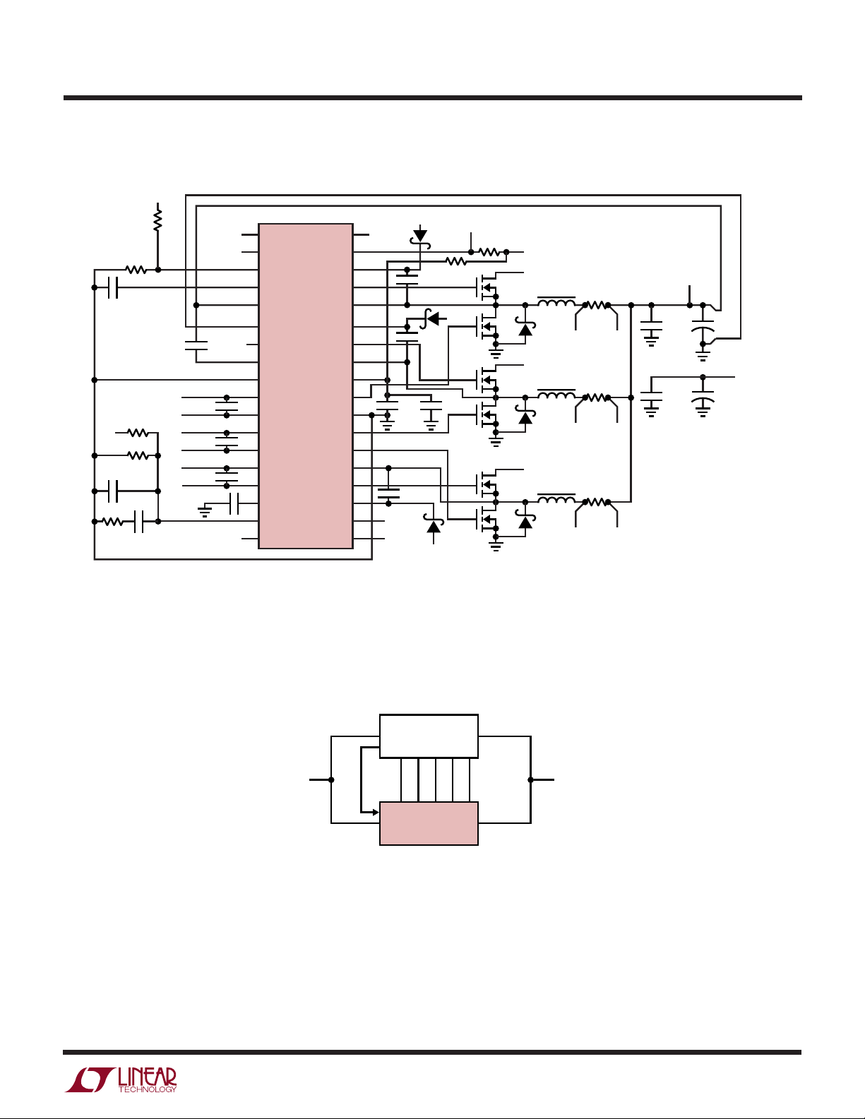
TYPICAL APPLICATIO
V
CC
51k
VID1 IN
10k
100pF
+
S1
1000pF
–
S1
71.5k
5V
22.1k
100pF
220pF
1k
VIN: 7V TO 21V
: 0.8V TO 1.55V, 65A
V
OUT
SWITCHING FREQUENCY: 300kHz
+
S2
1000pF
–
S2
–
S3
1000pF
+
S3
0.1µF
ON/OFF
30pF
VID2 IN
1
2
3
4
5
6
7
8
9
10
11
12
13
14
15
16
17
18
CIN: SANYO OS-CON 25SP68M
C
OUT
D1 TO D3: MBRS340T3
U
65A Power Supply for AMD Opteron Processors
V
CC
0.1µF
0.1µF
V
PGOOD
47k
1Ω
V
CC
10µF
CC
36
VID0 IN
35
34
33
32
31
30
29
28
V
CC
27
26
25
24
23
22
21
20
19
1µF
0.1µF
VID4 IN
VID3 IN
3733 TA01
LTC3733
+
–
+
–
–
+
VID0
PGOOD
BOOST1
TG1
SW1
BOOST2
TG2
SW2
BG1
PGND
BG2
BG3
SW3
TG3
BOOST3
VID4
VID3
VID1
RUN
PLLFLTR
FCB
+
IN
–
IN
DIFFOUT
EAIN
SGND
SENSE1
SENSE1
SENSE2
SENSE2
SENSE3
SENSE3
SS
I
TH
VID2
: 330µF/2.5V ×10 SANYO POSCAP 2R5TPE330M9
LTC3733/LTC3733-1
V
CC
5V
V
IN
M1
M2 D1
M3
M4 D2
M5
M6 D3
L1 TO L3: 0.68µH SUMIDA CEP125-0R6
M1, M3, M5: HAT2168H ×1 OR IRF7811W ×2 OR Si7860DP ×1
M2, M4, M6: HAT2165H ×2 OR IRF7822 ×2 OR Si7892DP ×2
L1
0.002Ω
+
0.002Ω
+
0.002Ω
+
–
S1
–
S2
–
S3
S1
V
IN
L2
S2
V
IN
L3
S3
10µF
6.3V
×3
10µF
35V
×5
V
OUT
+
C
OUT
V
C
IN
68µF
25V
7V TO 21V
+
IN
Block Diagram—6-Phase LTC3731/LTC3733-1 Supply
3-PHASE LTC3731
CLKOUT
V
V
IN
CLK
60°
PLLIN
+
TH
I
EAIN
3-PHASE LTC3733-1
IN–IN
DIFFOUT
3733 TA02
OUT
0.8V TO 1.55V
90A TO 120A
3733f
29

LTC3733/LTC3733-1
PACKAGE DESCRIPTIO
U
G Package
36-Lead Plastic SSOP (5.3mm)
(Reference LTC DWG # 05-08-1640)
1.25 ±0.12
12.50 – 13.10*
(.492 – .516)
2526 22 21 20 19232427282930313233343536
7.8 – 8.2
0.42 ±0.03 0.65 BSC
RECOMMENDED SOLDER PAD LAYOUT
5.00 – 5.60**
(.197 – .221)
0.09 – 0.25
(.0035 – .010)
NOTE:
1. CONTROLLING DIMENSION: MILLIMETERS
2. DIMENSIONS ARE IN
3. DRAWING NOT TO SCALE
*
DIMENSIONS DO NOT INCLUDE MOLD FLASH. MOLD FLASH
SHALL NOT EXCEED .152mm (.006") PER SIDE
**
DIMENSIONS DO NOT INCLUDE INTERLEAD FLASH. INTERLEAD
FLASH SHALL NOT EXCEED .254mm (.010") PER SIDE
0.55 – 0.95
(.022 – .037)
MILLIMETERS
(INCHES)
° – 8°
0
5.3 – 5.7
12345678 9 10 11 12 14 15 16 17 1813
0.65
(.0256)
BSC
0.22 – 0.38
(.009 – .015)
7.40 – 8.20
(.291 – .323)
2.0
(.079)
0.05
(.002)
G36 SSOP 0802
30
3733f

PACKAGE DESCRIPTIO
5.50 ± 0.05
(2 SIDES)
4.10 ± 0.05
(2 SIDES)
3.20 ± 0.05
(2 SIDES)
U
UHF Package
38-Lead Plastic QFN (7mm × 5mm)
(Reference LTC DWG # 05-08-1701)
0.25 ± 0.05
0.50 BSC
5.20 ± 0.05 (2 SIDES)
6.10 ± 0.05 (2 SIDES)
7.50 ± 0.05 (2 SIDES)
RECOMMENDED SOLDER PAD LAYOUT
LTC3733/LTC3733-1
0.70 ± 0.05
PACKAGE
OUTLINE
7.00 ± 0.10
(2 SIDES)
0.75 ± 0.05
5.00 ± 0.10
(2 SIDES)
PIN 1
TOP MARK
(SEE NOTE 6)
NOTE:
1. DRAWING CONFORMS TO JEDEC PACKAGE
OUTLINE M0-220 VARIATION WHKD
2. DRAWING NOT TO SCALE
3. ALL DIMENSIONS ARE IN MILLIMETERS
0.75 ± 0.05
0.00 – 0.05
5.15 ± 0.10
(2 SIDES)
0.200 REF
0.200 REF
0.00 – 0.05
4. DIMENSIONS OF EXPOSED PAD ON BOTTOM OF PACKAGE DO NOT INCLUDE
MOLD FLASH. MOLD FLASH, IF PRESENT, SHALL NOT EXCEED 0.20mm ON ANY SIDE
5. EXPOSED PAD SHALL BE SOLDER PLATED
6. SHADED AREA IS ONLY A REFERENCE FOR PIN 1 LOCATION
ON THE TOP AND BOTTOM OF PACKAGE
0.25 ± 0.05
0.50 BSC
3.15 ± 0.10
(2 SIDES)
BOTTOM VIEW—EXPOSED PAD
37
38
R = 0.115
TYP
0.435
0.18
1
0.23
2
0.40 ± 0.10
(UH) QFN 0303
0.18
Information furnished by Linear Technology Corporation is believed to be accurate and reliable.
However, no responsibility is assumed for its use. Linear Technology Corporation makes no representation that the interconnection of its circuits as described herein will not infringe on existing patent rights.
3733f
31

LTC3733/LTC3733-1
RELATED PARTS
PART NUMBER DESCRIPTION COMMENTS
LTC1628 2-Phase, Dual Output Synchronous Step-Down Reduces CIN and C
DC/DC Controllers 3.5V ≤ VIN ≤ 36V, I
LTC1629/ 20A to 200A PolyPhase Synchronous Controllers Expandable from 2-Phase to 12-Phase, Uses All
LTC1629-PG Surface Mount Components, No Heat Sink, V
LTC1702 No R
TM
2-Phase Dual Synchronous Step-Down 550kHz, No Sense Resistor
SENSE
Controller
LTC1703 No R
Controller with 5-Bit Mobile VID Control V
2-Phase Dual Synchronous Step-Down Mobile Pentium® III Processors, 550kHz,
SENSE
IN
≤ 7V
LTC1708-PG 2-Phase, Dual Synchronous Controller with Mobile VID 3.5V ≤ VIN ≤ 36V, VID Sets V
LT®1709/ High Efficiency, 2-Phase Synchronous Step-Down 1.3V ≤ V
≤ 3.5V, Current Mode Ensures
OUT
LT1709-8 Switching Regulators with 5-Bit VID Accurate Current Sharing, 3.5V ≤ V
LTC1735 High Efficiency Synchronous Step-Down Output Fault Protection, 16-Pin SSOP
Switching Regulator
LTC1736 High Efficiency Synchronous Controller with 5-Bit Mobile Output Fault Protection, 24-Pin SSOP,
VID Control 3.5V ≤ V
LTC1778 No R
Controller I
Current Mode Synchronous Step-Down Up to 97% Efficiency, 4V ≤ VIN ≤ 36V, 0.8V ≤ V
SENSE
OUT
≤ 36V
IN
up to 20A
LTC1929/ 2-Phase Synchronous Controllers Up to 42A, Uses All Surface Mount Components,
LTC1929-PG No Heat Sinks, 3.5V ≤ VIN ≤ 36V
LTC3708 Dual, 2-Phase, No R
Synchronous Buck with Up/Down Output Voltage Tracking, Track Up to 8 Supplies,
SENSE
Output Tracking Fast Transient Response
LTC3711 No R
Controller with Digital 5-Bit Interface 0.925V ≤ V
Current Mode Synchronous Step-Down Up to 97% Efficiency, Ideal for Pentium III Processors,
SENSE
OUT
LTC3719 2-Phase, 5-Bit VID Current Mode, High Efficiency AMD Hammer-K8 Processors, Wide VIN Range: 4V to 36V Operation
Synchronous Step-Down Controller
LTC3729 20A to 200A, 550kHz PolyPhase Synchronous Controller Expandable from 2-Phase to 12-Phase, Uses all Surface Mount
Components, V
LTC3731 3-Phase, 600kHz Synchronous Buck Expandable from 3-Phase to 12-Phase, Uses all Surface Mount
Switching Regulator Controller Components, V
LTC3732 3-Phase, 5-Bit VID, 600kHz Synchronous Buck VRM9.0 and VRM9.1 (VID = 1.1V to 1.85V)
Switching Regulator Controller
No R
is a trademark of Linear Technology Corporation. Pentium is a registered trademark of Intel Corporation.
SENSE
, Power Good Output Signal, Synchronizable,
OUT
up to 20A, 0.8V ≤ V
OUT
, PGOOD
OUT1
IN
≤ 2V, 4V ≤ VIN ≤ 36V, I
up to 36V
IN
up to 36V
IN
≤ 36V
OUT
up to 20A
OUT
≤ 5V
up to 36V
IN
≤ (0.9)(VIN),
OUT
32
Linear Technology Corporation
1630 McCarthy Blvd., Milpitas, CA 95035-7417
(408) 432-1900 ● FAX: (408) 434-0507
●
www.linear.com
3733f
LT/TP 1203 1K • PRINTED IN USA
LINEAR TE CHNO LOGY CORP O R ATIO N 2003
 Loading...