


CHANGE NOTIFICATION
Linear Technology Corporation
(408) 432-1900
August 15, 2008
Dear Sir/Madam:
Subject:
Please be advised that Linear Technology Corporation has made a minor change to the LTC3728
datasheet to more accurately reflect the device performance and optimize limits. The changes are
shown on the attached page of the marked up datasheet. There was no change made to the die. The
product shipped after September 15, 2008 will be tested to the new limits.
Should you have any further questions, please feel free to contact me at (408)-432-1900 ext. 2519, or
by e-mail at NGIRN@linear.com. If I do not hear from you by September 15, 2008, we will consider
this change to be approved by your company.
Sincerely,
Naib Girn
Quality Assurance Manager
Notification of Change to LTC3728 Datasheet
1630 McCarthy Blvd., Milpitas, CA 95035-7417
PCN#: 081508
Confidential Statement
This change notice is for Linear Technology’s Customers only.
Distribution or notification to third parties is prohibited
FEATURES
LTC3728
Dual, 550kHz, 2-Phase
Synchronous Step-Down Switching Regulator
U
DESCRIPTIO
■
Dual, 180° Phased Controllers Reduce Required
Input Capacitance and Power Supply Induced Noise
■
OPTI-LOOP® Compensation Minimizes C
■
±1% Output Voltage Accuracy
■
Power Good Output Voltage Indicator
■
Phase-Lockable Fixed Frequency 250kHz to 550kHz
■
Dual N-Channel MOSFET Synchronous Drive
■
Wide VIN Range: 3.5V to 36V Operation
■
Very Low Dropout Operation: 99% Duty Cycle
■
Adjustable Soft-Start Current Ramping
■
Foldback Output Current Limiting
■
Latched Short-Circuit Shutdown with Defeat Option
■
Output Overvoltage Protection
■
Remote Output Voltage Sense
■
Low Shutdown IQ: 20µA
■
5V and 3.3V Regulators
■
3 Selectable Operating Modes: Constant Frequency,
Burst Mode
■
Available in 32-Pin 5mm × 5mm QFN and
®
Operation and PWM
OUT
28-Pin SSOP Packages
U
APPLICATIO S
■
Notebook and Palmtop Computers
■
Telecom Systems
■
Portable Instruments
■
Battery-Operated Digital Devices
■
DC Power Distribution Systems
The LTC
®
3728 is a dual high performance step-down
switching regulator controller that drives all N-channel
synchronous power MOSFET stages. A constant frequency current mode architecture allows phase-lockable
frequency of up to 550kHz. Power loss and noise due to
the ESR of the input capacitors are minimized by operating
the two controller output stages out of phase.
OPTI-LOOP compensation allows the transient response
to be optimized over a wide range of output capacitance and
ESR values. The precision 0.8V reference and power good
output indicator are compatible with future microprocessor generations, and a wide 3.5V to 30V (36V maximum)
input supply range encompasses all battery chemistries.
A RUN/SS pin for each controller provides both soft-start
and optional timed, short-circuit shutdown. Current
foldback limits MOSFET dissipation during short-circuit
conditions when overcurrent latchoff is disabled. Output
overvoltage protection circuitry latches on the bottom
MOSFET until V
returns to normal. The FCB mode pin
OUT
can select among Burst Mode, constant frequency mode
and continuous inductor current mode or regulate a
secondary winding. The LTC3728 includes a power good
output pin that indicates when both outputs are within
7.5% of their designed set point.
, LT, LTC and LTM are registered trademarks of Linear Technology Corporation.
Burst Mode and OPTI-LOOP are registered trademarks of Linear Technology Corporation.
All other trademarks are the property of their respective owners.
Protected by U.S. Patents, including 5481178, 5929620, 6177787, 6144194, 6100678,
5408150, 6580258, 6304066, 5705919.
TYPICAL APPLICATIO
3.2µH
R
SENSE1
0.01Ω
V
OUT1
5V
5A
C
+
47µF
6V
SP
M1, M2: FDS6982S
U
+
OUT1
4.7µF
M1
L1
R2
105k
1%
R1
20k
1%
1000pF
C
220pF
R
C1
15k
C1
C
B1
500kHz
, 0.1µF
f
IN
D3
C
0.1µF
SS1
VINPGOOD INTV
TG1 TG2
BOOST1 BOOST2
SW1 SW2
LTC3728
BG1 BG2
PLLIN
+
SENSE1
–
SENSE1
V
OSENSE1
I
TH1
RUN/SS1 RUN/SS2
SGND
PGND
SENSE2
SENSE2
V
OSENSE2
CC
I
TH2
+
–
C
0.1µF
C
B2
SS2
Figure 1. High Efficiency Dual 5V/3.3V Step-Down Converter
D4
, 0.1µF
1000pF
220pF
1µF
C
C2
R
C2
15k
V
IN
5.2V TO 28V
C
IN
22µF
50V
M2
L2
3.2µH
R
SENSE2
0.01Ω
V
+
3728 F01
3.3V
5A
OUT2
3728fc
R4
63.4k
C
1%
R3
20k
1%
56µF
OUT
6V
SP
1
LTC3728
323331 30 29 28 27 26 25
9 10 11 12 13
TOP VIEW
14 15 16
17
18
19
20
21
22
23
24
8
7
6
5
4
3
2
1V
OSENSE1
PLLFLTR
PLLIN
FCB
I
TH1
SGND
3.3V
OUT
I
TH2
BOOST1
V
IN
BG1
EXTV
CC
INTV
CC
PGND
BG2
BOOST2
NC
SENSE1–SENSE1+NC
RUN/SS1
PGOOD
TG1
SW1
V
OSENSE2
NC
SENSE2
–
SENSE2
+
RUN/SS2
TG2
SW2
NC
WWWU
ABSOLUTE AXI U RATI GS
(Note 1)
Input Supply Voltage (VIN).........................36V to –0.3V
Top Side Driver Voltages
(BOOST1, BOOST2) ...................................42V to –0.3V
Switch Voltage (SW1, SW2) .........................36V to – 5V
INTV
EXTVCC, RUN/SS1, RUN/SS2, (BOOST1-SW1),
CC,
(BOOST2-SW2), PGOOD ............................. 7V to – 0.3V
SENSE1
SENSE2
+
, SENSE2+, SENSE1–,
–
Voltages ........................ (1.1)INTVCC to –0.3V
PLLIN, PLLFLTR, FCB, Voltage ............ INTVCC to –0.3V
I
TH1, ITH2
, V
OSENSE1
, V
OSENSE2
Peak Output Current <10µs (TG1, TG2, BG1, BG2) ... 3A
INTV
Peak Output Current ................................ 50mA
CC
Operating Temperature Range (Note 7) ... –40°C to 85°C
Junction Temperature (Note 2)............................. 125°C
Storage Temperature Range ................. –65°C to 125°C
Lead Temperature (Soldering, 10 sec)
(G Package Only) .................................................. 300°C
UU
W
PACKAGE/ORDER I FOR ATIO
TOP VIEW
RUN/SS1
SENSE1
SENSE1
V
OSENSE1
PLLFLTR
PLLIN
FCB
I
SGND
3.3V
OUT
I
V
OSENSE2
SENSE2
SENSE2
1
+
2
–
3
4
5
6
7
8
TH1
9
10
11
TH2
12
–
13
+
14
G PACKAGE
28-LEAD PLASTIC SSOP
T
= 125°C, θJA = 95°C/W
JMAX
28
27
26
25
24
23
22
21
20
19
18
17
16
15
PGOOD
TG1
SW1
BOOST1
V
IN
BG1
EXTV
CC
INTV
CC
PGND
BG2
BOOST2
SW2
TG2
RUN/SS2
Order Options Tape and Reel: Add #TR
Lead Free: Add #PBF Lead Free Tape and Reel: Add #TRPBF Lead Free Part Marking: http://www.linear.com/leadfree/
ORDER PART
NUMBER
LTC3728EG
32-LEAD (5mm × 5mm) PLASTIC QFN
EXPOSED PAD IS SGND (MUST BE SOLDERED TO PCB)
UH PACKAGE
T
= 125°C, θJA = 34°C/W
JMAX
Voltages ...2.7V to –0.3V
ORDER PART
NUMBER
LTC3728EUH
UH PART
MARKING
3728
Consult LTC Marketing for parts specified with wider operating temperature ranges.
ELECTRICAL CHARACTERISTICS
temperature range, otherwise specifications are at TA = 25°C. VIN = 15V, V
SYMBOL PARAMETER CONDITIONS MIN TYP MAX UNITS
Main Control Loops
V
I
V
V
2
OSENSE1, 2
VOSENSE1, 2
REFLNREG
LOADREG
Regulated Feedback Voltage (Note 3); I
Feedback Current (Note 3) –5 – 50 nA
Reference Voltage Line Regulation VIN = 3.6V to 30V (Note 3) 0.002 0.02 %/V
Output Voltage Load Regulation (Note 3)
Measured in Servo Loop; ∆I
Measured in Servo Loop; ∆I
The ● denotes the specifications which apply over the full operating
= 5V unless otherwise noted.
●
0.792 0.800 0.808 V
●
●
0.1 0.5 %
–0.1 –0.5 %
Voltage = 1.2V
TH1, 2
RUN/SS1, 2
Voltage = 1.2V to 0.7V
TH
Voltage = 1.2V to 2.0V
TH
3728fc
LTC3728
ELECTRICAL CHARACTERISTICS
temperature range, otherwise specifications are at T
The ● denotes the specifications which apply over the full operating
= 25°C. VIN = 15V, V
A
RUN/SS1, 2
= 5V unless otherwise noted.
SYMBOL PARAMETER CONDITIONS MIN TYP MAX UNITS
g
m1, 2
g
mGBW1, 2
Transconductance Amplifier g
m
Transconductance Amplifier GBW I
I
= 1.2V; Sink/Source 5uA; (Note 3) 1.3 mmho
TH1, 2
= 1.2V; (Note 3) 3 MHzI
TH1, 2
Input DC Supply Current (Note 4)
V
FCB
I
FCB
V
BINHIBIT
Normal Mode V
Shutdown V
= 15V; EXTVCC Tied to V
IN
RUN/SS1, 2
= 0V 20 35 µA
Forced Continuous Threshold
Forced Continuous Pin Current V
= 0.85V – 0.50 – 0.18 –0.1 µA
FCB
Burst Inhibit (Constant Frequency) Measured at FCB pin 4.3 4.8 V
OUT1
; V
= 5V 450 µA
OUT1
●
0.76 0.800 0.84 V
Threshold
UVLO Undervoltage Lockout VIN Ramping Down
V
OVL
I
SENSE
DF
MAX
I
RUN/SS1, 2
V
RUN/SS1, 2
V
RUN/SS1, 2
I
SCL1, 2
I
SDLHO
V
SENSE(MAX)
Feedback Overvoltage Lockout Measured at V
Sense Pins Total Source Current (Each Channel); V
OSENSE1, 2
SENSE1–, 2–
Maximum Duty Factor In Dropout 98 99.4 %
Soft-Start Charge Current V
ON RUN/SS Pin ON Threshold V
LT RUN/SS Pin Latchoff Arming Threshold V
RUN/SS1, 2
RUN/SS1, VRUN/SS2
RUN/SS1, VRUN/SS2
= 1.9V 0.5 1.2 µA
RUN/SS Discharge Current Soft Short Condition V
= 4.5V
= 0.5V 1.6 5 µA
= 0.7V,V
= 0.7V,V
Shutdown Latch Disable Current V
Maximum Current Sense Threshold V
V
RUN/SS1, 2
OSENSE1, 2
OSENSE1, 2
V
OSENSE1, 2
= V
SENSE1+, 2+
= 0V – 85 – 60 µA
Rising 1.0 1.5 1.9 V
Rising from 3V 3.8 4.5 V
OSENSE1, 2
SENSE1–, 2
SENSE1–, 2
= 0.5V; 0.5 2 4 µA
–
= 5V 65 75 85 mV
–
= 5V
●
●
0.84 0.86 0.88 V
●
62 75 88 mV
3.5 4 V
TG Transition Time: (Note 5)
TG1, 2 t
TG1, 2 t
Rise Time C
r
Fall Time C
f
= 3300pF 50 90 ns
LOAD
= 3300pF 50 90 ns
LOAD
BG Transition Time: (Note 5)
BG1, 2 t
BG1, 2 t
TG/BG t
BG/TG t
t
ON(MIN)
Rise Time C
r
Fall Time C
f
1D
Top Gate Off to Bottom Gate On Delay
Synchronous Switch-On Delay Time C
2D
Bottom Gate Off to Top Gate On Delay
Top Switch-On Delay Time C
Minimum On-Time Tested with a Square Wave (Note 6) 100 ns
= 3300pF 40 90 ns
LOAD
= 3300pF 40 80 ns
LOAD
= 3300pF Each Driver 90 ns
LOAD
= 3300pF Each Driver 90 ns
LOAD
INTVCC Linear Regulator
V
INTVCC
V
INT INTVCC Load Regulation ICC = 0 to 20mA, V
LDO
V
EXT EXTVCC Voltage Drop ICC = 20mA, V
LDO
V
EXTVCC
V
LDOHYS
Internal VCC Voltage 6V < VIN < 30V, V
EXTVCC
EXTVCC Switchover Voltage ICC = 20mA, EXTV
= 4V 4.8 5.0 5.2 V
EXTVCC
= 4V 0.2 1.0 %
EXTVCC
= 5V 80 160 mV
Ramping Positive
CC
●
4.5 4.7 V
EXTVCC Hysteresis 0.2 V
Oscillator and Phase-Locked Loop
f
NOM
f
LOW
f
HIGH
R
PLLIN
I
PLLFLTR
Nominal Frequency V
Lowest Frequency V
Highest Frequency V
= 1.2V 360 400 440 kHz
PLLFLTR
= 0V 230 260 290 kHz
PLLFLTR
≥ 2.4V 480 550 590 kHz
PLLFLTR
PLLIN Input Resistance 50 kΩ
Phase Detector Output Current
Sinking Capability f
Sourcing Capability f
PLLIN
PLLIN
< f
> f
OSC
OSC
–15 µA
15 µA
Q
3728fc
3
LTC3728
ELECTRICAL CHARACTERISTICS
temperature range, otherwise specifications are at T
The ● denotes the specifications which apply over the full operating
= 25°C. VIN = 15V, V
A
RUN/SS1, 2
= 5V unless otherwise noted.
SYMBOL PARAMETER CONDITIONS MIN TYP MAX UNITS
3.3V Linear Regulator
V
3.3OUT
V
3.3IL
V
3.3VL
I
3.3LEAK
3.3V Regulator Output Voltage No Load
3.3V Regulator Load Regulation I
= 0 to 10mA 0.5 2 %
3.3
3.3V Regulator Line Regulation 6V < V
Leakage Current of 3.3V Regulator V
RUN/SS1, 2
●
3.25 3.35 3.45 V
< 30V 0.05 0.2 %
IN
= 0V, VIN = 30V
●
10 50 µA
in Shutdown
PGOOD Output
V
PGL
I
PGOOD
V
PG
Note 1: Stresses beyond those listed under Absolute Maximum Ratings
may cause permanent damage to the device. Exposure to any Absolute
Maximum Rating condition for extended periods may affect device
reliabilty and lifetime.
Note 2: T
dissipation P
LTC3728: T
Note 3: The LTC3728 is tested in a feedback loop that servos V
specified voltage and measures the resultant V
Note 4: Dynamic supply current is higher due to the gate charge being
PGOOD Voltage Low I
PGOOD Leakage Current V
PGOOD Trip Level, Either Controller V
is calculated from the ambient temperature TA and power
J
according to the following formulas:
D
= TA + (PD • 95 °C/W)
J
OSENSE1, 2.
PGOOD
PGOOD
OSENSE
V
OSENSE
V
OSENSE
ITH1, 2
= 2mA 0.1 0.3 V
= 5V ±1 µA
with Respect to Set Output Voltage
Ramping Negative – 6 –7.5 – 9.5 %
Ramping Positive 6 7.5 9.5 %
delivered at the switching frequency. See Applications Information.
Note 5: Rise and fall times are measured using 10% and 90% levels. Delay
times are measured using 50% levels.
Note 6: The minimum on-time condition is specified for an inductor
peak-to-peak ripple current ≥40% of I
(see minimum on-time
MAX
considerations in the Applications Information section).
Note 7: The LTC3728E is guaranteed to meet performance specifications
to a
from 0°C to 70°C. Specifications over the –40°C to 85°C operating
temperature range are assured by design, characterization and correlation
with statistical process controls.
UW
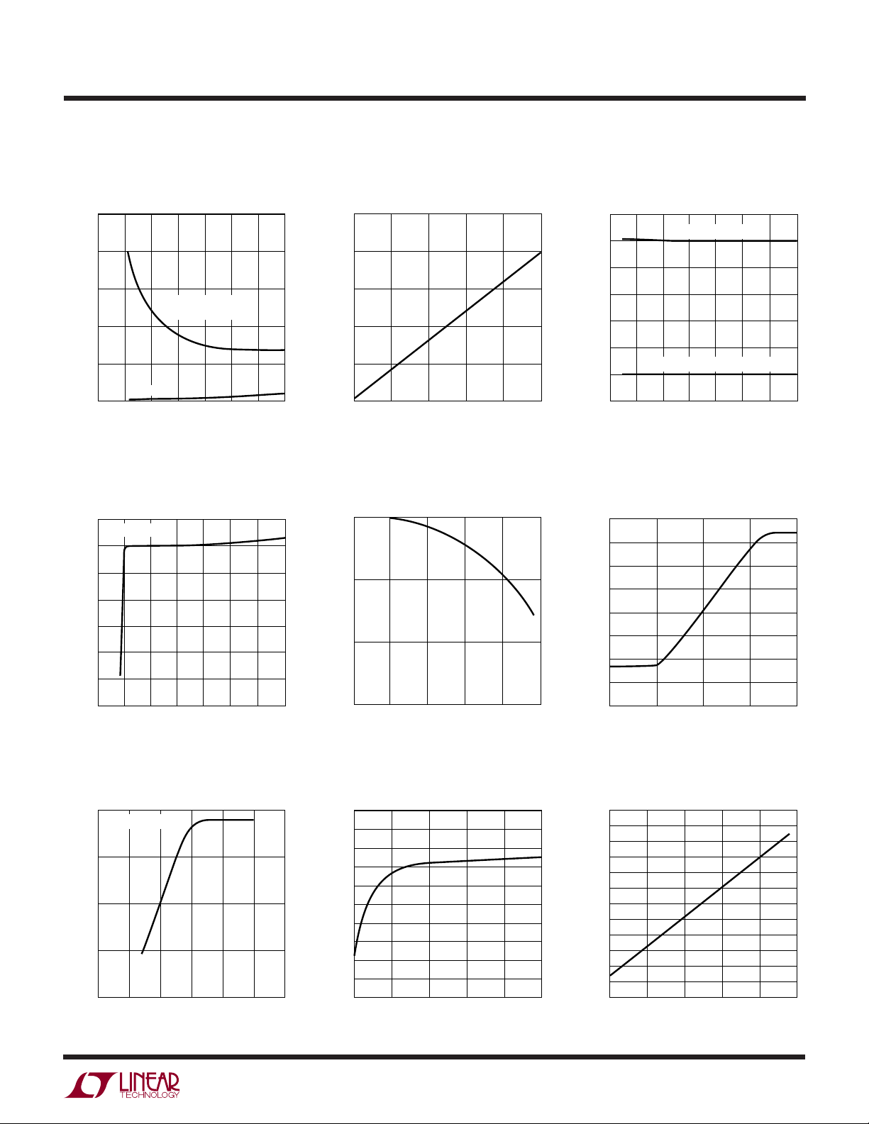
TYPICAL PERFOR A CE CHARACTERISTICS
Efficiency vs Output Current
and Mode (Figure 13)
100
Burst Mode
90
OPERATION
80
70
60
50
40
EFFICIENCY (%)
30
20
10
0
0.001
0.01
OUTPUT CURRENT (A)
FORCED
CONTINUOUS
MODE (PWM)
CONSTANT
FREQUENCY
(BURST DISABLE)
0.1
VIN = 15V
V
OUT
f = 250kHz
1
= 5V
10
3728 G01
Efficiency vs Output Current
(Figure 13)
100
90
80
70
EFFICIENCY (%)
60
50
0.001
VIN = 7V
VIN = 10V
= 15V
V
IN
V
= 20V
IN
0.01
0.1
OUTPUT CURRENT (A)
V
OUT
f = 250kHz
1
= 5V
3728 G02
Efficiency vs Input Voltage
(Figure 13)
100
90
80
70
EFFICIENCY (%)
60
50
10
5
15
INPUT VOLTAGE (V)
25
V
= 5V
OUT
= 3A
I
OUT
f = 250kHz
3728 G03
35
4
3728fc
UW
TEMPERATURE (°C)
–50
INTV
CC
AND EXTV
CC
SWITCH VOLTAGE (V)
4.95
5.00
5.05
25 75
3728 G06
4.90
4.85
–25 0
50 100 125
4.80
4.70
4.75
INTVCC VOLTAGE
EXTVCC SWITCHOVER THRESHOLD
TYPICAL PERFOR A CE CHARACTERISTICS
LTC3728
Supply Current vs Input Voltage
and Mode (Figure 13)
1000
800
600
400
SUPPLY CURRENT (µA)
200
0
05
BOTH
CONTROLLERS ON
SHUTDOWN
10
INPUT VOLTAGE (V)
20
15
Internal 5V LDO Line Regulation
5.1
I
= 1mA
LOAD
5.0
4.9
4.8
VOLTAGE (V)
4.7
CC
INTV
4.6
4.5
4.4
0
510
INPUT VOLTAGE (V)
20 30 35
15 25
INTVCC and EXTVCC Switch
EXTVCC Voltage Drop
250
200
150
100
VOLTAGE DROP (mV)
CC
EXTV
50
30
35
3728 G04
25
0
10
0
CURRENT (mA)
30
40
20
50
3728 G05
Voltage vs Temperature
Maximum Current Sense Threshold
3728 G07
Maximum Current Sense Threshold
vs Duty Factor
75
50
(mV)
SENSE
V
25
0
0
20 40 60 80
DUTY FACTOR (%)
100
3728 G08
vs Percent of Nominal Output
Voltage (Foldback)
80
70
60
50
(mV)
40
SENSE
V
30
20
10
0
0
25
PERCENT ON NOMINAL OUTPUT VOLTAGE (%)
50
75
100
3728 G09
80
60
(mV)
40
SENSE
V
20
0
Maximum Current Sense Threshold
vs V
V
SENSE(CM)
0
(Soft-Start)
RUN/SS
= 1.6V
1234
V
(V)
RUN/SS
56
3728 G10
Maximum Current Sense Threshold
vs Sense Common Mode Voltage
80
76
72
(mV)
SENSE
68
V
64
60
1
0
2
COMMON MODE VOLTAGE (V)
3
Current Sense Threshold
Voltage
vs I
TH
90
80
70
60
50
40
(mV)
30
20
SENSE
V
10
0
–10
–20
4
5
3728 G11
–30
0.5
0
1.5
2
3728 G12
3728fc
2.5
1
V
(V)
ITH
5
LTC3728
UW
TYPICAL PERFOR A CE CHARACTERISTICS
Load Regulation
0.0
–0.1
(%)
OUT
–0.2
NORMALIZED V
–0.3
–0.4
1
0
2
LOAD CURRENT (A)
Maximum Current Sense
Threshold vs Temperature
80
78
76
(mV)
SENSE
74
V
72
70
–50 –25
25
0
TEMPERATURE (°C)
V
vs V
ITH
RUN/SS
2.5
V
0
OSENSE
= 0.7V
234
1
V
RUN/SS
(V)
56
3728 G14
FCB = 0V
= 15V
V
IN
2.0
1.5
(V)
ITH
V
1.0
0.5
3
4
5
3728 G13
0
SENSE Pins Total Source Current
100
50
(µA)
0
SENSE
I
–50
–100
0
24
V
COMMON MODE VOLTAGE (V)
SENSE
6
3728 G15
Dropout Voltage vs Output Current
(Figure 14)
4
V
= 5V
OUT
3
2
R
= 0.015Ω
SENSE
DROPOUT VOLTAGE (V)
1
R
= 0.010Ω
SENSE
0
0
50
75
100
125
3728 G17
0.5 1.0 1.5 2.0
OUTPUT CURRENT (A)
2.5 3.0 3.5 4.0
3728 G18
RUN/SS Current vs Temperature
1.8
1.6
1.4
1.2
1.0
0.8
0.6
RUN/SS CURRENT (µA)
0.4
0.2
0
–50 –25
0 25 125
TEMPERATURE (°C)
75 10050
3728 G25
6
Soft-Start Up (Figure 13)
V
OUT
5V/DIV
V
RUN/SS
5V/DIV
I
L
2A/DIV
V
= 15V 5ms/DIV
IN
V
= 5V
OUT
3728 G19
V
OUT
200mV/DIV
2A/DIV
Load Step (Figure 13)
I
L
V
= 15V 20µs/DIV
IN
V
= 5V
OUT
V
= 0V
PLLFLTR
LOAD STEP = 0A TO 3A
Burst Mode OPERATION
3728 G20
V
OUT
200mV/DIV
2A/DIV
Load Step (Figure 13)
I
L
= 15V 20µs/DIV
V
IN
V
= 5V
OUT
V
= 0V
PLLFLTR
LOAD STEP = 0A TO 3A
CONTINUOUS MODE
3728 G21
3728fc
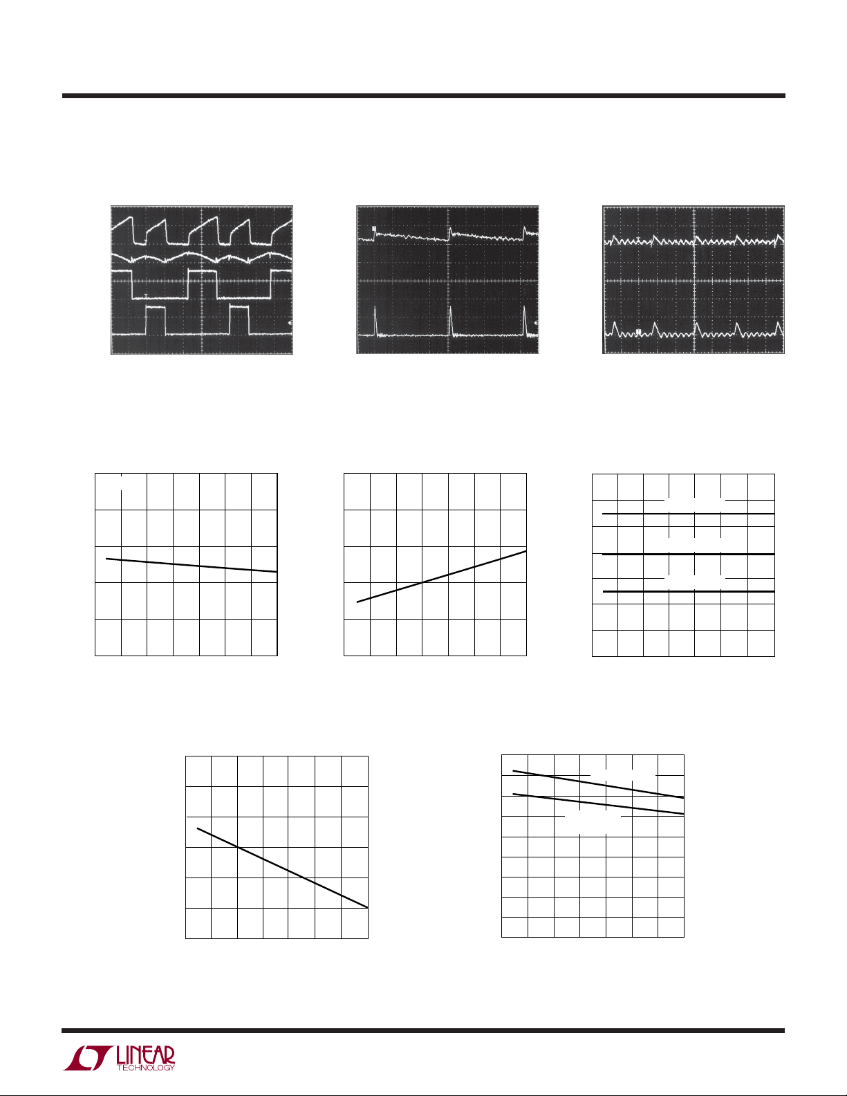
TEMPERATURE (°C)
–50
400
500
700
25 75
3728 G28
300
200
–25 0
50 100 125
100
0
600
FREQUENCY (kHz)
V
PLLFLTR
= 5V
V
PLLFLTR
= 1.2V
V
PLLFLTR
= 0V
UW
TYPICAL PERFOR A CE CHARACTERISTICS
LTC3728
Input Source/Capacitor
Instantaneous Current (Figure 13)
I
IN
2A/DIV
V
IN
200mV/DIV
V
SW1
10V/DIV
V
SW2
10V/DIV
V
= 15V 1µs/DIV
IN
V
= 5V
OUT
= 0V
V
PLLFLTR
I
= I
OUT3.3
= 2A
OUT5
Current Sense Pin Input Current
vs Temperature
35
V
= 5V
OUT
33
31
3728 G22
Burst Mode Operation (Figure 13)
V
OUT
20mV/DIV
I
L
0.5A/DIV
= 15V 10µs/DIV
V
IN
V
= 5V
OUT
= 0V
V
PLLFLTR
V
= OPEN
FCB
= 20mA
I
OUT
EXTVCC Switch Resistance
vs Temperature
10
8
6
3728 G23
Constant Frequency (Burst Inhibit)
Operation (Figure 13)
V
OUT
20mV/DIV
I
L
0.5A/DIV
= 15V 2µs/DIV
V
IN
V
= 5V
OUT
= 0V
V
PLLFLTR
V
= 5V
FCB
= 20mA
I
OUT
Oscillator Frequency
vs Temperature
3728 G24
CURRENT SENSE INPUT CURRENT (µA)
29
27
25
–50 –25
0
TEMPERATURE (°C)
50
25
75
100
Undervoltage Lockout
vs Temperature
3.50
3.45
3.40
3.35
3.30
UNDERVOLTAGE LOCKOUT (V)
3.25
3.20
–50
–25 0
TEMPERATURE (°C)
125
3728 G26
50 100 125
25 75
SWITCH RESISTANCE (Ω)
CC
EXTV
4
2
0
–50 –25
3728 G29
50
25
0
TEMPERATURE (°C)
100
125
3728 G27
75
Shutdown Latch Thresholds
vs Temperature
4.5
4.0
3.5
3.0
2.5
2.0
1.5
1.0
0.5
SHUTDOWN LATCH THRESHOLDS (V)
0
–50 –25
LATCH ARMING
LATCHOFF
THRESHOLD
0 25 125
TEMPERATURE (°C)
75 10050
3728 G30
3728fc
7

LTC3728
U
PI FU CTIO S
UU
G Package/UH Package
RUN/SS1, RUN/SS2 (Pins 1, 15/Pins 28, 13): Combina-
tion of soft-start, run control inputs and short-circuit detection timers. A capacitor to ground at each of these pins sets
the ramp time to full output current. Forcing either of these
pins back below 1.0V causes the IC to shut down the
circuitry required for that particular controller. Latchoff
overcurrent protection is also invoked via this pin as described in the Applications Information section.
SENSE1
to the Differential Current Comparators. The I
and controlled offsets between the SENSE
pins in conjunction with R
+
, SENSE2+ (Pins 2, 14/Pins 30, 12): The (+) Input
pin voltage
th
–
and SENSE
set the current trip thresh-
SENSE
+
old.
SENSE1
–
, SENSE2– (Pins 3, 13/Pins 31, 11): The (–) Input
to the Differential Current Comparators.
V
OSENSE1
, V
OSENSE2
(Pins 4, 12/Pins 1, 9): Receives the
remotely-sensed feedback voltage for each controller from
an external resistive divider across the output.
PLLFLTR (Pin 5/Pin 2): The Phase-Locked Loop’s Lowpass Filter is Tied to This Pin. Alternatively, this pin can be
driven with an AC or DC voltage source to vary the frequency of the internal oscillator.
PLLIN (Pin 6/Pin 3): External Synchronization Input to Phase
Detector. This pin is internally terminated to SGND with
50kΩ. The phase-locked loop will force the rising top gate
signal of controller 1 to be synchronized with the rising
edge of the PLLIN signal.
FCB (Pin 7/Pin 4): Forced Continuous Control Input. This
input acts on both controllers and is normally used to
regulate a secondary winding. Pulling this pin below 0.8V
will force continuous synchronous operation.
I
TH1, ITH2
(Pins 8, 11/Pins 5, 8): Error Amplifier Output and
Switching Regulator Compensation Point. Each associated
channels’ current comparator trip point increases with this
control voltage.
SGND (Pin 9/Pin 6): Small Signal Ground common to
both controllers, must be routed separately from high
current grounds to the common (–) terminals of the
C
capacitors.
OUT
3.3V
(Pin 10/Pin 7): Output of a linear regulator capable
OUT
of supplying 10mA DC with peak currents as high as 50mA.
NC (Pins 10, 16, 29, 32 UH Package Only): No Connect.
PGND (Pin 20/Pin 19): Driver Power Ground. Connects to the
sources of bottom (synchronous) N-channel MOSFETs, anodes of the Schottky rectifiers and the (–) terminal(s) of C
INTV
Dropout Regulator and the EXTV
(Pin 21/Pin 20): Output of the Internal 5V Linear Low
CC
Switch. The driver and
CC
IN
.
control circuits are powered from this voltage source. Must
be decoupled to power ground with a minimum of 4.7µF
tantalum or other low ESR capacitor.
EXTV
Internal Switch Connected to INTV
and supplies V
out regulator, whenever EXTV
EXTV
(Pin 22/Pin 21): External Power Input to an
CC
. This switch closes
CC
power, bypassing the internal low drop-
CC
is higher than 4.7V. See
CC
connection in Applications section. Do not exceed
CC
7V on this pin.
BG1, BG2 (Pins 23, 19/Pins 22, 18): High Current Gate
Drives for Bottom (Synchronous) N-Channel MOSFETs.
Voltage swing at these pins is from ground to INTV
V
(Pin 24/Pin 23): Main Supply Pin. A bypass capacitor
IN
CC
.
should be tied between this pin and the signal ground pin.
BOOST1, BOOST2 (Pins 25, 18/Pins 24, 17): Bootstrapped
Supplies to the Top Side Floating Drivers. Capacitors are
connected between the boost and switch pins and Schottky diodes are tied between the boost and INTV
Voltage swing at the boost pins is from INTV
INTV
CC
).
CC
pins.
CC
to (VIN +
SW1, SW2 (Pins 26, 17/Pins 25, 15): Switch Node
Connections to Inductors. Voltage swing at these pins is
from a Schottky diode (external) voltage drop below
ground to V
IN
.
TG1, TG2 (Pins 27, 16/Pins 26, 14): High Current Gate
Drives for Top N-Channel MOSFETs. These are the outputs
of floating drivers with a voltage swing equal to INTV
CC
–
0.5V superimposed on the switch node voltage SW.
PGOOD (Pin 28/Pin 27): Open-Drain Logic Output. PGOOD
is pulled to ground when the voltage on either V
OSENSE
pin
is not within ±7.5% of its set point.
Exposed Pad (Pin 33) SGND: The exposed pad must be
soldered to PCB ground for elecrical contact and rated
thermal performance.
8
3728fc

LTC3728
U
U
W
FU CTIO AL DIAGRA
PLLIN
F
IN
PLLFLTR
R
LP
C
LP
PGOOD
V
SEC
R6
FCB
R5
3.3V
V
IN
V
IN
EXTV
INTV
5V
+
SGND
50k
0.18µA
OUT
CC
CC
PHASE DET
OSCILLATOR
1.5V
+
–
4.7V
4.5V
0.8V
CLK1
CLK2
–
0.86V
+
V
OSENSE1
–
+
0.74V
0.86V
–
+
V
OSENSE2
–
+
0.74V
–
BINH
+
+
FCB
–
V
REF
+
–
5V
LDO
REG
INTERNAL
SUPPLY
DUPLICATE FOR SECOND
CONTROLLER CHANNEL
0.86V
4(VFB)
SLOPE
COMP
1.2µA
6V
DROP
OUT
DET
BOT
FCB
45k
+
–
+– –+
SHDN
4(VFB)
RST
B
3mV
TOP ON
SHDN
START
–
+
45k
OV
RUN
SOFT
2.4V
SRQ
Q
0.55V
I1 I2
+
–
SWITCH
EA
LOGIC
–
+
+
–
INTV
BOOST
CC
INTV
30k
30k
CC
TG
SW
BG
PGND
SENSE
SENSE
V
OSENSE
I
TH
RUN/SS
+
–
TOP
BOT
INTV
V
FB
0.80V
0.86V
V
CC
IN
D
B
C
B
D
SEC
R2
R1
C
C
C
C2
C
SS
+
C
1
SENSE
IN
C
OUT
+
V
OUT
+
C
SEC
D
R
R
C
Figure 2
U
OPERATIO
Main Control Loop
The LTC3728 uses a constant frequency, current mode
step-down architecture with the two controller channels
operating 180 degrees out of phase. During normal operation, each top MOSFET is turned on when the clock for that
channel sets the RS latch, and turned off when the main
current comparator, I1, resets the RS latch. The peak
(Refer to Functional Diagram)
3728 FD/F02
inductor current at which I1 resets the RS latch is controlled by the voltage on the I
each error amplifier EA. The V
pin, which is the output of
TH
OSENSE
pin receives the
voltage feedback signal, which is compared to the internal
reference voltage by the EA. When the load current increases, it causes a slight decrease in V
OSENSE
the 0.8V reference, which in turn causes the I
relative to
voltage to
TH
3728fc
9

LTC3728
OPERATIO
U
(Refer to Functional Diagram)
increase until the average inductor current matches the
new load current. After the top MOSFET has turned off, the
bottom MOSFET is turned on until either the inductor
current starts to reverse, as indicated by current comparator I
, or the beginning of the next cycle.
2
The top MOSFET drivers are biased from floating bootstrap capacitor C
, which normally is recharged during
B
each off cycle through an external diode when the top
MOSFET turns off. As V
, the loop may enter dropout and attempt to turn on
V
OUT
decreases to a voltage close to
IN
the top MOSFET continuously. The dropout detector detects this and forces the top MOSFET off for about 400ns
every tenth cycle to allow C
to recharge.
B
The main control loop is shut down by pulling the RUN/SS
pin low. Releasing RUN/SS allows an internal 1.2µA
current source to charge soft-start capacitor CSS. When
C
reaches 1.5V, the main control loop is enabled with the
SS
voltage clamped at approximately 30% of its maximum
I
TH
value. As C
continues to charge, the I
SS
pin voltage is
TH
gradually released allowing normal, full-current operation. When both RUN/SS1 and RUN/SS2 are low, all
LTC3728 controller functions are shut down,
including the 5V and 3.3V regulators.
Low Current Operation
The FCB pin is a multifunction pin providing two functions: 1) to provide regulation for a secondary winding by
temporarily forcing continuous PWM operation on
both controllers; and 2) select between
two
modes of low
current operation. When the FCB pin voltage is below
0.8V, the controller forces continuous PWM current
mode operation. In this mode, the top and bottom
MOSFETs are alternately turned on to maintain the output
voltage independent of direction of inductor current.
When the FCB pin is below V
INTVCC
– 1V but greater than
0.8V, the controller enters Burst Mode operation. Burst
Mode operation sets a minimum output current level
before inhibiting the top switch and turns off the synchronous MOSFET(s) when the inductor current goes negative. This combination of requirements will, at low currents, force the ITH pin below a voltage threshold that will
temporarily inhibit turn-on of both output MOSFETs until
the output voltage drops. There is 60mV of hysteresis in
the burst comparator B tied to the I
pin. This hysteresis
TH
produces output signals to the MOSFETs that turn them
on for several cycles, followed by a variable “sleep”
interval depending upon the load current. The resultant
output voltage ripple is held to a very small value by
having the hysteretic comparator after the error amplifier
gain block.
Frequency Synchronization
The phase-locked loop allows the internal oscillator to be
synchronized to an external source via the PLLIN pin. The
output of the phase detector at the PLLFLTR pin is also the
DC frequency control input of the oscillator that operates
over a 250kHz to 550kHz range corresponding to a DC
voltage input from 0V to 2.4V. When locked, the PLL aligns
the turn on of the top MOSFET to the rising edge of the
synchronizing signal. When PLLIN is left open, the PLLFLTR
pin goes low, forcing the oscillator to minimum frequency.
Constant Frequency Operation
When the FCB pin is tied to INTV
, Burst Mode operation
CC
is disabled and the forced minimum output current
requirement is removed. This provides constant frequency,
discontinuous (preventing reverse inductor current)
current operation over the widest possible output current
range. This constant frequency operation is not as efficient
as Burst Mode operation, but does provide a lower noise,
constant frequency operating mode down to approximately 1% of designed maximum output current.
Continuous Current (PWM) Operation
Tying the FCB pin to ground will force continuous current
operation. This is the least efficient operating mode, but
may be desirable in certain applications. The output can
source or sink current in this mode. When sinking current
while in forced continuous operation, current will be
forced back into the main power supply.
10
3728fc

OPERATIO
LTC3728
U
(Refer to Functional Diagram)
INTVCC/EXTVCC Power
Power for the top and bottom MOSFET drivers and most
other internal circuitry is derived from the INTV
When the EXTV
dropout linear regulator supplies INTV
is taken above 4.7V, the 5V regulator is turned off and an
internal switch is turned on connecting EXTV
This allows the INTV
efficiency external source such as the output of the regulator itself or a secondary winding, as described in the
Applications Information section.
Output Overvoltage Protection
An overvoltage comparator, OV, guards against transient
overshoots (>7.5%) as well as other more serious conditions that may overvoltage the output. In this case, the top
MOSFET is turned off and the bottom MOSFET is turned on
until the overvoltage condition is cleared.
Power Good (PGOOD) Pin
The PGOOD pin is connected to an open drain of an internal
MOSFET. The MOSFET turns on and pulls the pin low when
either output is not within ± 7.5% of the nominal output
level as determined by the resistive feedback divider.
When both outputs meet the ± 7.5% requirement, the
MOSFET is turned off within 10µs and the pin is allowed to
be pulled up by an external resistor to a source of up to 7V.
Foldback Current, Short-Circuit Detection
and Short-Circuit Latchoff
The RUN/SS capacitors are used initially to limit the inrush
current of each switching regulator. After the controller
has been started and been given adequate time to charge
up the output capacitors and provide full load current, the
RUN/SS capacitor is used in a short-circuit time-out
circuit. If the output voltage falls to less than 70% of its
nominal output voltage, the RUN/SS capacitor begins
discharging on the assumption that the output is in an
overcurrent and/or short-circuit condition. If the condition lasts for a long enough period as determined by the
size of the RUN/SS capacitor, the controller will be shut
down until the RUN/SS pin(s) voltage(s) are recycled.
pin is left open, an internal 5V low
CC
power. If EXTV
CC
to INTVCC.
CC
power to be derived from a high
CC
CC
pin.
CC
This built-in latchoff can be overridden by providing a
>5µA pull-up at a compliance of 5V to the RUN/SS pin(s).
This current shortens the soft start period but also prevents net discharge of the RUN/SS capacitor(s) during an
overcurrent and/or short-circuit condition. Foldback current limiting is also activated when the output voltage falls
below 70% of its nominal level whether or not the shortcircuit latchoff circuit is enabled. Even if a short is present
and the short-circuit latchoff is not enabled, a safe, low
output current is provided due to internal current foldback
and actual power wasted is low due to the efficient nature
of the current mode switching regulator.
THEORY AND BENEFITS OF 2-PHASE OPERATION
The LTC1628 and the LTC3728 dual high efficiency DC/DC
controllers bring the considerable benefits of 2-phase
operation to portable applications for the first time. Notebook computers, PDAs, handheld terminals and automotive electronics will all benefit from the lower input filtering
requirement, reduced electromagnetic interference (EMI)
and increased efficiency associated with 2-phase operation.
Why the need for 2-phase operation? Up until the 2-phase
family, constant-frequency dual switching regulators operated both channels in phase (i.e., single-phase operation). This means that both switches turned on at the same
time, causing current pulses of up to twice the amplitude
of those for one regulator to be drawn from the input
capacitor and battery. These large amplitude current pulses
increased the total RMS current flowing from the input
capacitor, requiring the use of more expensive input
capacitors and increasing both EMI and losses in the input
capacitor and battery.
With 2-phase operation, the two channels of the dualswitching regulator are operated 180 degrees out of
phase. This effectively interleaves the current pulses
drawn by the switches, greatly reducing the overlap time
where they add together.
The result is a significant reduction in total RMS input current, which in turn allows less
expen
sive input capacitors to be used, reduces shielding
requirements for EMI and improves real world operating
efficiency.
3728fc
11

LTC3728
OPERATIO
Figure 3. Input Waveforms Comparing Single-Phase (a) and 2-Phase (b) Operation for Dual Switching Regulators
Converting 12V to 5V and 3.3V at 3A Each. The Reduced Input Ripple with the LTC1628 2-Phase Regulator Allows
Less Expensive Input Capacitors, Reduces Shielding Requirements for EMI and Improves Efficiency
U
(Refer to Functional Diagram)
I
= 2.53A
IN(MEAS)
RMS
(a)
DC236 F03a
5V SWITCH
20V/DIV
3.3V SWITCH
20V/DIV
INPUT CURRENT
5A/DIV
INPUT VOLTAGE
500mV/DIV
I
IN(MEAS)
= 1.55A
(b)
DC236 F03b
RMS
Figure 3 compares the input waveforms for a representative single-phase dual switching regulator to the LTC1628
2-phase dual switching regulator. An actual measurement
of the RMS input current under these conditions shows
that 2-phase operation dropped the input current from
2.53A
RMS
to 1.55A
. While this is an impressive reduc-
RMS
tion in itself, remember that the power losses are propor-
2
tional to I
, meaning that the actual power wasted is
RMS
reduced by a factor of 2.66. The reduced input ripple
voltage also means less power is lost in the input power
path, which could include batteries, switches, trace/connector resistances and protection circuitry. Improvements
in both conducted and radiated EMI also directly accrue as
a result of the reduced RMS input current and voltage.
Of course, the improvement afforded by 2-phase operation is a function of the dual switching regulator’s relative
duty cycles which, in turn, are dependent upon the input
voltage V
(Duty Cycle = V
IN
OUT/VIN
). Figure 4 shows how
the RMS input current varies for single-phase and 2-phase
operation for 3.3V and 5V regulators over a wide input
voltage range.
It can readily be seen that the advantages of 2-phase
operation are not just limited to a narrow operating range,
but in fact extend over a wide region. A good rule of thumb
for most applications is that 2-phase operation will reduce
the input capacitor requirement to that for just one channel
operating at maximum current and 50% duty cycle.
A final question: If 2-phase operation offers such an
advantage over single-phase operation for dual switching
regulators, why hasn’t it been done before? The answer is
that, while simple in concept, it is hard to implement.
Constant-frequency current mode switching regulators
require an oscillator derived “slope compensation” signal
to allow stable operation of each regulator at over 50%
duty cycle. This signal is relatively easy to derive in singlephase dual switching regulators, but required the development of a new and proprietary technique to allow 2-phase
operation. In addition, isolation between the two channels
becomes more critical with 2-phase operation because
switch transitions in one channel could potentially disrupt
the operation of the other channel.
These 2-phase parts are proof that these hurdles have
been surmounted. They offer unique advantages for the
ever-expanding number of high efficiency power supplies
required in portable electronics.
3.0
SINGLE PHASE
2.5
2.0
1.5
1.0
INPUT RMS CURRENT (A)
0.5
VO1 = 5V/3A
= 3.3V/3A
V
O2
0
0
Figure 4. RMS Input Current Comparison
DUAL CONTROLLER
2-PHASE
DUAL CONTROLLER
10 20 30 40
INPUT VOLTAGE (V)
3728 F04
3728fc
12

WUUU
APPLICATIO S I FOR ATIO
LTC3728
Figure 1 on the first page is a basic LTC3728 application
circuit. External component selection is driven by the
load requirement, and begins with the selection of R
SENSE
and the inductor value. Next, the power MOSFETs and D1
are selected. Finally, C
and C
IN
are selected. The
OUT
circuit shown in Figure 1 can be configured for operation
up to an input voltage of 28V (limited by the external
MOSFETs).
R
R
Selection For Output Current
SENSE
is chosen based on the required output current.
SENSE
The LTC3728 current comparator has a maximum threshold of 75mV/R
and an input common mode range of
SENSE
SGND to 1.1(INTVCC). The current comparator threshold
sets the peak of the inductor current, yielding a maximum
average output current I
equal to the peak value less
MAX
half the peak-to-peak ripple current, ∆IL.
Allowing a margin for variations in the LTC3728 and
external component values yields:
mV
R
SENSE
50
=
I
MAX
When using the controller in very low dropout conditions,
the maximum output current level will be reduced due to
the internal compensation required to meet stability criterion for buck regulators operating at greater than 50%
duty factor. A curve is provided to estimate this reducton
in peak output current level depending upon the operating
duty factor.
Operating Frequency
2.5
2.0
1.5
1.0
PLLFLTR PIN VOLTAGE (V)
0.5
0
200 250 300 350 550400 450 500
OPERATING FREQUENCY (kHz)
3728 F05
Figure 5. PLLFLTR Pin Voltage vs Frequency
is increased the gate charge losses will be higher, reducing
efficiency (see Efficiency Considerations). The maximum
switching frequency is approximately 550kHz.
Inductor Value Calculation
The operating frequency and inductor selection are interrelated in that higher operating frequencies allow the use
of smaller inductor and capacitor values. So why would
anyone ever choose to operate at lower frequencies with
larger components? The answer is efficiency. A higher
frequency generally results in lower efficiency because of
MOSFET gate charge losses. In addition to this basic
trade-off, the effect of inductor value on ripple current and
low current operation must also be considered.
The inductor value has a direct effect on ripple current. The
inductor ripple current ∆I
tance or frequency and increases with higher V
decreases with higher induc-
L
:
IN
The LTC3728 uses a constant frequency phase-lockable
architecture with the frequency determined by an internal
capacitor. This capacitor is charged by a fixed current plus
an additional current which is proportional to the voltage
applied to the PLLFLTR pin. Refer to Phase-Locked Loop
and Frequency Synchronization in the Applications Information section for additional information.
A graph for the voltage applied to the PLLFLTR pin vs
frequency is given in Figure 5. As the operating frequency
∆I
1
=
L OUT
()( )
fL
⎛
1
V
–
⎜
⎝
V
OUT
V
IN
⎞
⎟
⎠
Accepting larger values of ∆IL allows the use of low
inductances, but results in higher output voltage ripple
and greater core losses. A reasonable starting point for
setting ripple current is ∆I
=0.3(I
L
). The maximum ∆I
MAX
L
occurs at the maximum input voltage.
3728fc
13

LTC3728
WUUU
APPLICATIO S I FOR ATIO
The inductor value also has secondary effects. The transition to Burst Mode operation begins when the average
inductor current required results in a peak current below
25% of the current limit determined by R
inductor values (higher ∆I
) will cause this to occur at
L
SENSE
. Lower
lower load currents, which can cause a dip in efficiency in
the upper range of low current operation. In Burst Mode
operation, lower inductance values will cause the burst
frequency to decrease.
Inductor Core Selection
Once the value for L is known, the type of inductor must
be selected. High efficiency converters generally cannot
afford the core loss found in low cost powdered iron
cores, forcing the use of more expensive ferrite,
®
molypermalloy, or Kool Mµ
cores. Actual core loss is
independent of core size for a fixed inductor value, but it
is very dependent on inductance selected. As inductance
increases, core losses go down. Unfortunately, increased
inductance requires more turns of wire and therefore
copper losses will increase.
Ferrite designs have very low core loss and are preferred
at high switching frequencies, so design goals can concentrate on copper loss and preventing saturation. Ferrite
core material saturates “hard,” which means that inductance collapses abruptly when the peak design current is
exceeded. This results in an abrupt increase in inductor
ripple current and consequent output voltage ripple. Do
not allow the core to saturate!
The peak-to-peak drive levels are set by the INTV
CC
voltage. This voltage is typically 5V during start-up (see
EXTV
Pin Connection). Consequently, logic-level
CC
threshold MOSFETs must be used in most applications.
The only exception is if low input voltage is expected
< 5V); then, sub-logic level threshold MOSFETs
(V
IN
(V
BV
< 3V) should be used. Pay close attention to the
GS(TH)
specification for the MOSFETs as well; most of the
DSS
logic level MOSFETs are limited to 30V or less.
Selection criteria for the power MOSFETs include the “ON”
resistance R
, reverse transfer capacitance C
DS(ON)
RSS
,
input voltage and maximum output current. When the
LTC3728 is operating in continuous mode the duty cycles
for the top and bottom MOSFETs are given by:
V
Main SwitchDuty Cycle
Synchronous Switch Duty Cycle
OUT
=
V
IN
VV
–
IN OUT
=
V
IN
The MOSFET power dissipations at maximum output
current are given by:
P
MAIN
V
OUT
=
V
IN
2
kV I C f
IN MAX RSS
()( )( )()
2
IR
MAX DS ON
()
+
1 δ
()
()
+
Molypermalloy (from Magnetics, Inc.) is a very good, low
loss core material for toroids, but it is more expensive than
ferrite. A reasonable compromise from the same manufacturer is Kool Mµ. Toroids are very space efficient,
especially when you can use several layers of wire. Because they generally lack a bobbin, mounting is more
difficult. However, designs for surface mount are available
that do not increase the height significantly.
Power MOSFET and D1 Selection
Two external power MOSFETs must be selected for each
controller in the LTC3728: One N-channel MOSFET for the
top (main) switch, and one N-channel MOSFET for the
bottom (synchronous) switch.
14
–
VV
P
SYNC
IN OUT
=
V
IN
where δ is the temperature dependency of R
2
IR
MAX DS ON
()
+
1 δ
()
()
DS(ON)
and k
is a constant inversely related to the gate drive current.
Both MOSFETs have I
2
R losses while the topside N-channel
equation includes an additional term for transition losses,
which are highest at high input voltages. For V
< 20V the
IN
high current efficiency generally improves with larger
MOSFETs, while for VIN > 20V the transition losses rapidly
increase to the point that the use of a higher R
with lower C
Kool Mµ is a registered trademark of Magnetics, Inc.
actually provides higher efficiency. The
RSS
DS(ON)
device
3728fc

WUUU
APPLICATIO S I FOR ATIO
LTC3728
synchronous MOSFET losses are greatest at high input
voltage when the top switch duty factor is low or during a
short-circuit when the synchronous switch is on close to
100% of the period.
The term (1+δ) is generally given for a MOSFET in the form
of a normalized R
δ = 0.005/°C can be used as an approximation for low
voltage MOSFETs. C
FET characteristics. The constant k = 1.7 can be used to
estimate the contributions of the two terms in the main
switch dissipation equation.
The Schottky diode D1 shown in Figure 1 conducts during
the dead-time between the conduction of the two power
MOSFETs. This prevents the body diode of the bottom
MOSFET from turning on, storing charge during the deadtime and requiring a reverse recovery period that could
cost as much as 3% in efficiency at high VIN. A 1A to 3A
Schottky is generally a good compromise for both regions
of operation due to the relatively small average current.
Larger diodes result in additional transition losses due to
their larger junction capacitance. Schottky diodes should
be placed in parallel with the synchronous MOSFETs when
operating in pulse-skip mode or in Burst Mode operation.
vs Temperature curve, but
DS(ON)
is usually specified in the MOS-
RSS
battery currents down. 20µF to 40µF is usually sufficient
for a 25W output supply operating at 200kHz. The ESR of
the capacitor is important for capacitor power dissipation
as well as overall battery efficiency. All of the power (RMS
ripple current • ESR) not only heats up the capacitor but
wastes power from the battery.
Medium voltage (20V to 35V) ceramic, tantalum, OS-CON
and switcher-rated electrolytic capacitors can be used as
input capacitors, but each has drawbacks: ceramic voltage
coefficients are very high and may have audible piezoelectric effects; tantalums need to be surge-rated; OS-CONs
suffer from higher inductance, larger case size and limited
surface-mount applicability; electrolytics’ higher ESR and
dryout possibility require several to be used. Multiphase
systems allow the lowest amount of capacitance overall.
As little as one 22µF or two to three 10µF ceramic capaci-
tors are an ideal choice in a 20W to 35W power supply due
to their extremely low ESR. Even though the capacitance
at 20V is substantially below their rating at zero-bias, very
low ESR loss makes ceramics an ideal candidate for
highest efficiency battery operated systems. Also consider parallel ceramic and high quality electrolytic capacitors as an effective means of achieving ESR and bulk
capacitance goals.
and C
C
IN
The selection of C
tecture and its impact on the worst-case RMS current
drawn through the input network (battery/fuse/capacitor).
It can be shown that the worst case RMS current occurs
when only one controller is operating. The controller with
the highest (V
formula below to determine the maximum RMS current
requirement. Increasing the output current, drawn from
the other out-of-phase controller, will actually decrease
the input RMS ripple current from this maximum value
(see Figure 4). The out-of-phase technique typically reduces the input capacitor’s RMS ripple current by a factor
of 30% to 70% when compared to a single phase power
supply solution.
The type of input capacitor, value and ESR rating have
efficiency effects that need to be considered in the selection process. The capacitance value chosen should be
sufficient to store adequate charge to keep high peak
Selection
OUT
OUT
is simplified by the multiphase archi-
IN
)(I
) product needs to be used in the
OUT
In continuous mode, the source current of the top N-channel MOSFET is a square wave of duty cycle V
prevent large voltage transients, a low ESR input capacitor
sized for the maximum RMS current of one channel must
be used. The maximum RMS capacitor current is given by:
VVV
()
[]
C quiredI I
Re
IN RMS MAX
This formula has a maximum at VIN = 2V
I
= I
RMS
monly used for design because even significant deviations
do not offer much relief. Note that capacitor manufacturer’s
ripple current ratings are often based on only 2000 hours
of life. This makes it advisable to further derate the
capacitor, or to choose a capacitor rated at a higher
temperature than required. Several capacitors may also be
paralleled to meet size or height requirements in the
design. Always consult the manufacturer if there is any
question.
/2. This simple worst case condition is com-
OUT
≈
OUT IN OUT
OUT/VIN
−
V
IN
OUT
. To
/
12
, where
3728fc
15

LTC3728
WUUU
APPLICATIO S I FOR ATIO
The benefit of the LTC3728 multiphase can be calculated
by using the equation above for the higher power controller and then calculating the loss that would have resulted
if both controller channels switch on at the same time. The
total RMS power lost is lower when both controllers are
operating due to the interleaving of current pulses through
the input capacitor’s ESR. This is why the input capacitor’s
requirement calculated above for the worst-case controller is adequate for the dual controller design. Remember
that input protection fuse resistance, battery resistance
and PC board trace resistance losses are also reduced due
to the reduced peak currents in a multiphase system.
The
overall benefit of a multiphase design will only be fully
realized when the source impedance of the power supply/
battery is included in the efficiency testing.
The drains of
the two top MOSFETS should be placed within 1cm of each
other and share a common C
and C
resonances at V
The selection of C
may produce undesirable voltage and current
IN
.
IN
is driven by the required effective
OUT
(s). Separating the drains
IN
series resistance (ESR). Typically once the ESR requirement is satisfied the capacitance is adequate for filtering.
The output ripple (∆V
⎛
∆∆V I ESR
≈ +
OUT L
⎜
⎝
Where f = operating frequency, C
and ∆I
= ripple current in the inductor. The output ripple
L
is highest at maximum input voltage since ∆I
with input voltage. With ∆I
ripple will typically be less than 50mV at max V
) is determined by:
OUT
⎞
1
OUT
= 0.3I
L
⎟
⎠
= output capacitance,
OUT
8
fC
OUT(MAX)
increases
L
the output
assum-
IN
ing:
Recommended ESR < 2 R
C
OUT
and C
> 1/(8fR
OUT
SENSE
)
SENSE
The first condition relates to the ripple current into the
ESR of the output capacitance while the second term
guarantees that the output capacitance does not significantly discharge during the operating frequency period
due to ripple current. The choice of using smaller output
capacitance increases the ripple voltage due to the discharging term but can be compensated for by using
capacitors of very low ESR to maintain the ripple voltage
at or below 50mV. The I
pin OPTI-LOOP compensation
TH
components can be optimized to provide stable, high
performance transient response regardless of the output
capacitors selected.
Manufacturers such as Nichicon, United Chemicon and
Sanyo can be considered for high performance throughhole capacitors. The OS-CON semiconductor dielectric
capacitor available from Sanyo has the lowest (ESR)(size)
product of any aluminum electrolytic at a somewhat
higher price. An additional ceramic capacitor in parallel
with OS-CON capacitors is recommended to reduce the
inductance effects.
In surface mount applications multiple capacitors may
need to be used in parallel to meet the ESR, RMS current
handling and load step requirements of the application.
Aluminum electrolytic, dry tantalum and special polymer
capacitors are available in surface mount packages. Special polymer surface mount capacitors offer very low ESR
but have lower storage capacity per unit volume than other
capacitor types. These capacitors offer a very cost-effective output capacitor solution and are an ideal choice when
combined with a controller having high loop bandwidth.
Tantalum capacitors offer the highest capacitance density
and are often used as output capacitors for switching
regulators having controlled soft-start. Several excellent
surge-tested choices are the AVX TPS, AVX TPSV or the
KEMET T510 series of surface mount tantalums, available
in case heights ranging from 2mm to 4mm. Aluminum
electrolytic capacitors can be used in cost-driven applications providing that consideration is given to ripple current
ratings, temperature and long term reliability. A typical
application will require several to many aluminum electrolytic capacitors in parallel. A combination of the above
mentioned capacitors will often result in maximizing performance and minimizing overall cost. Other capacitor
types include Nichicon PL series, NEC Neocap, Cornell
Dubilier ESRE and Sprague 595D series. Consult manufacturers for other specific recommendations.
16
3728fc

WUUU
APPLICATIO S I FOR ATIO
LTC3728
INTVCC Regulator
An internal P-channel low dropout regulator produces 5V
at the INTV
pin from the VIN supply pin. INTVCC powers
CC
the drivers and internal circuitry within the LTC3728. The
INTV
pin regulator can supply a peak current of 50mA
CC
and must be bypassed to ground with a minimum of
4.7µF tantalum, 10µF special polymer, or low ESR type
electrolytic capacitor. A 1µF ceramic capacitor placed
directly adjacent to the INTV
and PGND IC pins is highly
CC
recommended. Good bypassing is necessary to supply
the high transient currents required by the MOSFET gate
drivers and to prevent interaction between channels.
Higher input voltage applications in which large MOSFETs
are being driven at high frequencies may cause the maximum junction temperature rating for the LTC3728 to be
exceeded. The system supply current is normally dominated by the gate charge current. Additional external
loading of the INTV
and 3.3V linear regulators also
CC
needs to be taken into account for the power dissipation
calculations. The total INTV
either the 5V internal linear regulator or by the EXTV
current can be supplied by
CC
CC
input pin. When the voltage applied to the EXTVCC pin is
less than 4.7V, all of the INTV
current is supplied by the
CC
internal 5V linear regulator. Power dissipation for the IC in
this case is highest: (V
IN
)(I
), and overall efficiency
INTVCC
is lowered. The gate charge current is dependent on
operating frequency as discussed in the Efficiency Considerations section. The junction temperature can be estimated by using the equations given in Note 2 of the
Electrical Characteristics. For example, the LTC3728 V
IN
current is limited to less than 24mA from a 24V supply
when not using the EXTV
= 70°C + (24mA)(24V)(95°C/W) = 125°C
T
J
pin as follows:
CC
Use of the EXTVCC input pin reduces the junction temperature to:
T
= 70°C + (24mA)(5V)(95°C/W) = 81°C
J
Dissipation should be calculated to also include any added
current drawn from the internal 3.3V linear regulator. To
prevent maximum junction temperature from being
exceeded, the input supply current must be checked
operating in continuous mode at maximum V
IN
.
EXTV
Connection
CC
The LTC3728 contains an internal P-channel MOSFET
switch connected between the EXTV
When the voltage applied to EXTV
and INTVCC pins.
CC
rises above 4.7V, the
CC
internal regulator is turned off and the switch closes,
connecting the EXTV
pin to the INTV
CC
pin thereby
CC
supplying internal power. The switch remains closed as
long as the voltage applied to EXTV
remains above 4.5V.
CC
This allows the MOSFET driver and control power to be
derived from the output during normal operation (4.7V <
V
< 7V) and from the internal regulator when the output
OUT
is out of regulation (start-up, short-circuit). If more
current is required through the EXTV
switch than is
CC
specified, an external Schottky diode can be added between the EXTV
than 7V to the EXTV
and INTVCC pins. Do not apply greater
CC
pin and ensure that EXTVCC<VIN.
CC
Significant efficiency gains can be realized by powering
INTV
from the output, since the VIN current resulting
CC
from the driver and control currents will be scaled by a
factor of (Duty Cycle)/(Efficiency). For 5V regulators this
supply means connecting the EXTVCC pin directly to V
OUT
.
However, for 3.3V and other lower voltage regulators,
additional circuitry is required to derive INTV
power
CC
from the output.
The following list summarizes the four possible connections for EXTV
1. EXTVCC Left Open (or Grounded). This will cause INTV
CC:
CC
to be powered from the internal 5V regulator resulting in
an efficiency penalty of up to 10% at high input voltages.
2. EXTV
Connected directly to V
CC
. This is the normal
OUT
connection for a 5V regulator and provides the highest
efficiency.
3. EXTVCC Connected to an External supply. If an external
supply is available in the 5V to 7V range, it may be used to
power EXTV
providing it is compatible with the MOSFET
CC
gate drive requirements.
4. EXTV
Connected to an Output-Derived Boost Net-
CC
work. For 3.3V and other low voltage regulators, efficiency
gains can still be realized by connecting EXTVCC to an
output-derived voltage that has been boosted to greater
than 4.7V. This can be done with either the inductive boost
3728fc
17

LTC3728
EXTV
CC
V
IN
TG1
SW
BG1
PGND
LTC3728
R
SENSE
V
OUT
VN2222LL
+
C
OUT
3728 F06b
N-CH
N-CH
+
C
IN
+
1µF
V
IN
L1
BAT85 BAT85
BAT85
0.22µF
WUUU
APPLICATIO S I FOR ATIO
winding as shown in Figure 6a or the capacitive charge
pump shown in Figure 6b. The charge pump has the
advantage of simple magnetics.
Topside MOSFET Driver Supply (CB, DB)
External bootstrap capacitors C
connected to the BOOST
B
pins supply the gate drive voltages for the topside MOSFETs.
Capacitor C
external diode D
in the functional diagram is charged though
B
from INTVCC when the SW pin is low.
B
When one of the topside MOSFETs is to be turned on, the
driver places the C
voltage across the gate-source of the
B
desired MOSFET. This enhances the MOSFET and turns on
the topside switch. The switch node voltage, SW, rises to
V
and the BOOST pin follows. With the topside MOSFET
IN
on, the boost voltage is above the input supply: V
V
IN
+ V
. The value of the boost capacitor CB needs
INTVCC
BOOST
=
to be 100 times that of the total input capacitance of the
topside MOSFET(s). The reverse breakdown of the external Schottky diode must be greater than V
IN(MAX)
. When
adjusting the gate drive level, the final arbiter is the total
input current for the regulator. If a change is made and the
input current decreases, then the efficiency has improved.
If there is no change in input current, then there is no
change in efficiency.
Output Voltage
The LTC3728 output voltages are each set by an external
feedback resistive divider carefully placed across
the output capacitor. The resultant feedback signal is
compared with the internal precision 0.800V voltage
reference by the error amplifier. The output voltage is
given by the equation:
⎛
08 1
VV
OUT
.
=+
⎜
⎝
⎞
2
R
⎟
1
R
⎠
where R1 and R2 are defined in Figure 2.
SENSE
+
/SENSE– Pins
The common mode input range of the current comparator
sense pins is from 0V to (1.1)INTV
. Continuous linear
CC
operation is guaranteed throughout this range allowing
output voltage setting from 0.8V to 7.7V, depending upon
the voltage applied to EXTV
. A differential NPN input
CC
stage is biased with internal resistors from an internal
2.4V source as shown in the Functional Diagram. This
requires that current either be sourced or sunk from the
SENSE pins depending on the output voltage. If the output
voltage is below 2.4V current will flow out of both SENSE
pins to the main output. The output can be easily preloaded
by the V
resistive divider to compensate for the current
OUT
comparator’s negative input bias current. The maximum
current flowing out of each pair of SENSE pins is:
I
SENSE
Since V
+
+ I
OSENSE
–
SENSE
= (2.4V – V
OUT
)/24k
is servoed to the 0.8V reference voltage, we
can choose R1 in Figure 2 to have a maximum value to
absorb this current.
V
IN
IN
N-CH
N-CH
+
C
IN
R
SENSE
T1
1:N
OPTIONAL EXTV
CONNECTION
5V < V
EXTV
R6
FCB
R5
SGND
Figure 6a. Secondary Output Loop & EXTVCC Connection
CC
< 7V
SEC
LTC3728
CC
V
TG1
SW
BG1
PGND
18
V
SEC
+
1µF
V
OUT
+
C
OUT
3728 F06a
Figure 6b. Capacitive Charge Pump for EXTV
CC
3728fc

WUUU
APPLICATIO S I FOR ATIO
124
for V
=
MAX
()
< 2.4V
OUT
⎜
⎝
Rk
⎛
.
08
.–
VV
24
Regulating an output voltage of 1.8V, the maximum value
of R1 should be 32K. Note that for an output voltage above
2.4V, R1 has no maximum value necessary to absorb the
sense currents; however, R1 is still bounded by the
V
OSENSE
feedback current.
V
OUT
⎞
⎟
⎠
V
3.3V OR 5V RUN/SS
*OPTIONAL TO DEFEAT OVERCURRENT LATCHOFF
IN
RSS*
D1
C
SS
(a) (b)
Figure 7. RUN/SS Pin Interfacing
LTC3728
INTV
CC
RSS*
RUN/SS
3728 F07
C
SS
Soft-Start/Run Function
The RUN/SS1 and RUN/SS2 pins are multipurpose pins
that provide a soft-start function and a means to shut
down the LTC3728. Soft-start reduces the input power
source’s surge currents by gradually increasing the
controller’s current limit (proportional to V
). This pin
ITH
can also be used for power supply sequencing.
An internal 1.2µA current source charges up the C
SS
capacitor. When the voltage on RUN/SS1 (RUN/SS2)
reaches 1.5V, the particular controller is permitted to start
operating. As the voltage on RUN/SS increases from 1.5V
to 3.0V, the internal current limit is increased from 25mV/
R
SENSE
to 75mV/R
. The output current limit ramps
SENSE
up slowly, taking an additional 1.25s/µF to reach full
current. The output current thus ramps up slowly, reducing the starting surge current required from the input
power supply. If RUN/SS has been pulled all the way to
ground there is a delay before starting of approximately:
15
.
t
DELAY SS SS
t
IRAMP SS SS
V
=
=
CsFC
12
.
A
µ
315
.
VV
−
12
.
A
µ
125
./
=µ
()
125
CsFC
./
=µ
()
By pulling both RUN/SS pins below 1V, the LTC3728 is
put into low current shutdown (IQ = 20µA). The RUN/SS
pins can be driven directly from logic as shown in Figure
7. Diode D1 in Figure 7 reduces the start delay but allows
CSS to ramp up slowly providing the soft-start function.
Each RUN/SS pin has an internal 6V zener clamp (See
Functional Diagram).
Fault Conditions: Overcurrent Latchoff
The RUN/SS pins also provide the ability to latch off the
controller(s) when an overcurrent condition is detected.
The RUN/SS capacitor, C
, is used initially to turn on and
SS
limit the inrush current. After the controller has been
started and been given adequate time to charge up the
output capacitor and provide full load current, the RUN/SS
capacitor is used for a short-circuit timer. If the regulator’s
output voltage falls to less than 70% of its nominal value
after CSS reaches 4.1V, CSS begins discharging on the
assumption that the output is in an overcurrent condition.
If the condition lasts for a long enough period as determined by the size of the CSS and the specified discharge
current, the controller will be shut down until the RUN/SS
pin voltage is recycled. If the overload occurs during startup, the time can be approximated by:
t
≈ [CSS(4.1 – 1.5 + 4.1 – 3.5)]/(1.2µA)
LO1
= 2.7 • 10
If the overload occurs after start-up the voltage on C
6
(CSS)
SS
will
begin discharging from the zener clamp voltage:
t
≈ [CSS (6 – 3.5)]/(1.2µA) = 2.1 • 106 (CSS)
LO2
This built-in overcurrent latchoff can be overridden by
providing a pull-up resistor to the RUN/SS pin as shown
in Figure 7. This resistance shortens the soft-start period
and prevents the discharge of the RUN/SS capacitor
during an over current condition. Tying this pull-up resistor to V
Diode-connecting this pull-up resistor to INTV
as in Figure 7a, defeats overcurrent latchoff.
IN
, as in
CC
Figure 7b, eliminates any extra supply current during
controller shutdown while eliminating the INTV
loading
CC
from preventing controller start-up.
3728fc
19

LTC3728
WUUU
APPLICATIO S I FOR ATIO
Why should you defeat overcurrent latchoff? During the
prototyping stage of a design, there may be a problem
with noise pickup or poor layout causing the protection
circuit to latch off. Defeating this feature will easily allow
troubleshooting of the circuit and PC layout. The internal
short-circuit and foldback current limiting still remains
active, thereby protecting the power supply system from
failure. After the design is complete, a decision can be
made whether to enable the latchoff feature.
The value of the soft-start capacitor CSS may need to be
scaled with output voltage, output capacitance and load
current characteristics. The minimum soft-start capacitance is given by:
CSS > (C
OUT
)(V
) (10–4) (R
OUT
SENSE
)
The minimum recommended soft-start capacitor of
C
= 0.1µF will be sufficient for most applications.
SS
Fault Conditions: Current Limit and Current Foldback
The LTC3728 current comparator has a maximum sense
voltage of 75mV resulting in a maximum MOSFET current
of 75mV/R
generally occurs with the largest V
. The maximum value of current limit
SENSE
at the highest ambi-
IN
ent temperature, conditions that cause the highest power
dissipation in the top MOSFET.
The LTC3728 includes current foldback to help further
limit load current when the output is shorted to ground.
The foldback circuit is active even when the overload
shutdown latch described above is overridden. If the
output falls below 70% of its nominal output level, then the
maximum sense voltage is progressively lowered from
75mV to 25mV. Under short-circuit conditions with very
low duty cycles, the LTC3728 will begin cycle skipping in
order to limit the short-circuit current. In this situation the
bottom MOSFET will be dissipating most of the power but
less than in normal operation. The short-circuit ripple
current is determined by the minimum on-time t
ON(MIN)
of
the LTC3728 (less than 200ns), the input voltage and
inductor value:
∆I
L(SC)
= t
ON(MIN)
(VIN/L)
The resulting short-circuit current is:
mV
I
25 1
=+
SC
R
SENSE
I
∆
LSC
()
2
Fault Conditions: Overvoltage Protection (Crowbar)
The overvoltage crowbar is designed to blow a system
input fuse when the output voltage of the regulator rises
much higher than nominal levels. The crowbar causes
huge currents to flow, that blow the fuse to protect against
a shorted top MOSFET if the short occurs while the
controller is operating.
A comparator monitors the output for overvoltage conditions. The comparator (OV) detects overvoltage faults
greater than 7.5% above the nominal output voltage.
When this condition is sensed, the top MOSFET is turned
off and the bottom MOSFET is turned on until the overvoltage condition is cleared. The output of this comparator is
only latched by the overvoltage condition itself and will
therefore allow a switching regulator system having a poor
PC layout to function while the design is being debugged.
The bottom MOSFET remains on continuously for as long
as the OV condition persists; if V
returns to a safe level,
OUT
normal operation automatically resumes. A shorted top
MOSFET will result in a high current condition which will
open the system fuse. The switching regulator will regulate properly with a leaky top MOSFET by altering the duty
cycle to accommodate the leakage.
Phase-Locked Loop and Frequency Synchronization
The LTC3728 has a phase-locked loop comprised of an
internal voltage controlled oscillator and phase detector.
This allows the top MOSFET turn-on to be locked to the
rising edge of an external source. The frequency range of
the voltage controlled oscillator is ±50% around the
center frequency fO. A voltage applied to the PLLFLTR pin
of 1.2V corresponds to a frequency of approximately
400kHz. The nominal operating frequency range of the
LTC3728 is 250kHz to 550kHz.
20
3728fc

WUUU
APPLICATIO S I FOR ATIO
LTC3728
The phase detector used is an edge sensitive digital type
which provides zero degrees phase shift between the
external and internal oscillators. This type of phase detector will not lock up on input frequencies close to the
harmonics of the VCO center frequency. The PLL hold-in
range, ∆f
, is equal to the capture range, ∆f
H
C:
∆fH = ∆fC = ± 0.5 fO (250kHz-550kHz)
The output of the phase detector is a complementary pair
of current sources charging or discharging the external
filter network on the PLLFLTR pin.
If the external frequency (f
lator frequency f
, current is sourced continuously,
0SC
) is greater than the oscil-
PLLIN
pulling up the PLLFLTR pin. When the external frequency
is less than f
, current is sunk continuously, pulling
0SC
down the PLLFLTR pin. If the external and internal frequencies are the same but exhibit a phase difference, the
current sources turn on for an amount of time corresponding to the phase difference. Thus the voltage on the
PLLFLTR pin is adjusted until the phase and frequency of
the external and internal oscillators are identical. At this
stable operating point the phase comparator output is
open and the filter capacitor C
holds the voltage. The
LP
LTC3728 PLLIN pin must be driven from a low impedance
source such as a logic gate located close to the pin. When
using multiple LTC3728’s (or LTC3729’s, as shown in
Figure 14) for a phase-locked system, the PLLFLTR pin of
the master oscillator should be biased at a voltage that will
guarantee the slave oscillator(s) ability to lock onto the
master’s frequency. A DC voltage of 0.7V to 1.7V applied
to the master oscillator’s PLLFLTR pin is recommended in
order to meet this requirement. The resultant operating
frequency can range from 300kHz to 470kHz.
The loop filter components (C
, RLP) smooth out the
LP
current pulses from the phase detector and provide a
stable input to the voltage controlled oscillator. The filter
components CLP and RLP determine how fast the loop
acquires lock. Typically R
=10kΩ and CLP is 0.01µF to
LP
0.1µF.
Minimum On-Time Considerations
Minimum on-time t
ON(MIN)
is the smallest time duration
that the LTC3728 is capable of turning on the top MOSFET.
It is determined by internal timing delays and the gate
charge required to turn on the top MOSFET. Low duty cycle
applications may approach this minimum on-time limit
and care should be taken to ensure that
V
t
()
ON MIN
<
Vf
OUT
IN
()
If the duty cycle falls below what can be accommodated by
the minimum on-time, the LTC3728 will begin to skip
cycles. The output voltage will continue to be regulated,
but the ripple voltage and current will increase.
The minimum on-time for the LTC3728 is approximately
100ns. However, as the peak sense voltage decreases the
minimum on-time gradually increases up to about 150ns.
This is of particular concern in forced continuous applications with low ripple current at light loads. If the duty cycle
drops below the minimum on-time limit in this situation,
a significant amount of cycle skipping can occur with
correspondingly larger current and voltage ripple.
FCB Pin Operation
The FCB pin can be used to regulate a secondary winding
or as a logic level input. Continuous operation is forced on
both controllers when the FCB pin drops below 0.8V.
During continuous mode, current flows continuously in
the transformer primary. The secondary winding(s) draw
current only when the bottom, synchronous switch is on.
When primary load currents are low and/or the V
IN/VOUT
ratio is low, the synchronous switch may not be on for a
sufficient amount of time to transfer power from the
output capacitor to the secondary load. Forced continuous
operation will support secondary windings providing there
is sufficient synchronous switch duty factor. Thus, the
FCB input pin removes the requirement that power must
be drawn from the inductor primary in order to extract
3728fc
21

LTC3728
WUUU
APPLICATIO S I FOR ATIO
power from the auxiliary windings. With the loop in
continuous mode, the auxiliary outputs may nominally be
loaded without regard to the primary output load.
The secondary output voltage V
is normally set as
SEC
shown in Figure 6a by the turns ratio N of the transformer:
≅ (N + 1) V
V
SEC
OUT
However, if the controller goes into Burst Mode operation
and halts switching due to a light primary load current,
then V
V
SEC
VV
will droop. An external resistive divider from
SEC
to the FCB pin sets a minimum voltage V
⎞
6
R
⎟
5
R
⎠
SEC MIN()
⎛
08 1
.≈ +
⎜
⎝
SEC(MIN)
:
where R5 and R6 are shown in Figure 2.
If V
temporary continuous switching operation until V
drops below this level, the FCB voltage forces
SEC
SEC
is
again above its minimum.
In order to prevent erratic operation if no external connections are made to the FCB pin, the FCB pin has a 0.18µA
internal current source pulling the pin high. Include this
current when choosing resistor values R5 and R6.
The following table summarizes the possible states available on the FCB pin:
Table 1
FCB Pin Condition
0V to 0.75V Forced Continuous Both Controllers
(Current Reversal Allowed—
Burst Inhibited)
0.85V < V
Feedback Resistors Regulating a Secondary Winding
>4.8V Burst Mode Operation Disabled
< 4.0V Minimum Peak Current Induces
FCB
Burst Mode Operation
No Current Reversal Allowed
Constant Frequency Mode Enabled
No Current Reversal Allowed
No Minimum Peak Current
Voltage Positioning
Voltage positioning can be used to minimize peak-to-peak
output voltage excursions under worst-case transient
loading conditions. The open-loop DC gain of the control
loop is reduced depending upon the maximum load step
specifications. Voltage positioning can easily be added to
the LTC3728 by loading the I
pin with a resistive divider
TH
having a Thevenin equivalent voltage source equal to the
midpoint operating voltage range of the error amplifier, or
1.2V (see Figure 8).
The resistive load reduces the DC loop gain while maintaining the linear control range of the error amplifier. The
maximum output voltage deviation can theoretically be
reduced to half or alternatively the amount of output
capacitance can be reduced for a particular application. A
complete explanation is included in Design Solutions 10.
(See www.linear-tech.com)
INTV
CC
R
T2
I
TH
R
R
Figure 8. Active Voltage Positioning
Applied to the LTC3728
C
T1
C
C
LTC3728
3728 F08
Efficiency Considerations
The percent efficiency of a switching regulator is equal to
the output power divided by the input power times 100%.
It is often useful to analyze individual losses to determine
what is limiting the efficiency and which change would
produce the most improvement. Percent efficiency can be
expressed as:
%Efficiency = 100% – (L1 + L2 + L3 + ...)
where L1, L2, etc. are the individual losses as a percentage
of input power.
Although all dissipative elements in the circuit produce
losses, four main sources usually account for most of the
losses in LTC3728 circuits: 1) LTC3728 VIN current (including loading on the 3.3V internal regulator), 2) INTV
CC
regulator current, 3) I2R losses, 4) Topside MOSFET
transition losses.
1. The V
current has two components: the first is the DC
IN
supply current given in the Electrical Characteristics table,
3728fc
22

WUUU
APPLICATIO S I FOR ATIO
LTC3728
which excludes MOSFET driver and control currents; the
second is the current drawn from the 3.3V linear regulator
output. V
2. INTV
current typically results in a small (<0.1%) loss.
IN
current is the sum of the MOSFET driver and
CC
control currents. The MOSFET driver current results from
switching the gate capacitance of the power MOSFETs.
Each time a MOSFET gate is switched from low to high to
low again, a packet of charge dQ moves from INTV
ground. The resulting dQ/dt is a current out of INTV
CC
CC
that
to
is typically much larger than the control circuit current. In
continuous mode, I
GATECHG
=f(QT+QB), where QT and Q
B
are the gate charges of the topside and bottom side
MOSFETs.
Supplying INTV
from an output-derived source will scale the V
power through the EXTVCC switch input
CC
current
IN
required for the driver and control circuits by a factor of
(Duty Cycle)/(Efficiency). For example, in a 20V to 5V
application, 10mA of INTVCC current results in approximately 2.5mA of V
current. This reduces the mid-current
IN
loss from 10% or more (if the driver was powered directly
from V
3. I
) to only a few percent.
IN
2
R losses are predicted from the DC resistances of the
fuse (if used), MOSFET, inductor, current sense resistor,
and input and output capacitor ESR. In continuous mode
the average output current flows through L and R
SENSE
,
but is “chopped” between the topside MOSFET and the
synchronous MOSFET. If the two MOSFETs have approximately the same R
, then the resistance of one
DS(ON)
MOSFET can simply be summed with the resistances of L,
R
R
and ESR to obtain I2R losses. For example, if each
SENSE
= 30mΩ, RL = 50mΩ, R
DS(ON)
= 10mΩ and R
SENSE
ESR
= 40mΩ (sum of both input and output capacitance
losses), then the total resistance is 130mΩ. This results in
losses ranging from 3% to 13% as the output current
increases from 1A to 5A for a 5V output, or a 4% to 20%
loss for a 3.3V output. Efficiency varies as the inverse
square of V
for the same external components and
OUT
output power level. The combined effects of increasingly
lower output voltages and higher currents required by
high performance digital systems is not doubling but
quadrupling the importance of loss terms in the switching
regulator system!
4. Transition losses apply only to the topside MOSFET(s),
and become significant only when operating at high input
voltages (typically 15V or greater). Transition losses can
be estimated from:
Transition Loss = (1.7) V
2
I
IN
O(MAX) CRSS
f
Other “hidden” losses such as copper trace and internal
battery resistances can account for an additional 5% to
10% efficiency degradation in portable systems. It is very
important to include these “system” level losses during
the design phase. The internal battery and fuse resistance
losses can be minimized by making sure that CIN has
adequate charge storage and very low ESR at the switching frequency. A 25W supply will typically require a minimum of 20µF to 40µF of capacitance having a maximum
of 20mΩ to 50mΩ of ESR. The LTC3728 2-phase architecture typically halves this input capacitance requirement
over competing solutions. Other losses including Schottky
conduction losses during dead-time and inductor core
losses generally account for less than 2% total additional
loss.
Checking Transient Response
The regulator loop response can be checked by looking at
the load current transient response. Switching regulators
take several cycles to respond to a step in DC (resistive)
load current. When a load step occurs, V
amount equal to ∆I
series resistance of C
discharge C
generating the feedback error signal that
OUT
(ESR), where ESR is the effective
LOAD
OUT
. ∆I
also begins to charge or
LOAD
shifts by an
OUT
forces the regulator to adapt to the current change and
return V
time V
to its steady-state value. During this recovery
OUT
can be monitored for excessive overshoot or
OUT
ringing, which would indicate a stability problem. OPTILOOP compensation allows the transient response to be
optimized over a wide range of output capacitance and
ESR values.
The availability of the ITH pin not only allows
optimization of control loop behavior but also provides a
DC coupled and AC filtered closed loop response test
point. The DC step, rise time and settling at this test point
truly reflects the closed loop response
. Assuming a predominantly second order system, phase margin and/or
damping factor can be estimated using the percentage of
3728fc
23

LTC3728
WUUU
APPLICATIO S I FOR ATIO
overshoot seen at this pin. The bandwidth can also be
estimated by examining the rise time at the pin. The I
TH
external components shown in the Figure 1 circuit will
provide an adequate starting point for most applications.
The I
series RC-CC filter sets the dominant pole-zero
TH
loop compensation. The values can be modified slightly
(from 0.5 to 2 times their suggested values) to optimize
transient response once the final PC layout is done and the
particular output capacitor type and value have been
determined. The output capacitors need to be selected
because the various types and values determine the loop
gain and phase. An output current pulse of 20% to 80% of
full-load current having a rise time of 1µs to 10µs will
produce output voltage and ITH pin waveforms that will
give a sense of the overall loop stability without breaking
the feedback loop. Placing a power MOSFET directly
across the output capacitor and driving the gate with an
appropriate signal generator is a practical way to produce
a realistic load step condition. The initial output voltage
step resulting from the step change in output current may
not be within the bandwidth of the feedback loop, so this
signal cannot be used to determine phase margin. This is
why it is better to look at the ITH pin signal which is in the
feedback loop and is the filtered and compensated control
loop response. The gain of the loop will be increased by
increasing RC and the bandwidth of the loop will be
increased by decreasing C
factor that C
is decreased, the zero frequency will be kept
C
. If RC is increased by the same
C
the same, thereby keeping the phase shift the same in the
most critical frequency range of the feedback loop. The
output voltage settling behavior is related to the stability of
the closed-loop system and will demonstrate the actual
overall supply performance.
approximately 25 • C
. Thus a 10µF capacitor would
LOAD
require a 250µs rise time, limiting the charging current to
about 200mA.
Automotive Considerations: Plugging into the
Cigarette Lighter
As battery-powered devices go mobile, there is a natural
interest in plugging into the cigarette lighter in order to
conserve or even recharge battery packs during operation.
But before you connect, be advised: you are plugging into
the supply from hell. The main power line in an automobile
is the source of a number of nasty potential transients,
including load-dump, reverse-battery, and double-battery.
Load-dump is the result of a loose battery cable. When the
cable breaks connection, the field collapse in the alternator
can cause a positive spike as high as 60V which takes
several hundred milliseconds to decay. Reverse-battery is
just what it says, while double-battery is a consequence of
tow-truck operators finding that a 24V jump start cranks
cold engines faster than 12V.
The network shown in Figure 9 is the most straight forward
approach to protect a DC/DC converter from the ravages
of an automotive power line. The series diode prevents
current from flowing during reverse-battery, while the
transient suppressor clamps the input voltage during
load-dump. Note that the transient suppressor should not
conduct during double-battery operation, but must still
clamp the input voltage below breakdown of the converter.
Although the LTC3728 has a maximum input voltage of
36V, most applications will be limited to 30V by the
MOSFET BVDSS.
A second, more severe transient is caused by switching in
loads with large (>1µF) supply bypass capacitors. The
discharged bypass capacitors are effectively put in parallel
with C
, causing a rapid drop in V
OUT
. No regulator can
OUT
alter its delivery of current quickly enough to prevent this
sudden step change in output voltage if the load switch
resistance is low and it is driven quickly. If the ratio of
C
LOAD
to C
is greater than1:50, the switch rise time
OUT
should be controlled so that the load rise time is limited to
24
RATING
50A I
PK
12V
TRANSIENT VOLTAGE
SUPPRESSOR
GENERAL INSTRUMENT
1.5KA24A
Figure 9. Automotive Application Protection
V
IN
LTC3728
3728 F09
3728fc

P
V
V
CC
V A pF kHz
mW
MAIN
=
()
+°°
[]
Ω
()
+
()()( )( )
=
18
22
5 1 0 005 50 25
0 042 1 7 22 5 100 300
220
2
2
.
(. )( – )
..
WUUU
APPLICATIO S I FOR ATIO
LTC3728
Design Example
As a design example for one channel, assume V
12V(nominal), V
= 22V(max), V
IN
OUT
= 1.8V, I
MAX
=
IN
= 5A,
and f = 300kHz.
The inductance value is chosen first based on a 30% ripple
current assumption. The highest value of ripple current
occurs at the maximum input voltage. Tie the PLLFLTR pin
to a resistive divider using the INTV
pin generating 1V
CC
for 300kHz operation. The minimum inductance for 30%
ripple current is:
∆I
V
OUT OUT
=
L
()( )
fL
⎛
–1
⎜
⎝
⎞
V
⎟
V
⎠
IN
A 4.7µH inductor will produce 23% ripple current and a
3.3µH will result in 33%. The peak inductor current will be
the maximum DC value plus one half the ripple current, or
5.84A, for the 3.3µH value. Increasing the ripple current
will also help ensure that the minimum on-time of 100ns
is not violated. The minimum on-time occurs at maximum
VIN:
Choosing 1% resistors; R1 = 25.5k and R2 = 32.4k yields
an output voltage of 1.816V.
The power dissipation on the top side MOSFET can be
easily estimated. Choosing a Siliconix Si4412DY results
in; R
DS(ON)
= 0.042Ω, C
= 100pF. At maximum input
RSS
voltage with T(estimated) = 50°C:
A short-circuit to ground will result in a folded back current
of:
⎞
()
⎟
H
µ
⎠
=
32
.
A
and δ = (0.005/°C)(20) =
Ω
+
⎛
200 22
⎜
⎝
I
SC
mV ns V
25
=
00112
.
with a typical value of R
33
.
DS(ON)
0.1. The resulting power dissipated in the bottom MOSFET
is:
.
t
ON MIN
The R
()
SENSE
VfVV kHz
IN MAX
()
resistor value can be calculated by using the
V
OUT
== =
18
()
22 300
273
ns
maximum current sense voltage specification with some
accommodation for tolerances:
mV
R
SENSE
60
≤≈Ω
584
001..
A
Since the output voltage is below 2.4V the output resistive
divider will need to be sized to not only set the output
voltage but also to absorb the SENSE pins specified input
current.
Rk
124
MAX
()
⎛
=
⎜
⎝
=
K
24
.
08
.–
VV
24
⎛
.
08
⎜
.–.
VV
24 18
⎝
V
V
OUT
⎞
⎟
⎠
⎞
=
k
32
⎟
⎠
P
SYNC
22 1 8
–.
VV
=
22
434
=
mW
V
2
32 11 0042
...
A
()()
()
Ω
which is less than under full-load conditions.
CIN is chosen for an RMS current rating of at least 3A at
temperature assuming only this channel is on. C
OUT
is
chosen with an ESR of 0.02Ω for low output ripple. The
output ripple in continuous mode will be highest at the
maximum input voltage. The output voltage ripple due to
ESR is approximately:
V
ORIPPLE
= R
(∆IL) = 0.02Ω(1.67A) = 33mV
ESR
P–P
3728fc
25

LTC3728
WUUU
APPLICATIO S I FOR ATIO
PC Board Layout Checklist
When laying out the printed circuit board, the following
checklist should be used to ensure proper operation of the
LTC3728. These items are also illustrated graphically in
the layout diagram of Figure 10. The Figure 11 illustrates
the current waveforms present in the various branches of
the 2-phase synchronous regulators operating in the
continuous mode. Check the following in your layout:
1. Are the top N-channel MOSFETs M1 and M3 located
within 1cm of each other with a common drain connection
at C
? Do not attempt to split the input decoupling for the
IN
two channels as it can cause a large resonant loop.
1
RUN/SS1
2
R2
R1
INTV
3.3V
R4R3
3
4
5
f
IN
6
7
CC
8
9
10
11
12
13
14
SENSE1
SENSE1
V
OSENSE1
PLLFLTR
PLLIN
FCB
I
TH1
SGND
3.3V
OUT
I
TH2
V
OSENSE2
SENSE2
SENSE2
+
–
LTC3728
–
+
RUN/SS2
PGOOD
TG1
SW1
BOOST1
V
BG1
EXTV
INTV
PGND
BG2
BOOST2
SW2
TG2
28
27
26
25
24
IN
23
22
CC
21
CC
20
19
18
17
16
15
2. Are the signal and power grounds kept separate? The
combined LTC3728 signal ground pin and the ground
return of C
INTVCC
must return to the combined C
OUT
(–)
terminals. The path formed by the top N-channel MOSFET,
Schottky diode and the C
capacitor should have short
IN
leads and PC trace lengths. The output capacitor (–)
terminals should be connected as close as possible to the
(–) terminals of the input capacitor by placing the capacitors next to each other and away from the Schottky loop
described above.
3. Do the LTC3728 V
OSENSE
nect to the (+) terminals of C
must be connected between the (+) terminal of C
R
PU
V
PULL-UP
(<7V)
PGOOD
C
C
B1
+
C
INTVCC
B2
M1 M2
R
IN
C
VIN
V
IN
M3 M4
pins resistive dividers con-
? The resistive divider
OUT
OUT
L1
C
+
L2
R
SENSE
D1
C
OUT1
+
IN
V
OUT1
GND
+
C
OUT2
D2
R
SENSE
V
OUT2
and
26
3728 F10
Figure 10. LTC3728 Recommended Printed Circuit Layout Diagram
3728fc

WUUU
APPLICATIO S I FOR ATIO
LTC3728
SW1
D1
V
IN
R
IN
+
C
IN
BOLD LINES INDICATE
HIGH, SWITCHING
CURRENT LINES.
KEEP LINES TO A
MINIMUM LENGTH.
SW2
D2
L1
L2
R
SENSE1
R
SENSE2
C
C
OUT1
OUT2
V
V
+
+
OUT1
OUT2
3728 F11
R
L1
R
L2
Figure 11. Branch Current Waveforms
signal ground. The R2 and R4 connections should not be
along the high current input feeds from the input
capacitor(s).
4. Are the SENSE– and SENSE+ leads routed together
with minimum PC trace spacing? The filter capacitor
+
between SENSE
and SENSE– should be as close as
possible to the IC. Ensure accurate current sensing with
Kelvin connections at the SENSE resistor.
5. Is the INTVCC decoupling capacitor connected close to
the IC, between
the INTVCC and the power ground pins?
This capacitor carries the MOSFET drivers current peaks.
An additional 1µF ceramic capacitor placed immediately
next to the INTV
and PGND pins can help improve noise
CC
performance substantially.
6. Keep the switching nodes (SW1, SW2), top gate nodes
(TG1, TG2), and boost nodes (BOOST1, BOOST2) away
from sensitive small-signal nodes, especially from the
opposites channel’s voltage and current sensing feedback
pins. All of these nodes have very large and fast moving
signals and therefore should be kept on the “output side”
of the LTC3728 and occupy minimum PC trace area.
3728fc
27

LTC3728
U
WUU
APPLICATIO S I FOR ATIO
7. Use a modified “star ground” technique: a low impedance, large copper area central grounding point on the
same side of the PC board as the input and output
capacitors with tie-ins for the bottom of the INTV
decoupling capacitor, the bottom of the voltage feedback
resistive divider and the SGND pin of the IC.
PC Board Layout Debugging
Start with one controller on at a time. It is helpful to use a
DC-50MHz current probe to monitor the current in the
inductor while testing the circuit. Monitor the output
switching node (SW pin) to synchronize the oscilloscope
to the internal oscillator and probe the actual output
voltage as well. Check for proper performance over the
operating voltage and current range expected in the application. The frequency of operation should be maintained
over the input voltage range down to dropout and until the
output load drops below the low current operation threshold—typically 10% to 20% of the maximum designed
current level in Burst Mode operation.
The duty cycle percentage should be maintained from
cycle to cycle in a well-designed, low noise PCB implementation. Variation in the duty cycle at a subharmonic
rate can suggest noise pickup at the current or voltage
sensing inputs or inadequate loop compensation. Overcompensation of the loop can be used to tame a poor PC
layout if regulator bandwidth optimization is not required.
Only after each controller is checked for their individual
performance should both controllers be turned on at the
same time. A particularly difficult region of operation is
when one controller channel is nearing its current comparator trip point when the other channel is turning on its
top MOSFET. This occurs around 50% duty cycle on either
channel due to the phasing of the internal clocks and may
cause minor duty cycle jitter.
CC
Short-circuit testing can be performed to verify proper
overcurrent latchoff, or 5µA can be provided to the RUN/
SS pin(s) by resistors from V
latchoff from occurring.
Reduce V
regulator in dropout. Check the operation of the undervoltage lockout circuit by further lowering V
toring the outputs to verify operation.
Investigate whether any problems exist only at higher
output currents or only at higher input voltages. If problems coincide with high input voltages and low output
currents, look for capacitive coupling between the BOOST,
SW, TG, and possibly BG connections and the sensitive
voltage and current pins. The capacitor placed across the
current sensing pins needs to be placed immediately
adjacent to the pins of the IC. This capacitor helps to
minimize the effects of differential noise injection due to
high frequency capacitive coupling. If problems are encountered with high current output loading at lower input
voltages, look for inductive coupling between C
and the top MOSFET components to the sensitive current
and voltage sensing traces. In addition, investigate common ground path voltage pickup between these components and the SGND pin of the IC.
An embarrassing problem, which can be missed in an
otherwise properly working switching regulator, results
when the current sensing leads are hooked up backwards.
The output voltage under this improper hookup will still be
maintained but the advantages of current mode control
will not be realized. Compensation of the voltage loop will
be much more sensitive to component selection. This
behavior can be investigated by temporarily shorting out
the current sensing resistor—don’t worry, the regulator
will still maintain control of the output voltage.
from its nominal level to verify operation of the
IN
to prevent the short-circuit
IN
while moni-
IN
, Schottky
IN
28
3728fc

TYPICAL APPLICATIO S
LTC3728
U
0.1µF
180pF
20k
1%
33pF
15k
33pF
15k
20k
1%
180pF
59k
105k, 1%
1000pF
1000pF
63.4k
1%
1000pF
1000pF
3.3V
10
11
12
13
14
1
2
3
4
5
6
7
8
9
RUN/SS1
SENSE1
SENSE1
V
OSENSE1
PLLFLTR
PLLIN
FCB
I
TH1
SGND
3.3V
OUT
I
TH2
V
OSENSE2
SENSE2
SENSE2
+
–
LTC3728
–
+
PGOOD
TG1
SW1
BOOST1
V
BG1
EXTV
INTV
PGND
BG2
BOOST2
SW2
TG2
RUN/SS2
1M
100k
V
PULL-UP
1µF
10V
(<7V)
PGOOD
0.1µF
CMDSH-3TR
+
4.7µF
CMDSH-3TR
0.1µF
28
27
26
25
24
IN
23
22
CC
21
CC
20
19
18
17
16
15
MBRS1100T3
M1 M2
10Ω
0.1µF
M3 M4
T1, 1:1.8
10µH
22µF
50V
L1
6.3µH
0.015Ω
D1
MBRM
140T3
150µF, 6.3V
PANASONIC SP
+ +
180µF, 4V
PANASONIC SP
D2
MBRM
140T3
0.01Ω
33µF
25V
+
LT1121
220k
100k
V
IN
7V TO
28V
V
OUT2
3.3V
5A; 6A PEAK
V
OUT1
5V
8
3A; 4A PEAK
5
ON/OFF
123
V
OUT3
12V
120mA
+
1µF
25V
GND
0.1µF
VIN: 7V TO 28V
: 5V, 3A/3.3V, 5A/12V, 120mA
V
OUT
SWITCHING FREQUENCY = 250kHz
MI, M2, M3, M4: NDS8410A
L1: SUMIDA CEP123-6R3MC
T1: 10µH 1:1.8 — DALE LPE6562-A262 GAPPED E-CORE OR BH ELECTRONICS #501-0657 GAPPED TOROID
Figure 12. LTC3728 High Efficiency Low Noise 5V/3A, 3.3V/5A, 12V/120mA Regulator
3728 F12
3728fc
29

LTC3728
TYPICAL APPLICATIO S
1
RUN/SS1
0.1µF
27pF
20k
1%
10k
33pF
15k
33pF
15k
20k
1%
27pF
0.01µF
220pF
220pF
105k
1%
63.4k
1%
1000pF
1000pF
f
3.3V
1000pF
SYNC
2
3
4
5
6
7
8
9
10
11
12
13
14
SENSE1
SENSE1
V
OSENSE1
PLLFLTR
PLLIN
FCB
I
TH1
SGND
3.3V
I
TH2
V
OSENSE2
SENSE2
SENSE2
U
OUT
+
–
LTC3728
–
+
PGOOD
TG1
SW1
BOOST1
V
BG1
EXTV
INTV
PGND
BG2
BOOST2
SW2
TG2
RUN/SS2
V
PULL-UP
CMDSH-3TR
1µF
10V
(<7V)
PGOOD
0.1µF
+
4.7µF
CMDSH-3TR
0.1µF
10Ω
0.1µF
M1
M2
L1
8µH
22µF
50V
L2
8µH
0.015Ω
47µF
6.3V
56µF, 4V
0.015Ω
V
OUT1
5V
3A; 4A PEAK
+ +
GND
V
IN
5.2V TO
28V
V
OUT2
3.3V
3A; 4A PEAK
28
27
26
25
24
IN
23
22
CC
21
CC
20
19
18
17
16
15
0.1µF
VIN: 5.2V TO 28V
V
: 5V, 4A/3.3V, 4A
OUT
SWITCHING FREQUENCY = 250kHz TO 550kHz
MI, M2: FDS6982S
L1, L2: 8µH SUMIDA CEP1238R0MC
OUTPUT CAPACITORS: PANASONIC SP SERIES
Figure 13. LTC3728 5V/4A, 3.3V/4A Regulator with External Frequency Synchronization
3728 F13
3728fc
30

PACKAGE DESCRIPTIO
U
(For purposes of clarity, drawings are not to scale)
G Package
28-Lead Plastic SSOP (0.209)
(LTC DWG # 05-08-1640)
9.90 – 10.50*
(.390 – .413)
1.25 ±0.12
2526 22 21 20 19 181716 1523242728
LTC3728
5.50 ±0.05
4.10 ±0.05
3.50 REF
(4 SIDES)
7.8 – 8.2
0.42 ±0.03 0.65 BSC
RECOMMENDED SOLDER PAD LAYOUT
5.00 – 5.60**
(.197 – .221)
0.55 – 0.95
(.022 – .037)
MILLIMETERS
(INCHES)
0.70 ±0.05
3.45 ± 0.05
0.09 – 0.25
(.0035 – .010)
NOTE:
1. CONTROLLING DIMENSION: MILLIMETERS
2. DIMENSIONS ARE IN
3. DRAWING NOT TO SCALE
*
DIMENSIONS DO NOT INCLUDE MOLD FLASH. MOLD FLASH
SHALL NOT EXCEED .152mm (.006") PER SIDE
**
DIMENSIONS DO NOT INCLUDE INTERLEAD FLASH. INTERLEAD
FLASH SHALL NOT EXCEED .254mm (.010") PER SIDE
3.45 ± 0.05
5.3 – 5.7
12345678 9 10 11 12 1413
0° – 8°
0.65
(.0256)
BSC
0.22 – 0.38
(.009 – .015)
TYP
UH32 Package
32-Lead Plastic QFN (5mm × 5mm)
(Reference LTC DWG # 05-08-1693 Rev D)
0.75 ± 0.05
PIN 1
TOP MARK
(NOTE 6)
5.00 ± 0.10
(4 SIDES)
R = 0.05
0.00 – 0.05
3.50 REF
(4-SIDES)
7.40 – 8.20
(.291 – .323)
2.0
(.079)
MAX
0.05
(.002)
MIN
G28 SSOP 0204
BOTTOM VIEW—EXPOSED PAD
TYP
R = 0.115
3.45 ± 0.10
TYP
3.45 ± 0.10
PIN 1 NOTCH R = 0.30 TYP
OR 0.35 × 45° CHAMFER
32
31
0.40 ± 0.10
1
2
PACKAGE
0.25 ± 0.05
RECOMMENDED SOLDER PAD LAYOUT
APPLY SOLDER MASK TO AREAS THAT ARE NOT SOLDERED
0.50 BSC
OUTLINE
Information furnished by Linear Technology Corporation is believed to be accurate and reliable.
However, no responsibility is assumed for its use. Linear Technology Corporation makes no representation that the interconnection of its circuits as described herein will not infringe on existing patent rights.
0.200 REF
NOTE:
1. DRAWING PROPOSED TO BE A JEDEC PACKAGE OUTLINE
M0-220 VARIATION WHHD-(X) (TO BE APPROVED)
2. DRAWING NOT TO SCALE
3. ALL DIMENSIONS ARE IN MILLIMETERS
4. DIMENSIONS OF EXPOSED PAD ON BOTTOM OF PACKAGE DO NOT INCLUDE
MOLD FLASH. MOLD FLASH, IF PRESENT, SHALL NOT EXCEED 0.20mm ON ANY SIDE
5. EXPOSED PAD SHALL BE SOLDER PLATED
6. SHADED AREA IS ONLY A REFERENCE FOR PIN 1 LOCATION
ON THE TOP AND BOTTOM OF PACKAGE
0.25 ± 0.05
(UH32) QFN 0406 REV D
0.50 BSC
3728fc
31

LTC3728
TYPICAL APPLICATIO
OPEN
90°
90°
PHASMD
LTC3729
CLKOUT
LTC3728
PLLIN
TG1
TG2
U1
TG1
TG2
U2
U
I
IN
C
O
O
O
IN
/30A
/15A
/15A
I
1
0°
180°
90°
270°
BUCK: 2.5V/15A
BUCK: 2.5V/15A
I
2
I
3
BUCK: 1.5V/15A
BUCK: 1.8V/15A
I
4
2.5V
1.5V
1.8V
3728 F14
Figure 14. Multioutput PolyPhase Application
12V
IN
*
I
IN
I
1
I
2
I
3
I
4
*INPUT RIPPLE CURRENT CANCELLATION
INCREASES THE RIPPLE FREQUENCY AND
REDUCES THE RMS INPUT RIPPLE CURRENT
THUS, SAVING INPUT CAPACITORS
RELATED PARTS
PART NUMBER DESCRIPTION COMMENTS
LTC1530 High Power Step-Down Synchronous DC/DC Controller High Efficiency 5V to 3.3V Conversion at Up to 15A
LTC1628/LTC1628-PG/ 2-Phase, Dual Output Synchronous Step-Down Reduces CIN and C
LTC1628-SYNC DC/DC Controller 3.5V ≤ V
LTC1629/ 20A to 200A PolyPhaseTM Synchronous Controllers Expandable from 2-Phase to 12-Phase, Uses All
LTC1629-PG Surface Mount Components, No Heat Sink, V
LTC1702 No R
LTC1703 No R
LTC1708-PG 2-Phase, Dual Synchronous Controller with Mobile VID 3.5V ≤ VIN ≤ 36V, VID Sets V
LT1709/ High Efficiency, 2-Phase Synchronous Step-Down 1.3V ≤ V
LT1709-8 Switching Regulators with 5-Bit VID Accurate Current Sharing, 3.5V ≤ V
LTC1735 High Efficiency Synchronous Step-Down Output Fault Protection, 16-Pin SSOP
LTC1736 High Efficiency Synchronous Controller with 5-Bit Mobile Output Fault Protection, 24-Pin SSOP,
LTC1778 No R
LTC1929/ 2-Phase Synchronous Controllers Up to 42A, Uses All Surface Mount Components,
LTC1929-PG No Heat Sinks, 3.5V ≤ V
LTC3711 No R
LTC3729 20A to 200A, 550kHz PolyPhase Synchronous Controller Expandable from 2-Phase to 12-Phase, Uses all Surface Mount
No R
and PolyPhase are trademarks of Linear Technology Corporation. Pentium is a registered trademark of Intel Corporation.
SENSE
Linear Technology Corporation
32
1630 McCarthy Blvd., Milpitas, CA 95035-7417
(408) 432-1900 ● FAX: (408) 434-0507
in SO-8
2-Phase Dual Synchronous Step-Down 550kHz, No Sense Resistor
SENSE
Controller
2-Phase Dual Synchronous Step-Down Mobile Pentium® III Processors, 550kHz,
SENSE
Controller with 5-Bit Mobile VID Control V
IN
≤ 7V
OUT
Switching Regulator
VID Control 3.5V ≤ V
Current Mode Synchronous Step-Down Up to 97% Efficiency, 4V ≤ VIN ≤ 36V, 0.8V ≤ V
SENSE
Controller I
Current Mode Synchronous Step-Down Up to 97% Efficiency, Ideal for Pentium III Processors,
SENSE
up to 20A
OUT
IN
Controller with Digital 5-Bit Interface 0.925V ≤ V
Components, V
●
www.linear.com
, Power Good Output Signal, Synchronizable,
OUT
≤ 36V, I
IN
up to 20A, 0.8V ≤ V
OUT
, PGOOD
OUT1
≤ 3.5V, Current Mode Ensures
IN
≤ 36V
≤ 36V
IN
≤ 2V, 4V ≤ VIN ≤ 36V, I
OUT
up to 36V
IN
© LINEAR TECHNOLOGY CORPORATION 2006
≤ 5V
OUT
up to 36V
IN
≤ 36V
≤ (0.9)(VIN),
OUT
up to 20A
OUT
LT 0406 REV C • PRINTED IN USA
3728fc

 Loading...