

LINEAR TECHNOLOGY LTC3722-1, LTC3722-2 Technical data
FEATURES
■
Adaptive or Manual Delay Control for Zero Voltage
Switching Operation
■
Adjustable Synchronous Rectification Timing for
Highest Efficiency
■
Adjustable Maximum ZVS Delay
■
Adjustable System Undervoltage Lockout/Hysteresis
■
Programmable Leading Edge Blanking
■
Very Low Start-Up and Quiescent Currents
■
Current Mode (LTC3722-1) or Voltage Mode
(LTC3722-2) Operation
■
Programmable Slope Compensation
■
V
UVLO and 25mA Shunt Regulator
CC
■
50mA Output Drivers
■
Soft-Start, Cycle-by-Cycle Current Limiting and
Hiccup Mode Short-Circuit Protection
■
5V, 15mA Low Dropout Regulator
■
24-Pin Surface Mount GN Package
U
APPLICATIO S
■
Telecommunications, Infrastructure Power Systems
■
Distributed Power Architectures
■
Server Power Supplies
LTC3722-1/LTC3722-2
Synchronous Dual Mode
Phase Modulated
Full Bridge Controllers
U
DESCRIPTIO
The LTC®3722-1/LTC3722-2 phase shift PWM controllers
provide all of the control and protection functions necessary to implement a high efficiency, zero voltage switched
(ZVS), full bridge power converter. Adaptive ZVS circuitry
delays the turn-on signals for each MOSFET independent
of internal and external component tolerances. Manual
delay set mode enables secondary side control operation
or direct control of switch turn-on delays.
The LTC3722-1/LTC3722-2 feature adjustable synchronous rectifier timing for optimal efficiency. A UVLO program input provides accurate system turn-on and turn-off
voltages. The LTC3722-1 features peak current mode
control with programmable slope compensation and leading edge blanking, while the LTC3722-2 employs voltage
mode control with voltage feedforward capability.
The LTC3722-1/LTC3722-2 feature extremely low operating and start-up currents. Both devices include a full range
of protection features and are available in the 24-pin
surface mount GN package.
, LTC and LT are registered trademarks of Linear Technology Corporation.
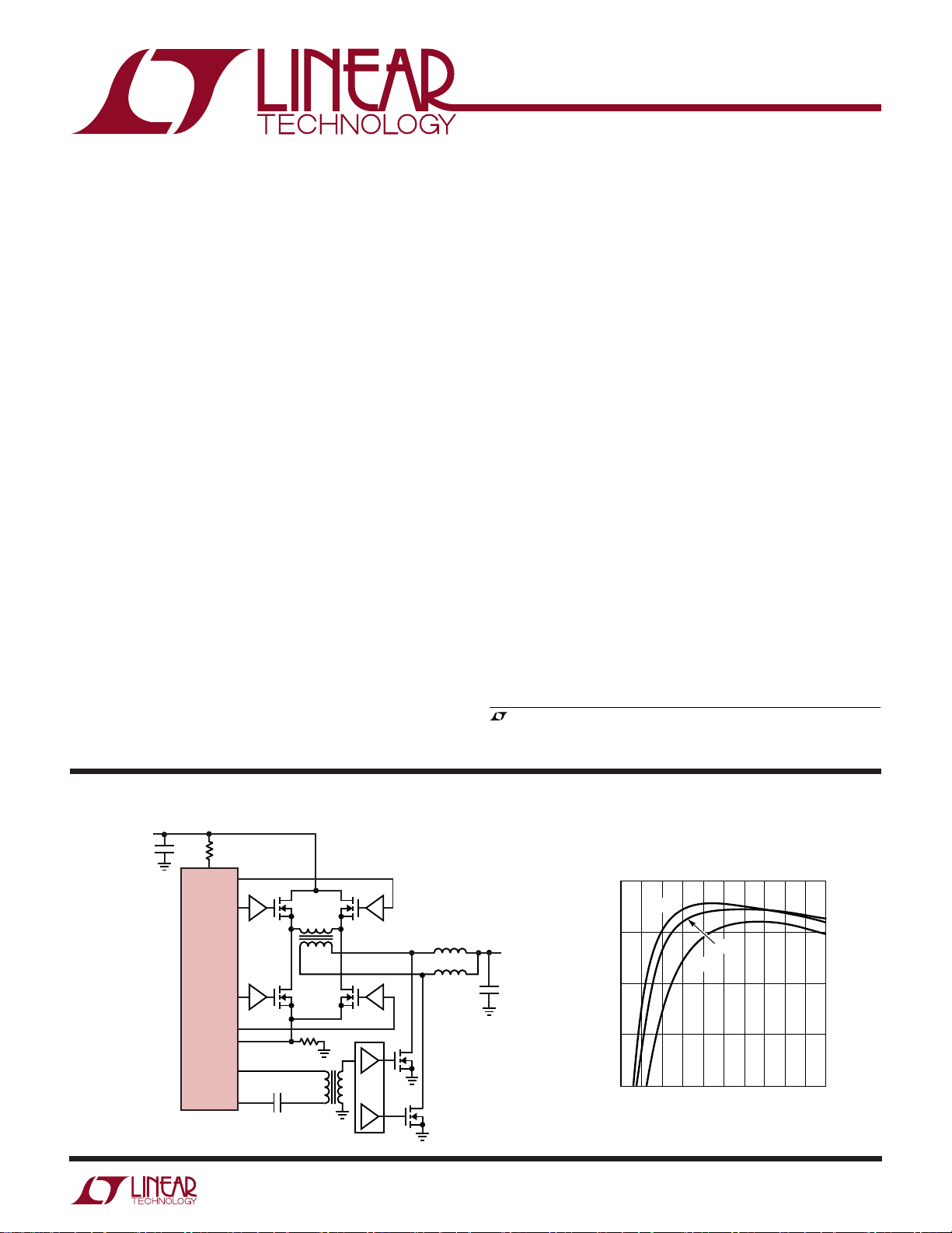
TYPICAL APPLICATIO
V
IN
36V TO 72V
C
IN
R1
U1 U2
LTC3722
U1, U2: LTC4440 GATE DRIVER
U3: LTC3901 GATE DRIVER
C1
U
MA
T1
MBMCMD
RCS
12V
, 240W Converter Efficiency
OUT
95
36V
IN
L1
L2
ME
T2
U3
MF
3722 • TA01A
V
OUT
12V
C
OUT
90
85
EFFICIENCY (%)
80
75
0
48V
IN
72V
IN
42 6 10 14 18
12
8
CURRENT (A)
16
3722 TA01b
20
372212f
1
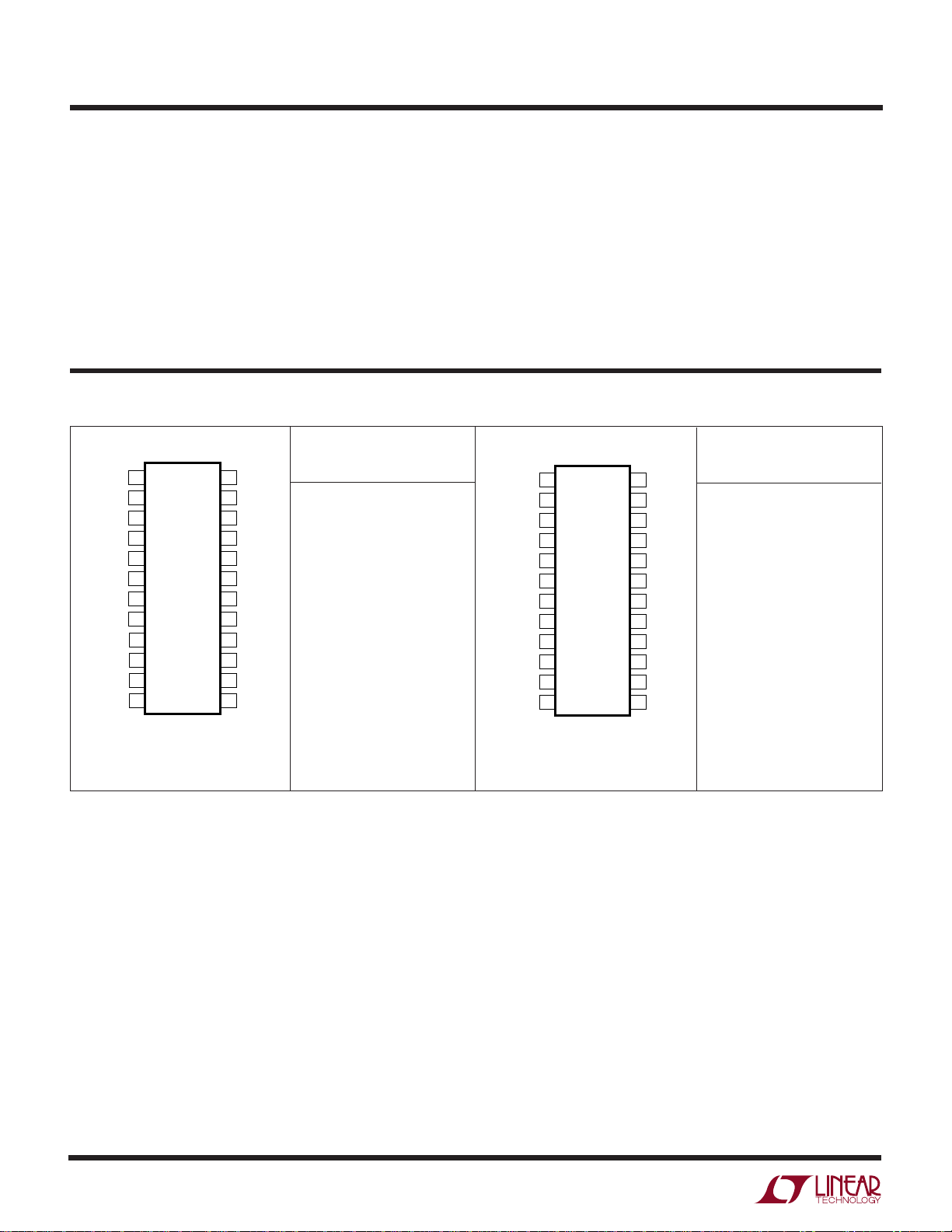
LTC3722-1/LTC3722-2
1
2
3
4
5
6
7
8
9
10
11
12
TOP VIEW
GN PACKAGE
24-LEAD NARROW PLASTIC SSOP
24
23
22
21
20
19
18
17
16
15
14
13
SYNC
RAMP
CS
COMP
DPRG
FB
SS
NC
PDLY
SBUS
ADLY
UVLO
C
T
GND
PGND
OUTA
OUTB
OUTC
V
CC
OUTD
OUTE
OUTF
V
REF
SPRG
WW
W
U
ABSOLUTE AXI U RATI GS
(Note 1)
VCC to GND (Low Impedance Source) ......... –0.3 to 10V
(Chip Self Regulates at 10.3V)
UVLO to GND................................................–0.3 to V
CC
All Other Pins to GND
(Low Impedance Source) ....................... –0.3 to 5.5V
VCC (Current Fed) ................................................. 25mA
UUW
PACKAGE/ORDER I FOR ATIO
ORDER PART
NUMBER
LTC3722EGN-1
SYNC
DPRG
COMP
RLEB
NC
PDLY
SBUS
ADLY
UVLO
TOP VIEW
1
2
3
CS
4
5
6
FB
7
SS
8
9
10
11
12
24
C
T
23
GND
22
PGND
21
OUTA
20
OUTB
19
OUTC
18
V
CC
17
OUTD
16
OUTE
15
OUTF
14
V
REF
13
SPRG
V
Output Current ................................ Self Regulated
REF
Outputs (A,B,C,D,E,F) Current .......................... ±100mA
Operating Temperature Range (Note 6)
LTC3722E........................................... –40°C to 85°C
Storage Temperature Range ................. –65°C to 150°C
Lead Temperature (Soldering, 10 sec)..................300°C
ORDER PART
NUMBER
LTC3722EGN-2
24-LEAD NARROW PLASTIC SSOP
T
JMAX
Consult LTC Marketing for parts specified with wider operating temperature ranges.
2
GN PACKAGE
= 125°C, θJA = 100°C/W
T
= 125°C, θJA = 100°C/W
JMAX
372212f
LTC3722-1/LTC3722-2
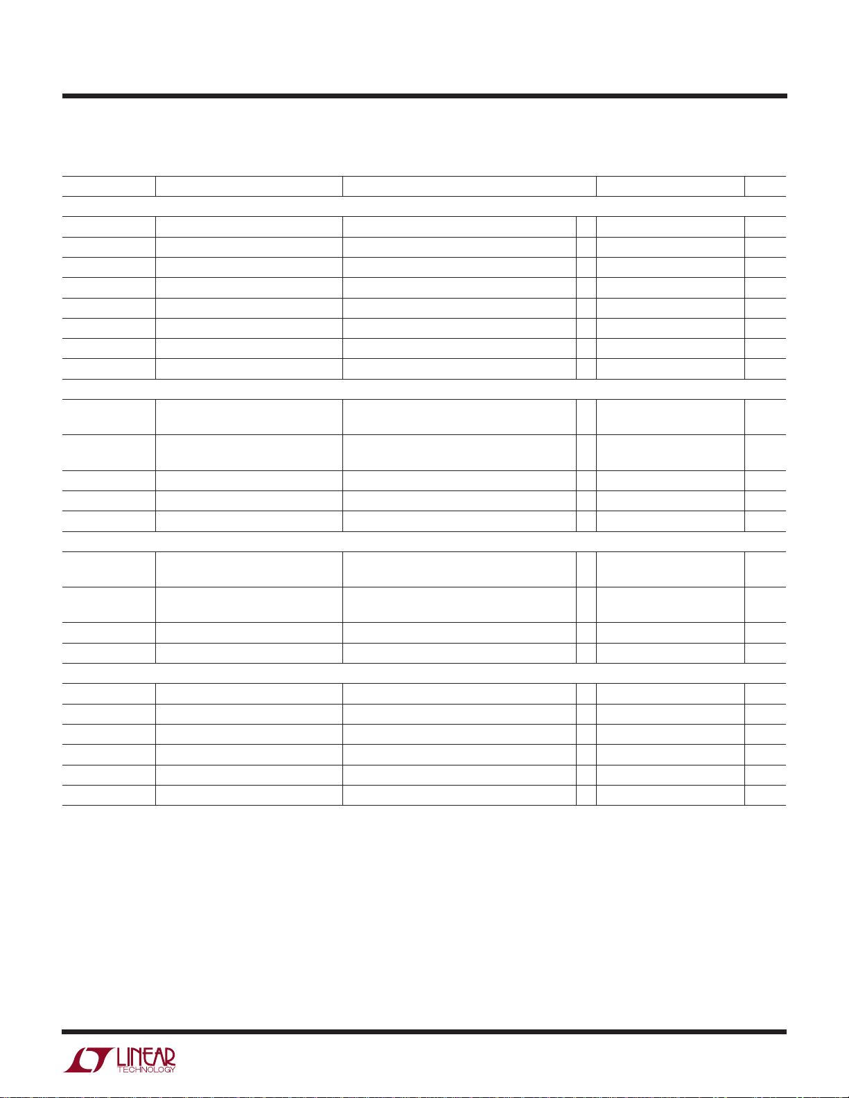
ELECTRICAL CHARACTERISTICS
temperature range, otherwise specifications are at TA = 25°C. VCC = 9.5V, CT = 270pF, R
The ● denotes the specifications which apply over the full operating
= 60.4k, R
DPRG
= 100k, unless otherwise
SPRG
noted.
SYMBOL PARAMETER CONDITIONS MIN TYP MAX UNITS
Input Supply
V
CCUV
V
CCHY
I
CCST
I
CCRN
V
SHUNT
R
SHUNT
SUVLO System UVLO Threshold Measured on UVLO Pin, 10mA into V
SHYST System UVLO Hysteresis Current Current Flows Out of UVLO Pin 8.5 10 11.5 µA
Delay Blocks
DTHR Delay Pin Threshold SBUS = 1.5V ● 1.4 1.5 1.6 V
DHYS Delay Hysteresis Current SBUS = 1.5V, ADLY/PDLY = 1.7V 1.3 mA
DTMO Delay Timeout R
DFXT Fixed Delay Threshold Measured on SBUS 4 V
DFTM Fixed Delay Time ADLY,PDLY = 1V, SBUS = V
Phase Modulator
I
RMP
I
SLP
DC
MAX
DC
MIN
Oscillator
OSCI Initial Accuracy TA = 25°C, CT = 270pF 225 250 275 kHz
OSCT Total Variation VCC = 6.5V to 9.5V ● 215 250 285 kHz
OSCV CT Ramp Amplitude Measured on C
OSYT SYNC Threshold Measured on SYNC 1.6 1.9 2.2 V
OSYW Minimum SYNC Pulse Width Measured at Outputs (Note 2) 100 ns
OSYR SYNC Frequency Range Measured at Outputs (Note 2) 1000 kHz
VCC Under Voltage Lockout Measured on V
VCC UVLO Hysteresis Measured on V
Start-Up Current VCC = V
Operating Current No Load on Outputs 5 8 mA
Shunt Regulator Voltage Current into VCC = 10mA 10.3 10.8 V
Shunt Resistance Current into VCC = 10mA to 17mA 1.1 3.5 Ω
ADLY and PDLY SBUS = 2.25V
ADLY and PDLY
DPRG
Ramp Discharge Current RAMP = 1V, COMP = 0V, CT = 4V, 50 mA
LTC3722-1 Only
Slope Compensation Current Measured on CS, CT = 1V 30 µA
Maximum Phase Shift COMP = 4.5V ● 95 98.5 %
Minimum Phase Shift COMP = 0V ● 0 0.5 %
CC
CC
– 0.3V ● 145 230 µA
UVLO
CC
= 60.4K 100 ns
REF
= 2.25V 68 µA
C
T
T
3.8 4.2 V
4.8 5.0 5.2 V
● 2.1 2.25 2.4 V
10.25 10.5 V
70 ns
2.2 V
372212f
3
LTC3722-1/LTC3722-2
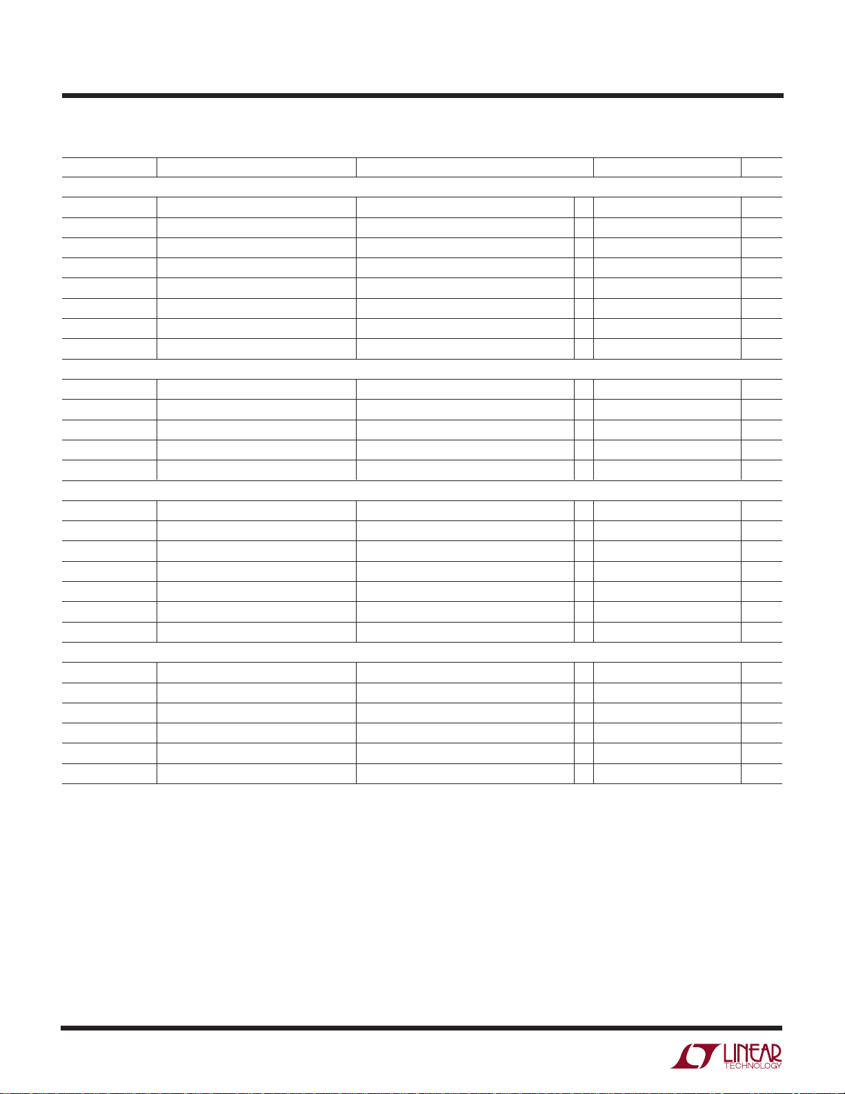
ELECTRICAL CHARACTERISTICS
The ● denotes the specifications which apply over the full operating
temperature range, otherwise specifications are at TA = 25°C. VCC = 9.5V, unless otherwise noted.
SYMBOL PARAMETER CONDITIONS MIN TYP MAX UNITS
Error Amplifier
V
FB
FBI FB Input Range Measured on FB (Note 5) –0.3 2.5 V
A
VOL
IIB Input Bias Current COMP = 2.5V (Note 4) 5 20 nA
V
OH
V
OL
I
SOURCE
I
SINK
Reference
V
REF
REFLD Load Regulation Load on V
REFLN Line Regulation VCC = 6.5V to 9.5V 0.9 10 mV
REFTV Total Variation Line, Load ● 4.900 5.000 5.100 V
REFSC Short-Circuit Current V
Outputs
OUTH(x) Output High Voltage I
OUTL(x) Output Low Voltage I
R
HI(x)
R
LO(x)
t
r(x)
t
f(x)
SDEL SYNC Driver Turn-0ff Delay R
Current Limit and Shutdown
CLPP Pulse by Pulse Current Limit Threshold Measured on CS 270 300 330 mV
CLSD Shutdown Current Limit Threshold Measured on CS 0.55 0.65 0.73 V
CLDEL Current Limit Delay to Output 100mV Overdrive on CS (Notes 3, 7) 80 ns
SSI Soft-Start Current SS = 2.5V 7 12 17 µA
SSR Soft-Start Reset Threshold Measured on SS 0.7 0.4 0.1 V
FLT Fault Reset Threshold Measured on SS 4.5 3.9 3.5 V
Note 1: Absolute Maximum Ratings are those values beyond which the life
of a device may be impaired.
Note 2: Sync amplitude = 5V
frequency = 1/2 sync frequency.
Note 3: Includes leading edge blanking delay, R
Note 4: FB is driven by a servo-loop amplifier to control V
tests.
Note 5: Set FB to –0.3V, 2.5V and insure that COMP does not phase
invert.
FB Input Voltage COMP = 2.5V (Note 4) 1.172 1.204 1.236 V
Open-Loop Gain COMP = 1V to 3V (Note 4) 70 90 dB
Output High Load on COMP = –100µA 4.7 4.92 V
Output Low Load on COMP = 100µA 0.18 0.4 V
Output Source Current COMP = 2.5V 400 800 µA
Output Sink Current COMP = 2.5V 2 5 mA
Initial Accuracy TA = 25°C, Measured on V
= 100µA to 5mA 2 15 mV
REF
Shorted to GND 18 30 45 mA
REF
= –50mA 7.9 8.4 V
OUT(x)
= 50mA 0.6 1 V
OUT(x)
Pull-Up Resistance I
Pull-Down Resistance I
Rise Time C
Fall Time C
= –50mA to –10mA 22 30 Ω
OUT(x)
= –50mA to –10mA 12 20 Ω
OUT(x)
= 50pF (Note 8) 5 15 ns
OUT(x)
= 50pF (Note 8) 5 15 ns
OUT(x)
= 100k 180 ns
SPRG
REF
4.925 5.00 5.075 V
Note 6: The LTC3722E-1/LTC3722E-2 are guaranteed to meet
performance specifications from 0°C to 85°C. Specifications over the
, pulse width = 50ns. Verify output (A-F)
P-P
= 20k.
LEB
for these
COMP
–40°C to 85°C operating temperature range are assured by design,
characterization and correlation with statistical process controls.
Note 7: Guaranteed by design, not tested in production.
Note 8: Rise time is measured from the 10% to 90% points of the rising
edge of the driver output signal. Fall time is measured from the 90% to
10% points of the falling edge of the driver output signal.
4
372212f

UW
TEMPERATURE (°C)
FREQUENCY (kHz)
240
250
80
3722 • G03
230
220
–40–60 – 20 200 40 60 100
260
CT = 270pF
TEMPERATURE (°C)
V
REF
(V)
4.99
5.00
80
3722 • G06
4.98
4.97
–40–60 – 20 200 40 60 100
5.01
TYPICAL PERFOR A CE CHARACTERISTICS
Start-Up ICC vs V
200
TA = 25°C
CC
10.50
VCC vs I
TA = 25°C
SHUNT
LTC3722-1/LTC3722-2
Oscillator Frequency vs
Temperature
150
100
(µA)
CC
I
50
0
2
0
4
VCC (V)
Leading Edge Blanking Time
vs R
LEB
350
TA = 25°C
300
250
200
150
BLANK TIME (ns)
100
50
10.25
(V)
10.00
CC
V
9.75
(V)
REF
V
9.50
5.05
5.00
4.95
4.90
4.85
0
V
REF
10
vs I
TA = 25°C
REF
20
I
SHUNT
TA = 85°C
30
(mA)
TA = –40°C
40
50
3722 • G02
V
vs Temperature
REF
6
8
10
3722 • G01
GAIN (dB)PHASE (DEG)
0
0
40
2010 30 50 70 90
R
LEB
60 80
(kΩ)
Error Amplifier Gain/Phase
TA = 25°C
100
80
60
40
20
0
–180
–270
–360
10 1k100 10k 100k 10M
FREQUENCY (Hz)
3722 • G04
1M
100
3722 • G07
4.80
0
510
15 25 40
I
REF
Start-Up ICC vs Temperature
190
180
170
160
150
(µA)
140
CC
I
130
120
110
100
–25 5 35 95 12565
–55
TEMPERATURE (°C)
20
(mA)
30 35
3722 • G05
3722 • G08
Delay Hysteresis Current vs
Temperature
1.302
SBUS = 1.5V
1.300
1.298
1.296
1.294
1.292
1.290
1.288
1.286
HYSTERESIS CURRENT (mA)
1.284
1.282
1.280
–25 5 35 95 12565
–55
TEMPERATURE (°C)
3722 • G09
372212f
5
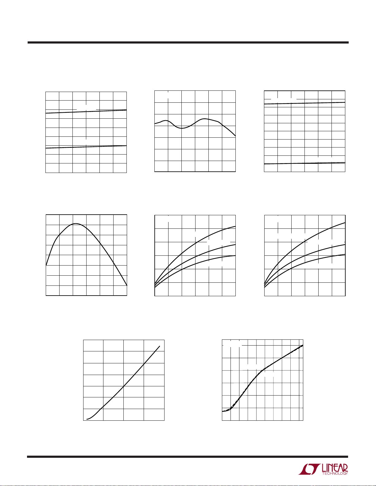
LTC3722-1/LTC3722-2
UW
TYPICAL PERFOR A CE CHARACTERISTICS
Slope Current vs Temperature
90
80
70
60
50
40
CURRENT (µA)
30
20
10
0
–25 5 35 95 12565
–55
CT = 2.25V
CT = 1V
TEMPERATURE (°C)
FB Input Voltage vs Temperature
1.205
1.204
1.203
1.202
1.201
1.200
FB VOLTAGE (V)
1.199
1.198
1.197
–25 5 35 95 12565
–55
TEMPERATURE (°C)
3722 • G10
3722 • G13
VCC Shunt Voltage vs
Temperature
10.5
ICC = 10mA
10.4
10.3
10.2
10.1
SHUNT VOLTAGE (V)
10.0
9.9
9.8
–25 5 35 95 12565
–55
Delay Timeout vs R
300
TA = 25°C
250
200
150
DELAY (ns)
100
50
0
10
60
TEMPERATURE (°C)
DPRG
SBUS = 2.25V
110 160 210
R
(kΩ)
DPRG
3722 • G11
SBUS = 1.5V
SBUS = 1.125V
260 310
3722 • G14
Delay Pin Threshold vs
Temperature
2.4
2.3
SBUS = 2.25V
2.2
2.1
2.0
1.9
1.8
THRESHOLD (V)
1.7
1.6
1.5
1.4
–25 5 35 95 12565
–55
TEMPERATURE (°C)
ZVS Delay in Fixed Mode,
SBUS = 5V
300
TA = 25°C
250
ADLY = PDLY = 2.25V
200
150
DELAY (ns)
100
50
0
10
110 160 210
60
SBUS = 1.5V
ADLY = PDLY = 1.5V
ADLY = PDLY = 1.125V
R
(kΩ)
DPRG
3722 • G12
260 310
3722 • G15
6
Synchronous Driver Turn-Off
Delay in Fixed Mode
350
TA = 25°C
300
250
200
150
DELAY (nS)
100
50
0
10
60 110 210
R
(kΩ)
SPRG
160
3722 • G16
Synchronous Driver Turn-Off Delay
in Adaptive Mode, SBUS = 1.5V
TA = 25°C
260
220
30
B HI-F LOW
70
50
R
90
SPRG
A HI-E LOW
130 170
110
(kΩ)
150
180
140
DELAY (ns)
100
60
20
10
190
3722 • G17
372212f

LTC3722-1/LTC3722-2
U
PI FU CTIO S
SYNC (Pin 1/Pin 1): Synchronization Input/Output for the
Oscillator. The input threshold for SYNC is approximately
1.9V, making it compatible with both CMOS and TTL logic.
Terminate SYNC with a 5.1k resistor to GND.
DPRG (Pin 2/Pin 5): Programming Input for Default Zero
Voltage Transition (ZVS) Delay. Connect a resistor from
DPRG to V
outputs A, B, C, D. The nominal voltage on DPRG is 2V.
RAMP (NA/Pin 2): Input to Phase Modulator Comparator
for LTC3722-2 only. The voltage on RAMP is internally
level shifted by 650mV.
CS (Pin 3/Pin 3): Input to phase modulator for the
LTC3722-1. Input to Pulse by Pulse and Overload Current
Limit Comparators, Output of Slope Compensation Circuitry. The pulse by pulse comparator has a nominal
300mV threshold, while the overload comparator has a
nominal 650mV threshold.
COMP (Pin 4/Pin 4): Error Amplifier Output, Inverting
Input to Phase Modulator.
REF
UU
(LTC3722-1/LTC3722-2)
to set the maximum turn on delay for
SBUS (Pin 10/Pin 10): Line Voltage Sense Input. SBUS is
connected to the main DC voltage feed by a resistive
voltage divider when using adaptive ZVS control. The
voltage divider is designed to produce 1.5V on SBUS at
nominal VIN. If SBUS is tied to V
LTC3722-2 is configured for fixed mode ZVS control.
ADLY (Pin 11/Pin 11): Active Leg Delay Circuit Input.
ADLY is connected through a voltage divider to the right
leg of the bridge in adaptive ZVS mode. In fixed ZVS mode,
a voltage between 0V and 2.5V on ADLY, programs a fixed
ZVS delay time for the active leg transition.
UVLO (Pin 12/Pin 12): Input to Program System Turn-On
and Turn-Off Voltages. The nominal threshold of the UVLO
comparator is 5V. UVLO is connected to the main DC
system feed through a resistor divider. When the UVLO
threshold is exceeded, the LTC3722-1/LTC3722-2 commences a soft start cycle and a 10µA (nominal) current is
fed out of UVLO to program the desired amount of system
hysteresis. The hysteresis level can be adjusted by changing the resistance of the divider.
, the LTC3722-1/
REF
R
(Pin 5/NA): Timing Resistor for Leading Edge Blank-
LEB
ing. Use a 10k to 100k resistor to program from 40ns to
310ns of leading edge blanking of the current sense signal
on CS for the LTC3722-1. A ±1% tolerance resistor is
recommended. The LTC3722-2 has a fixed blanking time
of approximately 80ns.
FB (Pin 6/Pin 6): Error Amplifier Inverting Input. This is the
voltage feedback input for the LTC3722. The nominal
regulation voltage at FB is 1.204V.
SS (Pin 7/Pin 7): Soft-Start/Restart Delay Circuitry Timing
Capacitor. A capacitor from SS to GND provides a controlled ramp of the current command (LTC3722-1), or
duty cycle (LTC3722-2). During overload conditions SS is
discharged to ground initiating a soft-start cycle.
NC (Pin 8/Pin 8): No Connection. Tie this pin to GND.
PDLY (Pin 9/Pin 9): Passive Leg Delay Circuit Input. PDLY
is connected through a voltage divider to the left leg of the
bridge in adaptive ZVS mode. In fixed ZVS mode, a voltage
between 0V and 2.5V on PDLY, programs a fixed ZVS
delay time for the passive leg transition.
SPRG (Pin 13/Pin 13): A Resistor is connected between
SPRG and GND to set the turn-off delay for the synchronous rectifier driver outputs (OUTE and OUTF). The nominal voltage on SPRG is 2V.
V
(Pin 14/Pin 14): Output of the 5V Reference. V
REF
capable of supplying up to 18mA to external circuitry. V
should be decoupled to GND with a 1µF ceramic capacitor.
OUTF (Pin 15/Pin 15): 50mA Driver for Synchronous
Rectifier Associated with OUTB and OUTC.
OUTE (Pin 16/Pin 16): 50mA Driver for Synchronous
Rectifier Associated with OUTA and OUTD.
OUTD (Pin 17/Pin 17): 50mA driver for Low Side of the Full
Bridge Active Leg.
VCC (Pin 18/Pin 18): Supply Voltage Input to the
LTC3722-1/LTC3722-2 and 10.25V Shunt Regulator. The
chip is enabled after VCC has risen high enough to allow the
VCC shunt regulator to conduct current and the UVLO
comparator threshold is exceeded. Once the VCC shunt
regulator has turned on, VCC can drop to as low as 6V (typ)
and maintain operation.
REF
is
REF
372212f
7
LTC3722-1/LTC3722-2
U
PI FU CTIO S
UU
(LTC3722-1/LTC3722-2)
OUTC (Pin 19/Pin 19): 50mA Driver for High Side of the
Full Bridge Active Leg.
OUTB (Pin 20/Pin 20): 50mA Driver for Low Side of the
Full Bridge Passive Leg.
OUTA (Pin 21/Pin 21): 50mA Driver for High Side of the
Full Bridge Passive Leg.
PGND (Pin 22/Pin 22): Power Ground for the LTC3722.
The output drivers of the LTC3722 are referenced to
W
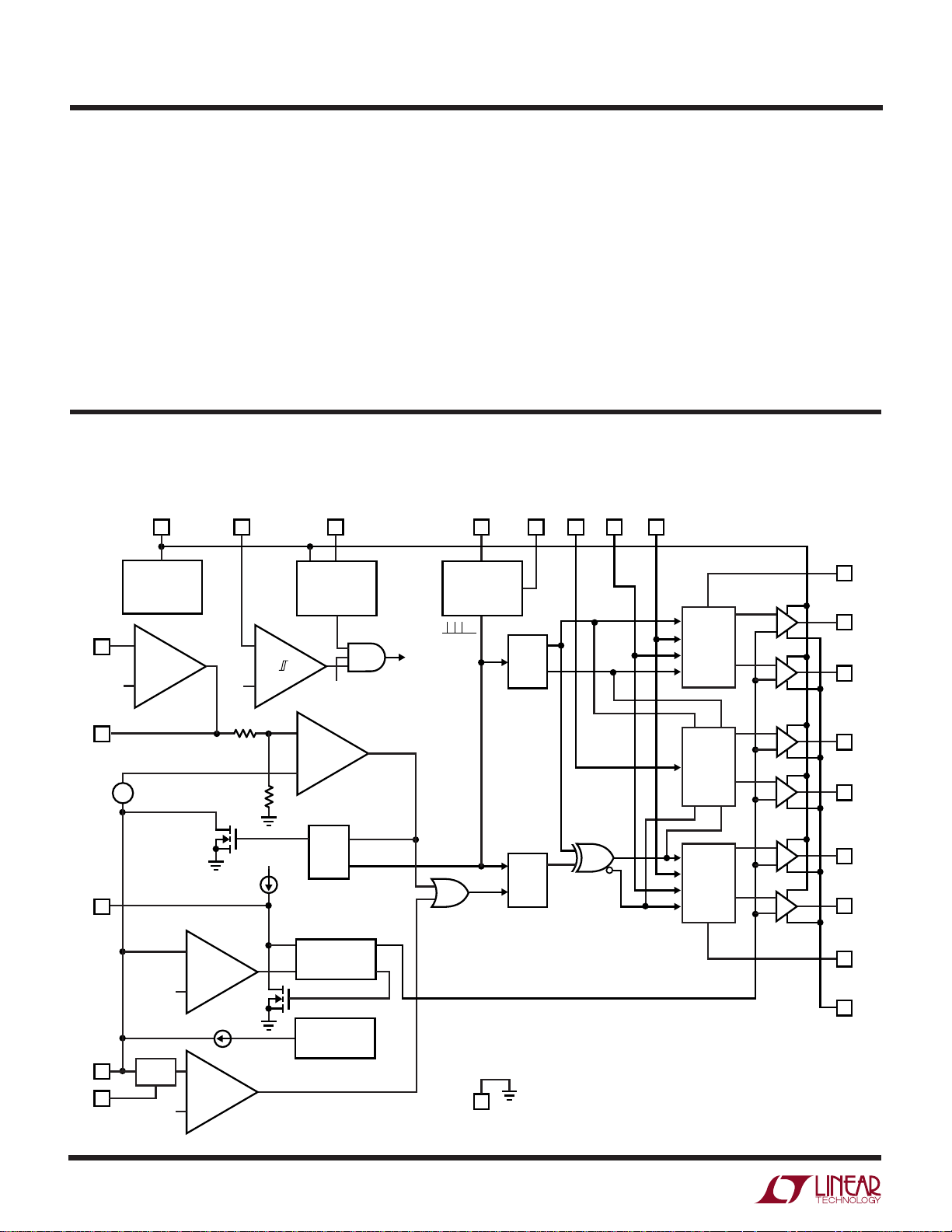
BLOCK DIAGRA S
LTC3722-1 Current Mode SYNC Phase Shift PWM
FB
6
1.2V
COMP
4
+
–
V
CC
18 12 14
V
UVLO
CC
10.25V = ON
6V = OFF
–
+
ERROR
AMPLIFIER
650mV
UVLO V
REF AND LDO
REF GOOD
SYSTEM
+
UVLO
–
5V
R1
50k
–
+
R2
14.9k
REF
5V
1.2V
V
CC
GOOD
PHASE
MODULATOR
1 = ENABLE
0 = DISABLE
PGND. Connect the ceramic VCC bypass capacitor directly
to PGND.
GND (Pin 23/Pin 23): All circuits other than the output
drivers in the LTC3722 are referenced to GND. Use of a
ground plane is recommended but not absolutely
necessary.
CT (Pin 24/Pin 24): Timing Capacitor for the Oscillator.
Use a ±5% or better low ESR ceramic capacitor for best
results.
C
24
OSC
SYNC SPRG SBUSDPRG
T
T
QB
1 13 102
Q
PASSIVE
DELAY
SYNC
RECTIFIER
DRIVE
LOGIC
PDLY
9
OUTA
21
OUTB
20
OUTE
16
OUTF
15
8
M1
V
REF
SHUTDOWN
+
–
+
–
12µA
CURRENT
LIMIT
M2
PULSE BY PULSE
CURRENT LIMIT
SS
7
650mV
CS
3
BLANK
5
LEB
300mV
R
QB
R
S
Q
FAULT
LOGIC
SLOPE
COMPENSATION
/R
C
T
23
GND
OUTC
R
QB
S
ACTIVE
DELAY
19
OUTD
17
ADLY
11
PGND
22
3722 • BD01
372212f
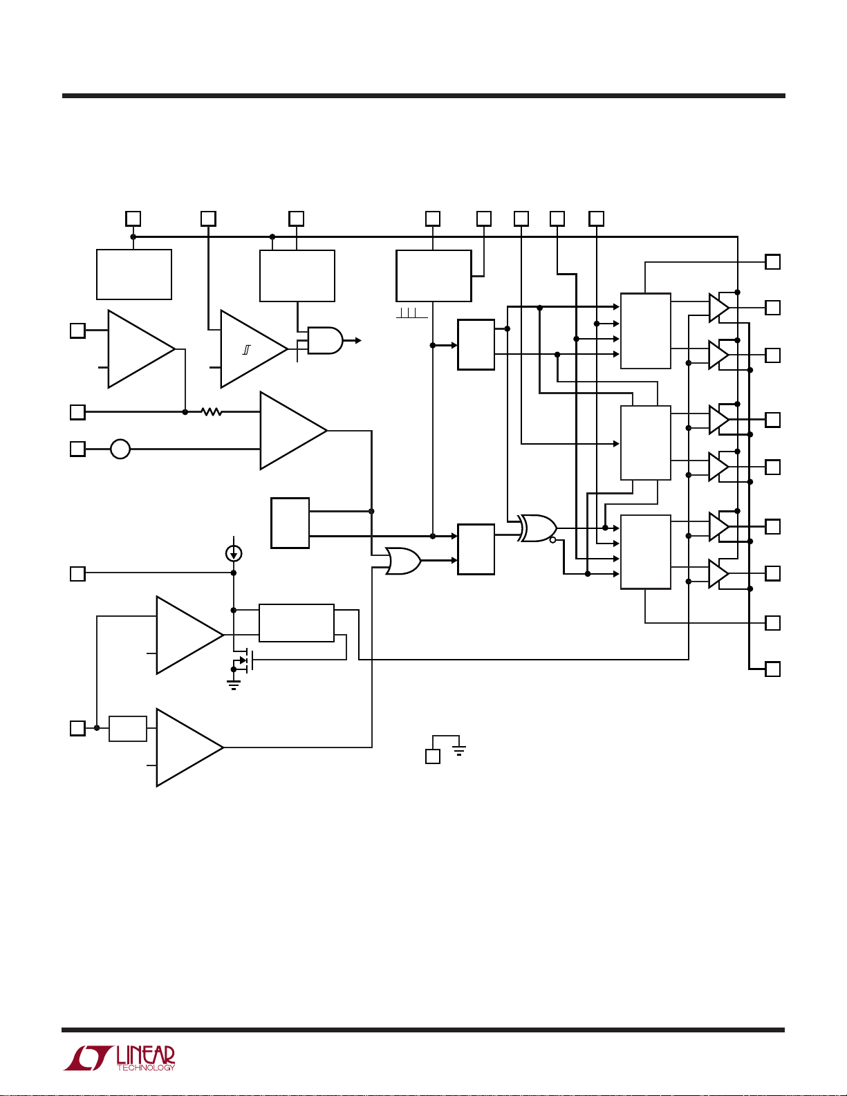
W
BLOCK DIAGRA S
LTC3722-1/LTC3722-2
LTC3722-2 Voltage Mode SYNC Phase Shift PWM
FB
6
1.2V
COMP
4
2
RAMP
SS
7
V
CC
18 12 14
V
UVLO
CC
10.25V = ON
6V = OFF
–
AMPLIFIER
+
+
–
650mV
UVLO V
ERROR
5V
R1
50k
12µA
SHUTDOWN
CURRENT
LIMIT
+
–
V
REF
+
REF AND LDO
REF GOOD
SYSTEM
UVLO
–
+
MODULATOR
QB
Q
REF
5V
1.2V
V
CC
GOOD
PHASE
FAULT
LOGIC
C
24
OSC
1 = ENABLE
0 = DISABLE
R
S
SYNC SPRG SBUSDPRG
T
T
QB
R
S
1 13 105
Q
QB
PASSIVE
DELAY
SYNC
RECTIFIER
DRIVE
LOGIC
ACTIVE
DELAY
PDLY
9
OUTA
21
OUTB
20
OUTE
16
OUTF
15
OUTC
19
OUTD
17
ADLY
11
650mV
CS
3
BLANK
300mV
–
+
–
M2
PULSE BY PULSE
CURRENT LIMIT
3722 • BD02
23
GND
PGND
22
372212f
9
 Loading...