

FEATURES
LTC3719
2-Phase, High Efficiency,
Step-Down Controller for
AMD Opteron™ CPUs
U
DESCRIPTIO
■
Output Stages Operate Antiphase Reducing Input
and Output Capacitance Requirements and Power
Supply Induced Noise
■
Dual Input Supply Capability for Load Sharing
■
5-Bit AMD CPU VID Code:
V
= 0.8V to 1.55V
■
■
■
■
■
■
■
■
■
■
■
■
■
OUT
±1% Output Voltage Accuracy
True Remote Sensing Differential Amplifier
Power Good Output Voltage Monitor
Supports Active Voltage Positioning
Current Mode Control Ensures Current Sharing
OPTI-LOOP® Compensation Minimizes C
OUT
Three Operational Modes: PWM, Burst and Cycle Skip
Programmable Fixed Frequency: 150kHz to 300kHz
Wide VIN Range: 4V to 36V Operation
Adjustable Soft-Start Current Ramping
Internal Current Foldback and Short-Circuit Shutdown
Overvoltage Soft Latch Eliminates Nuisance Trips
Available in 36-Lead Narrow (0.209) SSOP Package
U
APPLICATIO S
■
Servers and Workstations
, LTC and LT are registered trademarks of Linear Technology Corporation.
OPTI-LOOP and Burst Mode are registered trademarks of Linear Technology Corporation.
AMD Opteron is a trademark of Advanced Micro Devices, Inc.
The LTC®3719 is a 2-phase, VID programmable, synchronous step-down switching regulator controller that drives
two N-channel external power MOSFET stages in a fixed frequency architecture. The 2-phase controller drives its two
output stages out of phase at frequencies up to 300kHz to
minimize the RMS ripple currents in both input and output
capacitors. The 2-phase technique effectively multiplies the
fundamental frequency by two, improving transient response while operating each channel at an optimum frequency for efficiency. Thermal design is also simplified.
An operating mode select pin (FCB) can be used to select
among three modes including Burst Mode® operation for
highest efficiency. An internal differential amplifier provides
true remote sensing of the regulated supply’s positive and
negative output terminals as required in high current applications.
The RUN/SS pin provides soft-start and optional timed,
short-circuit shutdown. Current foldback limits MOSFET
dissipation during short-circuit conditions when the
overcurrent latchoff is disabled. OPTI-LOOP compensation
allows the transient response to be optimized for a wide
range of output capacitors and ESR values.
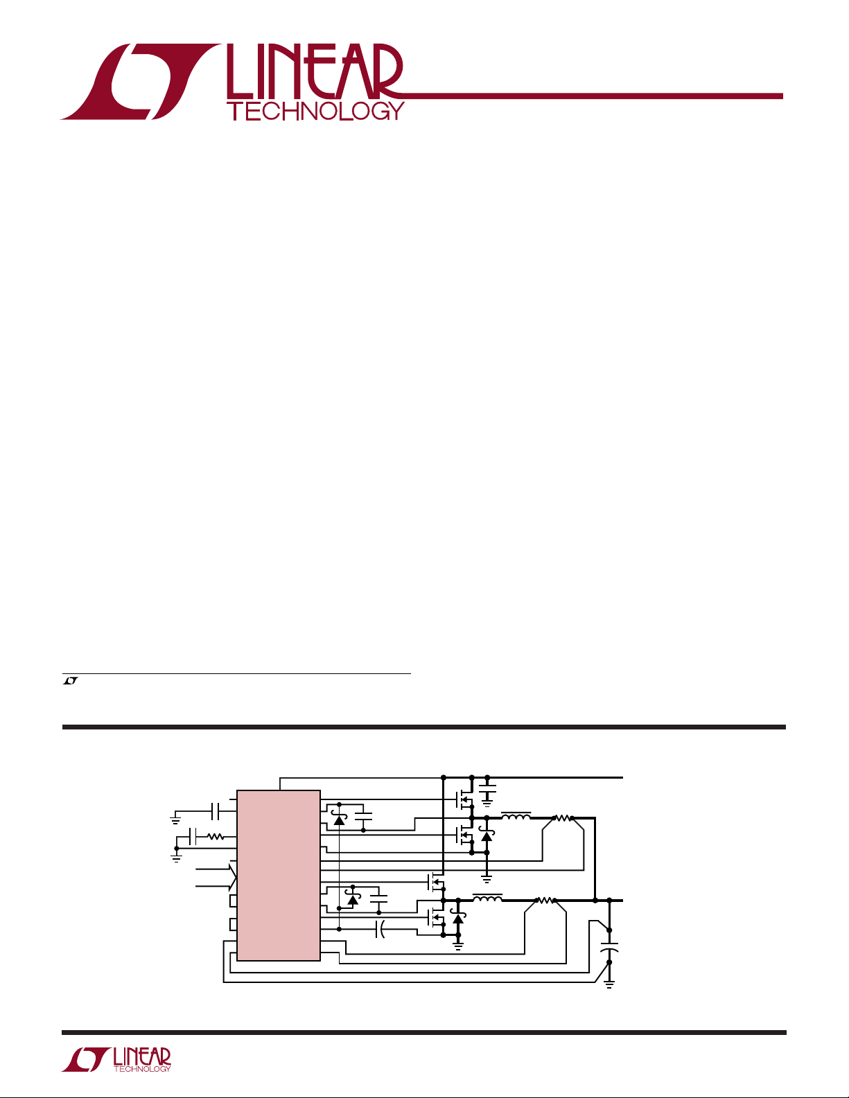
TYPICAL APPLICATIO
0.1µF
FCB
3.3k
RUN/SS
I
TH
SGND
PGOOD
VID0–VID4
EAIN
ATTENOUT
ATTENIN
V
DIFFOUT
–
V
OS
+
V
OS
220pF
5 VID BITS
U
10µF
V
IN
TG1
SW1
BG1
PGND
TG2
SW2
BG2
S
0.47µF
S
+
–
0.47µF
CC
+
–
+
10µF
LTC3719
BOOST1
SENSE1
SENSE1
BOOST2
INTV
SENSE2
SENSE2
Figure 1. High Current Dual Phase Step-Down Converter
35V
×6
D1
1µH
D2
0.002Ω
1µH
0.002Ω
+
V
IN
5V TO 28V
V
DD_CORE
0.8V TO 1.55V
45A
C
OUT
270µF
2V
×4
3716 F01
sn3719 3719fs
1
LTC3719
WW
W
U
ABSOLUTE AXI U RATI GS
(Note 1)
Input Supply Voltage (VIN).........................36V to –0.3V
Topside Driver Voltages (BOOST1,2).........42V to –0.3V
Switch Voltage (SW1, 2) .............................36V to –5 V
SENSE1+, SENSE2+, SENSE1–,
SENSE2– Voltages ...................(1.1)INTVCC to –0.3V
EAIN, V
V
VID0–VID4, Voltages ...............................7V to –0.3V
Boosted Driver Voltage (BOOST-SW) ..........7V to –0.3V
PLLFLTR, PLLIN, V
FCB Voltages ................................... INTVCC to –0.3V
ITH Voltage................................................2.7V to –0.3V
Peak Output Current <1µs(TG1, 2, BG1, 2)................ 3A
INTVCC RMS Output Current................................ 50mA
Operating Ambient Temperature Range
(Note 2) .............................................. –40°C to 85°C
Junction Temperature (Note 3)............................. 125°C
Storage Temperature Range ................. –65°C to 150°C
Lead Temperature (Soldering, 10 sec)..................300°C
+
–
, V
OS
, ATTENIN, ATTENOUT, PGOOD, NO_CPU,
BIAS
, EXTVCC, INTVCC, RUN/SS,
OS
DIFFOUT
,
UUW
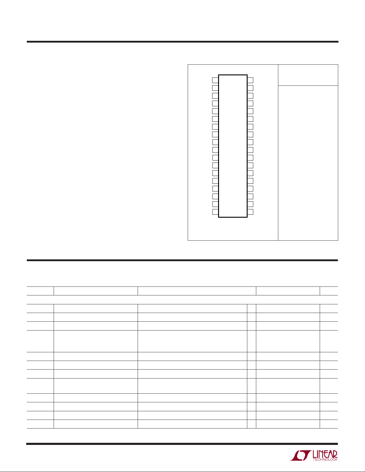
PACKAGE/ORDER I FOR ATIO
RUN/SS
SENSE1
SENSE1
EAIN
PLLFLTR
PLLIN
FCB
I
SGND
V
DIFFOUT
V
OS
V
OS
SENSE2
SENSE2
ATTENOUT
NO_CPU
VID0
VID1
TOP VIEW
1
+
2
–
3
4
5
6
7
8
TH
9
10
–
11
+
12
–
13
+
14
15
16
17
18
G PACKAGE
36-LEAD PLASTIC SSOP
T
= 125°C, θJA = 85°C/W
JMAX
36
35
34
33
32
31
30
29
28
27
26
25
24
23
22
21
20
19
PGOOD
TG1
SW1
BOOST1
V
IN
BG1
EXTV
CC
INTV
CC
PGND
BG2
BOOST2
SW2
TG2
ATTENIN
V
BIAS
VID4
VID3
VID2
ORDER PART
NUMBER
LTC3719EG
Consult LTC Marketing for parts specified with wider operating temperature ranges.
ELECTRICAL CHARACTERISTICS
temperature range, otherwise specifications are at TA = 25°C. VIN = 15V, V
The ● denotes the specifications which apply over the full operating
BIAS
= 5V, V
= 5V unless otherwise noted.
RUN/SS
SYMBOL PARAMETER CONDITIONS MIN TYP MAX UNITS
Main Control Loop
V
EAIN
V
SENSEMAX
I
INEAIN
V
LOADREG
V
REFLNREG
V
FCB
I
FCB
V
BINHIBIT
Regulated Feedback Voltage ITH Voltage = 1.2V; Measured at V
(Note 4) ● 0.594 0.600 0.606 V
EAIN
Maximum Current Sense Threshold ● 62 75 88 mV
Feedback Current (Note 4) –5 –50 nA
Output Voltage Load Regulation (Note 4)
Measured in Servo Loop, ∆I
Measured in Servo Loop, ∆I
Voltage: 1.2V to 0.7V ● 0.1 0.5 %
TH
Voltage: 1.2V to 2V ● –0.1 –0.5 %
TH
Reference Voltage Line Regulation VIN = 3.6V to 30V (Note 4) 0.002 0.02 %/V
Forced Continuous Threshold ● 0.57 0.6 0.63 V
Forced Continuous Current – 0.17 –1 µA
Burst Inhibit (Constant Frequency) Measured at FCB pin 4.3 4.8 V
Threshold
V
OVL
Output Overvoltage Threshold Measured at V
EAIN
● 0.64 0.66 0.68 V
UVLO Undervoltage Lockout VIN Ramping Down 3 3.33 4 V
g
g
m
mOL
Transconductance Amplifier g
m
ITH = 1.2V, Sink/Source 5µA (Note 4) 3 mmho
Transconductance Amplifier Gain ITH = 1.2V, (gm • ZL; No Ext Load) (Note 4) 1.5 V/mV
2
sn3719 3719fs
LTC3719
ELECTRICAL CHARACTERISTICS
temperature range, otherwise specifications are at TA = 25°C. VIN = 15V, V
The ● denotes the specifications which apply over the full operating
BIAS
= 5V, V
= 5V unless otherwise noted.
RUN/SS
SYMBOL PARAMETER CONDITIONS MIN TYP MAX UNITS
I
Q
Input DC Supply Current (Note 5)
Normal Mode 1.2 mA
I
RUN/SS
V
RUN/SS
V
RUN/SSLO
I
SCL
I
SDLHO
I
SENSE
DF
MAX
Shutdown V
Soft-Start Charge Current V
RUN/SS Pin ON Threshold V
RUN/SS Pin Latchoff Arming V
RUN/SS Discharge Current Soft Short Condition V
Shutdown Latch Disable Current V
Total Sense Pins Source Current Each Channel: V
Maximum Duty Factor In Dropout 98 99.5 %
= 0V 20 40 µA
RUN/SS
= 1.9V –0.5 –1.2 µA
RUN/SS
Rising 1.0 1.5 1.9 V
RUN/SS
Rising from 3V 4.1 4.5 V
RUN/SS
= 0.5V, V
EAIN
= 0.5V 1.6 5 µA
EAIN
SENSE1–, 2
– = V
SENSE1+, 2
= 4.5V 0.5 2 4 µA
RUN/SS
+ = 0V –85 –60 µA
Top Gate Transition Time: (Note 6)
TG1, 2 t
TG1, 2 t
Rise Time C
r
Fall Time C
f
= 3300pF 30 90 ns
LOAD
= 3300pF 40 90 ns
LOAD
Bottom Gate Transition Time: (Note 6)
BG1, 2 t
BG1, 2 t
TG/BG t
Rise Time C
r
Fall Time C
f
Top Gate Off to Bottom Gate On Delay C
1D
= 3300pF 30 90 ns
LOAD
= 3300pF 20 90 ns
LOAD
= 3300pF Each Driver (Note 6) 90 ns
LOAD
Synchronous Switch-On Delay Time
BG/TG t
Bottom Gate Off to Top Gate On Delay C
2D
= 3300pF Each Driver (Note 6) 90 ns
LOAD
Top Switch-On Delay Time
t
ON(MIN)
Minimum On-Time Tested with a Square Wave (Note 7) 180 ns
Internal VCC Regulator
V
INTVCC
V
LDO
V
LDO
V
EXTVCC
V
LDOHYS
Internal VCC Voltage 6V < VIN < 30V, V
INT INTVCC Load Regulation ICC = 0 to 20mA, V
EXT EXTVCC Voltage Drop ICC = 20mA, V
EXTVCC
EXTVCC Switchover Voltage ICC = 20mA, EXTV
EXTVCC Switchover Hysteresis ICC = 20mA, EXTV
= 4V 4.8 5.0 5.2 V
EXTVCC
= 4V 0.2 1.0 %
EXTVCC
= 5V 80 160 mV
Ramping Positive ● 4.5 4.7 V
CC
Ramping Negative 0.2 V
CC
VID Parameters
V
BIAS
R
ATTEN
Operating Supply Voltage Range 2.7 5.5 V
Resistance Between ATTENIN 10 kΩ
and ATTENOUT Pins
ATTEN
R
PULLUP
VID
THLOW
VID
THHIGH
VID
LEAK
V
NO_CPU
Resistive Divider Error ● – 0.35 0.25 %
ERR
VID0 to VID4 Pull-Up Resistance (Note 8) 40 kΩ
VID0 to VID4 Logic Threshold Low 0.4 V
VID0 to VID4 Logic Threshold High 1.6 V
VID0 to VID4 Leakage V
NO_CPU Maximum Output Voltage I
< VID0–VID4 < 7V ±1 µA
BIAS
= 2mA 0.4 V
NO_CPU
sn3719 3719fs
3
LTC3719
ELECTRICAL CHARACTERISTICS
temperature range, otherwise specifications are at TA = 25°C. VIN = 15V, V
The ● denotes the specifications which apply over the full operating
BIAS
= 5V, V
= 5V unless otherwise noted.
RUN/SS
SYMBOL PARAMETER CONDITIONS MIN TYP MAX UNITS
Oscillator and Phase-Locked Loop
f
NOM
f
LOW
f
HIGH
R
PLLIN
I
PLLFLTR
R
RELPHS
Nominal Frequency V
Lowest Frequency V
Highest Frequency V
= 1.2V 190 220 250 kHz
PLLFLTR
= 0V 120 140 160 kHz
PLLFLTR
≥ 2.4V 280 310 360 kHz
PLLFLTR
PLLIN Input Resistance 50 kΩ
Phase Detector Output Current
Sinking Capability f
Sourcing Capability f
PLLIN
PLLIN
< f
> f
OSC
OSC
–15 µA
15 µA
Controller 2-Controller 1 Phase 180 Deg
PGOOD Output
V
PGL
I
PGOOD
V
PG
PGOOD Voltage Low I
PGOOD Leakage Current V
PGOOD Trip Level, Either Controller V
= 2mA 0.1 0.3 V
PGOOD
= 5V ±1 µA
PGOOD
with Respect to Set Output Voltage
EAIN
Ramping Negative –8 – 10 – 12 %
V
EAIN
Ramping Positive 8 10 12 %
V
EAIN
Differential Amplifier/Op Amp Gain Block
A
DA
CMRR
R
IN
Differential Amplifier Gain V
Common Mode Rejection Ratio 0V < VCM < 5V; V
DA
= 0V 0.995 1 1.005 V/V
AMPMD
Input Resistance Measured at VOS+ Input; V
= 0V 46 55 dB
AMPMD
= 0V 80 kΩ
AMPMD
Note 1: Absolute Maximum Ratings are those values beyond which the
life of a device may be impaired.
Note 2: The LTC3719EG is guaranteed to meet performance specifications
from 0°C to 70°C. Specifications over the –40°C to 85°C operating
temperature range are assured by design, characterization and correlation
with statistical process controls.
Note 3: T
dissipation P
is calculated from the ambient temperature TA and power
J
according to the following formula:
D
LTC3719EG: TJ = TA + (PD • 85°C/W)
Note 4: The LTC3719 is tested in a feedback loop that servos V
specified voltage and measures the resultant V
EAIN
.
ITH
to a
Note 5: Dynamic supply current is higher due to the gate charge being
delivered at the switching frequency. See Applications Information.
Note 6: Rise and fall times are measured using 10% and 90% levels. Delay
times are measured using 50% levels.
Note 7: The minimum on-time condition corresponds to the on inductor
peak-to-peak ripple current ≥40% I
(see Minimum On-Time
MAX
Considerations in the Applications Information section).
Note 8: Each built-in pull-up resistor attached to the VID inputs also has a
series diode to allow input voltages higher than the VIDV
supply without
CC
damage or clamping (see the Applications Information section).
4
sn3719 3719fs
UW
TEMPERATURE (
°C)
–50
INTV
CC
AND EXTV
CC
SWITCH VOLTAGE (V)
4.95
5.00
5.05
25 75
3719 G06
4.90
4.85
–25 0
50 100 125
4.80
4.70
4.75
INTVCC VOLTAGE
EXTVCC SWITCHOVER THRESHOLD
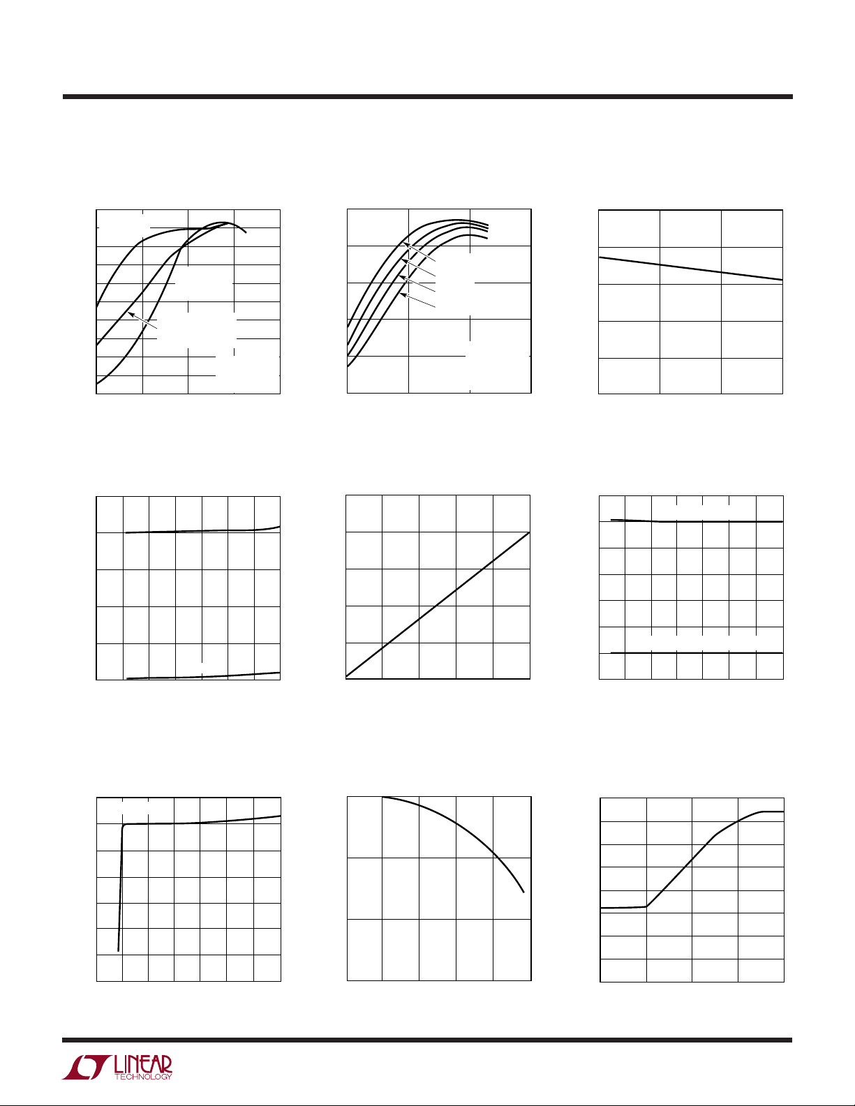
TYPICAL PERFOR A CE CHARACTERISTICS
LTC3719
Efficiency vs Load Current
(3 Operating Modes) (Figure 12)
100
Burst Mode
90
OPERATION
80
70
60
50
40
EFFICIENCY (%)
30
20
10
0
0.01
FORCED
CONTINUOUS
MODE
CONSTANT
FREQUENCY
(BURST DISABLED)
0.1
1
LOAD CURRENT (A)
V
= 5V
IN
V
= 1.55V
OUT
FREQ = 200kHz
3719 G01
10010
Efficiency vs Load Current
(Figure 12)
100
80
60
40
EFFICIENCY (%)
20
0
0.1
Supply Current vs Input Voltage
and Mode EXTVCC Voltage Drop
1000
800
600
ON
250
200
150
VIN = 5V
VIN = 8V
VIN = 12V
VIN = 20V
V
= 1.55V
OUT
V
= 0V
EXTVCC
FREQ = 200kHz
= 0V
V
FCB
1 10 100
LOAD CURRENT (A)
3719 G02
Efficiency vs Input Voltage
(Figure 12)
100
I
= 20A
OUT
= 1.55V
V
OUT
90
80
70
EFFICIENCY (%)
60
50
5
10
INPUT VOLTAGE (V)
INTVCC and EXTVCC Switch
Voltage vs Temperature
15
20
3719 G03
400
SUPPLY CURRENT (µA)
200
0
05
5.1
5.0
4.9
4.8
VOLTAGE (V)
4.7
CC
INTV
4.6
4.5
4.4
0
10
INPUT VOLTAGE (V)
I
= 1mA
LOAD
510
INPUT VOLTAGE (V)
SHUTDOWN
20
15
20 30 35
15 25
100
VOLTAGE DROP (mV)
CC
EXTV
50
0
10
30
35
3719 G04
25
0
CURRENT (mA)
30
40
20
50
3719 G05
Maximum Current Sense Threshold
vs Percent of Nominal Output
Voltage (Foldback)Internal 5V LDO Line Reg
80
70
60
50
(mV)
40
SENSE
V
30
20
10
0
0
25
PERCENT OF NOMINAL OUTPUT VOLTAGE (%)
50
75
3719 G09
sn3719 3719fs
100
3719 G07
Maximum Current Sense Threshold
vs Duty Factor
75
50
(mV)
SENSE
V
25
0
0
20 40 60 80
DUTY FACTOR (%)
100
3719 G08
5
LTC3719
UW
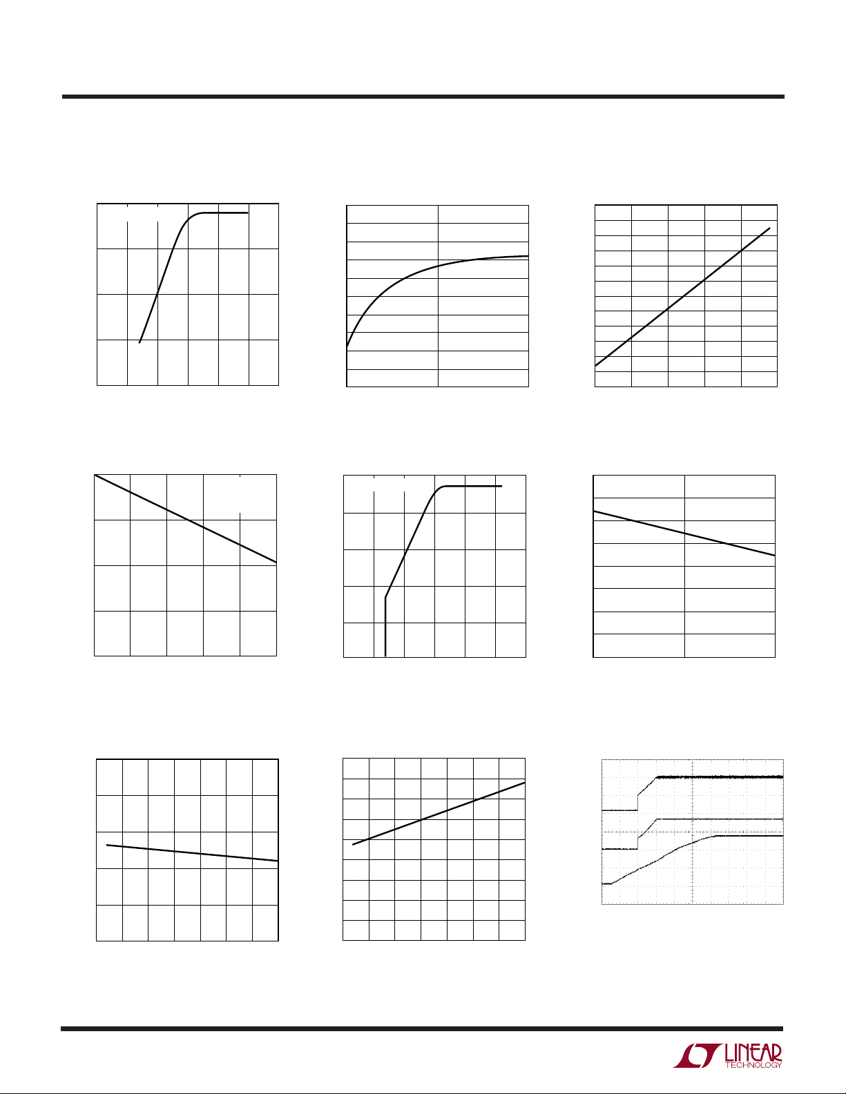
TYPICAL PERFOR A CE CHARACTERISTICS
Maximum Current Sense Threshold
(mV)
SENSE
V
20
80
60
40
0
vs V
V
SENSE(CM)
0
(Soft-Start)
RUN/SS
= 1.55V
1234
V
(V)
RUN/SS
56
3719 G10
Load Regulation V
0.0
–0.1
(%)
OUT
–0.2
NORMALIZED V
–0.3
FCB = 0V
= 15V
V
IN
FIGURE 1
Maximum Current Sense Threshold
vs Sense Common Mode Voltage
80
76
72
(mV)
SENSE
68
V
64
60
(V)
ITH
V
2.5
2.0
1.5
1.0
0.5
0
COMMON MODE VOLTAGE (V)
vs V
ITH
RUN/SS
V
= 0.7V
OSENSE
1
(Soft-Start)
3719 G11
Current Sense Threshold
vs ITH Voltage
90
80
70
60
50
40
(mV)
30
20
SENSE
V
10
0
–10
–20
2
–30
0.5
0
1.5
2
1
V
(V)
ITH
2.5
3719 G12
SENSE Pins Total Source Current
100
50
(µA)
0
SENSE
I
–50
–0.4
5
0
10
LOAD CURRENT (A)
Maximum Current Sense
Threshold vs Temperature
80
78
76
(mV)
SENSE
74
V
72
70
–50 –25
25
0
TEMPERATURE (°C)
15
20
25
3719 G13
0
0
234
1
V
RUN/SS
(V)
56
3719 G14
RUN/SS Current vs Temperature
1.8
1.6
1.4
1.2
1.0
0.8
0.6
RUN/SS CURRENT (µA)
0.4
0.2
50
75
100
125
3719 G16
0
–50 –25
0 25 125
TEMPERATURE (°C)
75 10050
3719 G17
–100
0
V
COMMON MODE VOLTAGE (V)
SENSE
Soft-Start Up (Figure 12)
V
ITH
1V/DIV
V
OUT
1V/DIV
V
RUN/SS
2V/DIV
1
3719 G15
100ms/DIV 3718 G18
sn3719 3719fs
2
6

UW
TEMPERATURE (
°C)
–50
200
250
350
25 75
3719 G22
150
100
–25 0
50 100 125
50
0
300
FREQUENCY (kHz)
V
PLLFLTR
= 2.4V
V
PLLFLTR
= 0V
TYPICAL PERFOR A CE CHARACTERISTICS
Load Step (Figure 12)
Burst Mode Operation (Figure 12)
LTC3719
Constant Frequency Mode
(Figure 12)
V
OUT(AC)
50mV/DIV
I
LOAD
10A/DIV
VIN = 12V, V
OUT
= 1.25V
200µs/DIV
Current Sense Pin Input Current
vs Temperature
–12
V
= 1.55V
OUT
–11
–10
–9
–8
CURRENT SENSE INPUT CURRENT (µA)
–7
–50 –25
0
TEMPERATURE (°C)
50
25
VIN = 12V, V
V
OUT(AC)
I
L1
5A/DIV
I
L2
5A/DIV
FCB = INTV
Oscillator Frequency
vs Temperature
3719 G19
V
OUT(AC)
50mV/DIV
I
5A/DIV
I
5A/DIV
VIN = 12V, V
L1
L2
FCB = OPEN
= 1.55V, I
OUT
LOAD
10µs/DIV
= 3A
50mV/DIV
R5, R7 = 2mΩ R5, R7 = 2mΩ
3719 G25
EXTVCC Switch Resistance
vs Temperature
10
8
6
4
SWITCH RESISTANCE (Ω)
CC
2
EXTV
100
125
3719 G20
75
0
–50 –25
50
25
0
TEMPERATURE (°C)
100
125
3719 G21
75
OUT
CC
= 1.55V, I
10µs/DIV
LOAD
= 3A
3719 G26
Undervoltage Lockout
vs Temperature
3.50
3.45
3.40
3.35
3.30
UNDERVOLTAGE LOCKOUT (V)
3.25
3.20
–50
–25 0
50 100 125
25 75
TEMPERATURE (°C)
3719 G23
V
Shutdown Latch
RUN/SS
Thresholds vs Temperature
4.5
4.0
3.5
3.0
2.5
2.0
1.5
1.0
0.5
SHUTDOWN LATCH THRESHOLDS (V)
0
–50 –25
LATCH ARMING
LATCHOFF
THRESHOLD
0 25 125
TEMPERATURE (°C)
75 10050
3719 G24
sn3719 3719fs
7

LTC3719
UUU
PI FU CTIO S
RUN/SS (Pin 1): Combination of Soft-Start, Run Control
Input and Short-Circuit Detection Timer. A capacitor to
ground at this pin sets the ramp time to full current output.
Forcing this pin below 0.8V causes the IC to shut down all
internal circuitry. All functions are disabled in shutdown.
SENSE1+, SENSE2+ (Pins 2,14): The (+) Input to Each
Differential Current Comparator. The ITH pin voltage and
built-in offsets between SENSE– and SENSE+ pins in
conjunction with R
SENSE1–, SENSE2– (Pins 3,13): The (–) Input to the
Differential Current Comparators.
EAIN (Pin 4): Input to the error amplifier that compares the
feedback voltage to the internal 0.6V reference voltage.
This pin is normally connected to a resistive divider from
the output of the differential amplifier (DIFFOUT).
PLLFLTR (Pin 5): The phase-locked loop’s lowpass filter
is tied to this pin. Alternatively, this pin can be driven with
an AC or DC voltage source to vary the frequency of the
internal oscillator. Do not apply voltage to this pin prior to
application of VIN.
set the current trip threshold.
SENSE
ITH (Pin 8): Error Amplifier Output and Switching Regulator Compensation Point. Both current comparator’s thresholds increase with this control voltage. The normal voltage
range of this pin is from 0V to 2.4V
SGND (Pin 9): Signal Ground. This pin is common to both
controllers. Route separately to the PGND pin.
V
DIFFOUT
pin provides true remote output voltage sensing. V
normally drives an external resistive divider that sets the
output voltage.
V
OS
fier. Internal precision resistors configure it as a differential amplifier whose output is V
ATTENOUT (Pin 15): Voltage Feedback Signal Resistively
Divided According to the VID Programming Code.
NO_CPU (Pin 16): Open-Drain Logic Output. NO_CPU is
pulled to ground if VID0 to VID3 are all high.
VID0–VID4 (Pins 17,18, 19, 20, 21): VID Control Logic
Input Pins.
(Pin 10): Output of a Differential Amplifier. This
–
+
, V
(Pins 11, 12): Inputs to an Operational Ampli-
OS
DIFFOUT
.
DIFFOUT
PLLIN (Pin 6): External Synchronization Input to Phase
Detector. This pin is internally terminated to SGND with
50kΩ. The phase-locked loop will force the rising top gate
signal of controller 1 to be synchronized with the rising
edge of the PLLIN signal.
FCB (Pin 7): Forced Continuous Control Input. This input
acts on both output stages. Pulling this pin below 0.6V
will force continuous synchronous operation. Do not
leave this pin floating without a decoupling capacitor.
V
(Pin 22): Supply Pin for the VID Control Circuit.
BIAS
ATTENIN (Pin 23): The Input to the VID Controlled Resis-
tive Divider.
TG2, TG1 (Pins 24, 35): High Current Gate Drives for Top
N-Channel MOSFETS. These are the outputs of floating
drivers with a voltage swing equal to INTVCC superimposed on the switch node voltage SW.
8
sn3719 3719fs

UUU
PI FU CTIO S
LTC3719
SW2, SW1 (Pins 25, 34): Switch Node Connections to
Inductors. Voltage swing at these pins is from a Schottky
diode (external) voltage drop below ground to VIN.
BOOST2, BOOST1 (Pins 26, 33): Bootstrapped Supplies
to the Topside Floating Drivers. External capacitors are connected between the BOOST and SW pins, and Schottky
diodes are connected between the BOOST and INTVCC pins.
BG2, BG1 (Pins 27, 31): High Current Gate Drives for
Bottom N-Channel MOSFETS. Voltage swing at these pins
is from ground to INTVCC.
PGND (Pin 28): Driver Power Ground. Connect to sources
of bottom N-channel MOSFETS and the (–) terminals of CIN.
INTVCC (Pin 29): Output of the Internal 5V Linear Low
Dropout Regulator and the EXTVCC Switch. The driver and
control circuits are powered from this voltage source.
Decouple to power ground with a 1µF ceramic capacitor
placed directly adjacent to the IC and minimum of 4.7µF
additional tantalum or other low ESR capacitor.
EXTVCC (Pin 30): External Power Input to an Internal
Switch. This switch closes and supplies INTV
ing the internal low dropout regulator whenever EXTVCC is
higher than 4.7V. See EXTVCC Connection in the Applications Information section. Do not exceed 7V on this pin
and ensure V
VIN (Pin 32): Main Supply Pin. Should be closely decoupled to the IC’s signal ground pin.
PGOOD (Pin 36): Open-Drain Logic Output. PGOOD is
pulled to ground when the voltage on the EAIN pin is not
within ±10% of its set point.
EXTVCC
≤ V
INTVCC
.
bypass-
CC,
sn3719 3719fs
9
LTC3719
UU
W
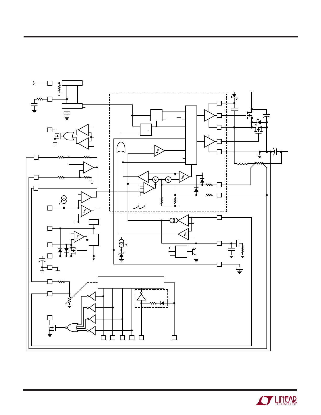
FU CTIO AL DIAGRA
f
IN
V
V
DIFFOUT
OS
OS
R
LP
C
LP
–
+
5V
+
PLLIN
PLLFLTR
PGOOD
FCB
V
EXTV
INTV
SGND
ATTENIN
ATTENOUT
0.18µA
IN
CC
CC
50k
PHASE DET
OSCILLATOR
40k
40k
3V
4.8V
10k
0.60V
4.5V
R1
CLK1
CLK2
TO SECOND
CHANNEL
–
0.66V
+
EAIN
–
+
0.54V
40k
–
A1
+
40k
–
+
+
FCB
–
V
REF
+
–
5V
LDO
REG
INTERNAL
SUPPLY
DUPLICATE FOR SECOND
CONTROLLER CHANNEL
0.86V
5V
FB
SLOPE
COMP
1.2µA
6V
5-BIT VID DECODER
SRQ
0.55V
I
1
DROP
OUT
DET
Q
+
–
–
+
45k
TYPICAL ALL
VID PINS
40k
B
+–
SHDN
BOT FCB
+–
RST
5V
FB
TOP ON
SHDN
–
+
45k
2.4V
OV
RUN
SOFT-
START
I
2
EA
SWITCH
LOGIC
–
+
+
–
INTV
BOOST
CC
INTV
30k
30k
CC
TG
SW
BG
PGND
SENSE
SENSE
EAIN
I
TH
RUN/SS
+
–
TOP
BOT
INTV
V
FB
0.60V
0.66V
V
CC
IN
D
B
C
B
L
C
C
C
R
C2
C
C
SS
R
D1
SENSE
+
C
IN
C
OUT
+
V
OUT
21
43
10
NO_CPU
VID0
VID1 VID2 VID3 VID4
V
BIAS
3719 FBD
sn3719 3719fs

OPERATIO
LTC3719
U
(Refer to Functional Diagram)
Main Control Loop
The LTC3719 uses a constant frequency, current mode
step-down architecture with the two output stages operating 180 degrees out of phase. During normal operation,
each top MOSFET is turned on when the clock for that
channel sets the RS latch, and turned off when the main
current comparator, I1, resets the RS latch. The peak
inductor current at which I1 resets the RS latch is controlled by the voltage on the I
error amplifier EA. The EAIN pin receives the voltage
feedback signal, which is compared to the internal reference voltage by the EA. When the load current increases,
it causes a slight decrease in V
reference, which in turn causes the ITH voltage to increase
until the average inductor current matches the new load
current. After the top MOSFET has turned off, the bottom
MOSFET is turned on until either the inductor current
starts to reverse, as indicated by current comparator I2, or
the beginning of the next cycle.
The top MOSFET drivers are biased from floating bootstrap capacitor CB, which normally is recharged during
each off cycle through an external diode when the top
MOSFET turns off. As VIN decreases to a voltage close to
V
, the loop may enter dropout and attempt to turn on
OUT
the top MOSFET continuously. The dropout detector detects this and forces the top MOSFET off for about 500ns
every tenth cycle to allow CB to recharge.
The main control loop is shut down by pulling the RUN/
SS pin low. Releasing RUN/SS allows an internal 1.2µA
current source to charge soft-start capacitor CSS. When
CSS reaches 1.5V, the main control loop is enabled with
the ITH voltage clamped at approximately 30% of its
maximum value. As CSS continues to charge, the I
voltage is gradually released allowing normal, full-current
operation.
Low Current Operation
The FCB pin selects between
operation. When the FCB pin voltage is below 0.6V, the
controller forces continuous PWM current mode opera-
pin, which is the output of
TH
relative to the 0.6V
EAIN
TH
two
modes of low current
pin
tion. In this mode, the top and bottom MOSFETs are
alternately turned on to maintain the output voltage
independent of direction of inductor current. When the
FCB pin is below V
controller enters Burst Mode operation. Burst Mode
operation sets a minimum output current level before
inhibiting the top switch and turns off the synchronous
MOSFET(s) when the inductor current goes negative.
This combination of requirements will, at low currents,
force the ITH pin below a voltage threshold that will
temporarily inhibit turn-on of both output MOSFETs until
the output voltage drops. There is 60mV of hysteresis in
the burst comparator B tied to the ITH pin. This hysteresis
produces output signals to the MOSFETs that turn them
on for several cycles, followed by a variable “sleep”
interval depending upon the load current. The resultant
output voltage ripple is held to a very small value by
having the hysteretic comparator after the error amplifier
gain block.
Constant Frequency Operation
When the FCB pin is tied to INTVCC, Burst Mode operation
is disabled and a forced minimum peak output current
requirement is removed. This provides constant frequency,
discontinuous (preventing reverse inductor current) current operation over the widest possible output current
range. This constant frequency operation is not as efficient
as Burst Mode operation, but does provide a lower noise,
constant frequency operating mode down to approximately 1% of designed maximum output current.
Continuous Current (PWM) Operation
Tying the FCB pin to ground will force continuous current
operation. This is the least efficient operating mode, but
may be desirable in certain applications. The output can
source or sink current in this mode. When sinking current
while in forced continuous operation, current will be
forced back into the main power supply potentially boosting the input supply to dangerous voltage levels—
BEWARE!
␣ –␣ 2V but greater than 0.6V, the
INTVCC
sn3719 3719fs
11

LTC3719
OPERATIO
U
(Refer to Functional Diagram)
Frequency Synchronization
The phase-locked loop allows the internal oscillator to be
synchronized to an external source via the PLLIN pin. The
output of the phase detector at the PLLFLTR pin is also the
DC frequency control input of the oscillator that operates
over a 140kHz to 310kHz range corresponding to a DC
voltage input from 0V to 2.4V. When locked, the PLL aligns
the turn on of the top MOSFET to the rising edge of the
synchronizing signal. When PLLIN is left open, the PLLFLTR
pin goes low, forcing the oscillator to minimum frequency.
Input capacitance ESR requirements and efficiency losses
are substantially reduced because the peak current drawn
from the input capacitor is effectively divided by two and
power loss is proportional to the RMS current squared. A
two stage, single output voltage implementation can
reduce input path power loss by 75% and radically reduce
the required RMS current rating of the input capacitor(s).
INTVCC/EXTVCC Power
Power for the top and bottom MOSFET drivers and most
of the IC circuitry is derived from INTVCC. When the
EXTVCC pin is left open, an internal 5V low dropout
regulator supplies INTVCC power. If the EXTVCC pin is
taken above 4.8V, the 5V regulator is turned off and an
internal switch is turned on connecting EXTVCC to INTVCC.
This allows the INTVCC power to be derived from a high
efficiency external source such as the output of the regulator itself or a secondary winding, as described in the
Applications Information section. An external Schottky
diode can be used to minimize the voltage drop from
EXTVCC to INTV
the specified INTVCC current. Voltages up to 7V can be
applied to EXTVCC for additional gate drive capability.
Differential Amplifier
This controller includes a true unity-gain differential amplifier. Sensing both V
lation in high current applications and/or applications
having electrical interconnection losses. The amplifier is
a unity-gain stable, 2MHz gain-bandwidth, >120dB openloop gain design. The amplifier has an output slew rate of
5V/µs and is capable of driving capacitive loads with an
in applications requiring greater than
CC
OUT
+
and V
–
benefits regu-
OUT
output RMS current typically up to 25mA. The amplifier
is not capable of sinking current and therefore must be
resistively loaded to do so.
Output Overvoltage Protection
An overvoltage comparator, 0V, guards against transient
overshoots (>10%) as well as other more serious conditions that may overvoltage the output. In this case, the top
MOSFET is turned off and the bottom MOSFET is turned on
until the overvoltage condition is cleared.
Power Good (PGOOD)
The PGOOD pin is connected to the drain of an internal
MOSFET. The MOSFET turns on when the output voltage
is not within ±10% of its nominal output level as determined by the feedback divider. When the output is within
±10% of its nominal value, the MOSFET is turned off within
10µs and the PGOOD pin should be pulled up by an
external resistor to a source of up to 7V.
Short-Circuit Detection
The RUN/SS capacitor is used initially to limit the inrush
current from the input power source. Once the controllers have been given time, as determined by the capacitor
on the RUN/SS pin, to charge up the output capacitors
and provide full-load current, the RUN/SS capacitor is
then used as a short-circuit timeout circuit. If the output
voltage falls to less than 70% of its nominal output
voltage the RUN/SS capacitor begins discharging assuming that the output is in a severe overcurrent and/or
short-circuit condition. If the condition lasts for a long
enough period as determined by the size of the RUN/SS
capacitor, the controller will be shut down until the
RUN/SS pin voltage is recycled. This built-in latchoff can
be overidden by providing a current >5µA at a compli-
ance of 5V to the RUN/SS pin. This current shortens the
soft-start period but also prevents net discharge of the
RUN/SS capacitor during a severe overcurrent and/or
short-circuit condition. Foldback current limiting is activated when the output voltage falls below 70% of its
nominal level whether or not the short-circuit latchoff
circuit is enabled.
12
sn3719 3719fs

LTC3719
OPERATING FREQUENCY (kHz)
120 170 220 270 320
PLLFLTR PIN VOLTAGE (V)
3719 F02
2.5
2.0
1.5
1.0
0.5
0
U
WUU
APPLICATIO S I FOR ATIO
The basic LTC3719 application circuit is shown in
Figure␣ 1 on the first page. External component selection
begins with the selection of the inductors based on ripple
current requirements and continues with the current
sensing resistors using the calculated peak inductor
current and/or maximum current limit. Next, the power
MOSFETs, D1 and D2 are selected. The operating frequency and the inductor are chosen based mainly on the
amount of ripple current. Finally, CIN is selected for its
ability to handle the input ripple current (that PolyPhase
operation minimizes) and C
is chosen with low enough
OUT
ESR to meet the output ripple voltage and load step
specifications (also minimized with PolyPhase). Current
mode architecture provides inherent current sharing between output stages. The circuit shown in Figure␣ 1 can be
configured for operation up to an input voltage of 28V
(limited by the external MOSFETs). Current mode control
allows the ability to connect the two output stages to two
different
take some power from
selection of the R
input power supply rails. A heavy output load can
each
input supply according to the
resistors.
SENSE
TM
plus an additional current which is proportional to the
voltage applied to the PLLFLTR pin. Refer to PhaseLocked Loop and Frequency Synchronization for additional information.
A graph for the voltage applied to the PLLFLTR pin vs
frequency is given in Figure␣ 2. As the operating frequency
is increased the gate charge losses will be higher, reducing
efficiency (see Efficiency Considerations). The maximum
switching frequency is approximately 310kHz.
R
SENSE
R
SENSE1,2
current. The LTC3719 current comparator has a maximum threshold of 75mV/R
mode range of SGND to 1.1(INTVCC). The current comparator threshold sets the peak inductor current, yielding
a maximum average output current I
value less half the peak-to-peak ripple current, ∆IL.
Assuming a common input power source for each output
stage and allowing a margin for variations in the
LTC3719 and external component values yields:
RN
SENSE
where N = 2 for 2 phase. For more than 2 phase use the
LTC1629-6 plus the LTC3719.
Operating Frequency
The LTC3719 uses a constant frequency, phase-lockable
architecture with the frequency determined by an internal
capacitor. This capacitor is charged by a fixed current
Selection For Output Current
are chosen based on the required peak output
and an input common
SENSE
equal to the peak
MAX
mV
50
=
I
MAX
Figure 2. Operating Frequency vs V
PLLFLTR
Inductor Value Calculation and Output Ripple Current
The operating frequency and inductor selection are interrelated in that higher operating frequencies allow the use
of smaller inductor and capacitor values. So why would
anyone ever choose to operate at lower frequencies with
larger components? The answer is efficiency. A higher
frequency generally results in lower efficiency because
MOSFET gate charge and transition losses increase
directly with frequency. In addition to this basic tradeoff,
the effect of inductor value on ripple current and low
current operation must also be considered. The PolyPhase
approach reduces both input and output ripple currents
while optimizing individual output stages to run at a lower
fundamental frequency, enhancing efficiency.
The inductor value has a direct effect on ripple current.
The inductor ripple current ∆IL per individual section, N,
decreases with higher inductance or frequency and
increases with higher VIN or V
PolyPhase is a registered trademark of Linear Technology Corporation.
OUT
:
sn3719 3719fs
13

LTC3719
U
WUU
APPLICATIO S I FOR ATIO
V
OUT OUT
•
fL
1
∆I
=−
L
where f is the individual output stage operating frequency.
In a 2-phase converter, the net ripple current seen by the
output capacitor is much smaller than the individual
inductor ripple currents due to ripple cancellation. The
details on how to calculate the net output ripple current
can be found in Application Note 77.
Figure 3 shows the net ripple current seen by the output
capacitors for 1- and 2-phase configurations. The output
ripple current is plotted for a fixed output voltage as the
duty factor is varied between 10% and 90% on the x-axis.
The output ripple current is normalized against the inductor ripple current at zero duty factor. The graph can be
used in place of tedious calculations, simplifying the
design process.
1.0
0.9
0.8
0.7
0.6
/fL
0.5
O
O(P-P)
V
∆I
0.4
0.3
0.2
0.1
0
0.1 0.2 0.3 0.4
Figure 3. Normalized Output Ripple Current
vs Duty Factor [I
Accepting larger values of ∆IL allows the use of low
inductances, but can result in higher output voltage ripple.
A reasonable starting point for setting ripple current is
∆IL = 0.4(I
)/2, where I
OUT
Remember, the maximum ∆IL occurs at the maximum
input voltage. The individual inductor ripple currents are
determined by the inductor, input and output voltages.
V
V
IN
DUTY FACTOR (V
0.5 0.6 0.7 0.8 0.9
≈ 0.3 (∆I
RMS
OUT
1-PHASE
2-PHASE
)
OUT/VIN
O(P–P)
3719 F03
)]
is the total load current.
generally cannot afford the core loss found in low cost
powdered iron cores, forcing the use of more expensive
ferrite, molypermalloy, or Kool Mµ® cores. Actual core
loss is independent of core size for a fixed inductor value,
but it is very dependent on inductor type selected. As
inductance increases, core losses go down. Unfortunately, increased inductance requires more turns of wire
and therefore copper losses will increase.
Ferrite designs have very low core loss and are preferred
at high switching frequencies, so design goals can concentrate on copper loss and preventing saturation. Ferrite
core material saturates “hard,” which means that inductance collapses abruptly when the peak design current is
exceeded. This results in an abrupt increase in inductor
ripple current and consequent output voltage ripple.
Do
not allow the core to saturate!
Molypermalloy (from Magnetics, Inc.) is a very good, low
loss core material for toroids, but it is more expensive
than ferrite. A reasonable compromise from the same
manufacturer is Kool Mµ. Toroids are very space efficient, especially when you can use several layers of wire.
Because they lack a bobbin, mounting is more difficult.
However, designs for surface mount are available which
do not increase the height significantly.
Power MOSFET, D1 and D2 Selection
Two external power MOSFETs must be selected for each
output stage with the LTC3719: one N-channel MOSFET
for the top (main) switch, and one N-channel MOSFET for
the bottom (synchronous) switch.
The peak-to-peak drive levels are set by the INTV
CC
voltage. This voltage is typically 5V during start-up
(see EXTVCC Pin Connection). Consequently, logic-level
threshold MOSFETs must be used in most applications.
The only exception is if low input voltage is expected
(VIN < 5V); then, sublogic-level threshold MOSFETs
(V
BV
< 1V) should be used. Pay close attention to the
GS(TH)
specification for the MOSFETs as well; most of the
DSS
logic-level MOSFETs are limited to 30V or less.
Inductor Core Selection
Once the values for L1 and L2 are known, the type of
inductor must be selected. High efficiency converters
14
Selection criteria for the power MOSFETs include the “ON”
resistance R
, reverse transfer capacitance C
DS(ON)
RSS
,
input voltage and maximum output current. When the
Kool Mµ is a registered trademark of Magnetics, Inc.
sn3719 3719fs

LTC3719
U
WUU
APPLICATIO S I FOR ATIO
LTC3719 is operating in continuous mode the duty factors
for the top and bottom MOSFETs of each output stage are
given by:
V
Main SwitchDuty Cycle
Synchronous SwitchDuty Cycle
The MOSFET power dissipations at maximum output
current are given by:
V
P
MAIN
P
SYNC
where δ is the temperature dependency of R
is a constant inversely related to the gate drive current.
Both MOSFETs have I2R losses but the topside N-channel
equation includes an additional term for transition losses,
which peak at the highest input voltage. For V
high current efficiency generally improves with larger
MOSFETs, while for V
increase to the point that the use of a higher R
with lower C
synchronous MOSFET losses are greatest at high input
voltage when the top switch duty factor is low or during a
short-circuit when the synchronous switch is on close to
100% of the period.
The term (1 + δ) is generally given for a MOSFET in the
form of a normalized R
δ = 0.005/°C can be used as an approximation for low
voltage MOSFETs. C
MOSFET characteristics. The constant k = 1.7 can be
used to estimate the contributions of the two terms in the
main switch dissipation equation.
OUTINMAX
=
V
2
kV
IN
()
VVVI
–
IN OUTINMAX
=
actual provides higher efficiency. The
RSS
I
2
I
MAX
2
> 20V the transition losses rapidly
IN
DS(ON)
RSS
OUT
=
V
IN
VV
–
IN OUT
=
V
2
1
R
+
δ
()
Cf
RSS
()()
2
is usually specified in the
DS ON
2
1
+
()
vs temperature curve, but
()
R
δ
DS ON
+
()
DS(ON)
IN
DS(ON)
IN
and k
< 20V the
device
The Schottky diodes, D1 and D2 shown in Figure 1
conduct during the dead-time between the conduction of
the two large power MOSFETs. This helps prevent the
body diode of the bottom MOSFET from turning on,
storing charge during the dead-time, and requiring a
reverse recovery period which would reduce efficiency. A
1A to 3A Schottky (depending on output current) diode is
generally a good compromise for both regions of operation due to the relatively small average current. Larger
diodes result in additional transition losses due to their
larger junction capacitance.
CIN and C
In continuous mode, the source current of each top
N-channel MOSFET is a square wave of duty cycle V
VIN. A low ESR input capacitor sized for the maximum
RMS current must be used. The details of a closed form
equation can be found in Application Note 77. Figure 4
shows the input capacitor ripple current for a 2-phase
configuration with the output voltage fixed and input
voltage varied. The input ripple current is normalized
against the DC output current. The graph can be used in
place of tedious calculations. The minimum input ripple
current can be achieved when the input voltage is twice the
output voltage.
In the graph of Figure 4, the 2-phase local maximum input
RMS capacitor currents are reached when:
V
OUT
V
IN
where k = 1, 2
These worst-case conditions are commonly used for
design because even significant deviations do not offer
much relief. Note that capacitor manufacturer’s ripple
current ratings are often based on only 2000 hours of life.
This makes it advisable to further derate the capacitor, or
to choose a capacitor rated at a higher temperature than
required. Several capacitors may also be paralleled to
meet size or height requirements in the design. Always
consult the capacitor manufacturer if there is any
question.
Selection
OUT
k
=
4
−21
OUT
sn3719 3719fs
/
15

LTC3719
U
WUU
APPLICATIO S I FOR ATIO
0.6
0.5
0.4
0.3
0.2
DC LOAD CURRENT
RMS INPUT RIPPLE CURRNET
0.1
0
0.1 0.2 0.3 0.4 0.5 0.6 0.7 0.8
Figure 4. Normalized RMS Input Ripple Current
vs Duty Factor for 1 and 2 Output Stages
DUTY FACTOR (V
It is important to note that the efficiency loss is proportional to the input RMS current
2-phase implementation results in 75% less power loss
when compared to a single phase design. Battery/input
protection fuse resistance (if used), PC board trace and
connector resistance losses are also reduced by the
reduction of the input ripple current in a 2-phase system.
The required amount of input capacitance is further
reduced by the factor, 2, due to the effective increase in
the frequency of the current pulses.
The selection of C
is driven by the required effective
OUT
series resistance (ESR). Typically once the ESR requirement has been met, the RMS current rating generally far
exceeds the I
output ripple (∆V
RIPPLE(P-P)
) is determined by:
OUT
∆∆V I ESR
≈+
OUT RIPPLE
Where f = operating frequency of each stage, C
output capacitance and ∆I
ripple currents.
The output ripple varies with input voltage since ∆IL is a
function of input voltage. The output ripple will be less than
50mV at max VIN with ∆IL = 0.4I
1-PHASE
2-PHASE
0.9
)
OUT/VIN
squared
3719 F04
and therefore a
requirements. The steady state
1
fC
16
RIPPLE
OUT(MAX)
OUT
=
OUT
= combined inductor
/2 assuming:
C
C
required ESR < 4(R
OUT
> 1/(16f)(R
OUT
SENSE
)
SENSE
) and
The emergence of very low ESR capacitors in small,
surface mount packages makes very physically small
implementations possible. The ability to externally compensate the switching regulator loop using the I
TH
pin(OPTI-LOOP compensation) allows a much wider selection of output capacitor types. OPTI-LOOP compensation effectively removes constraints on output capacitor
ESR. The impedance characteristics of each capacitor
type are significantly different than an ideal capacitor and
therefore require accurate modeling or bench evaluation
during design.
Manufacturers such as Nichicon, United Chemicon and
Sanyo should be considered for high performance
through-hole capacitors. The OS-CON semiconductor
dielectric capacitor available from Sanyo and the Panasonic
SP surface mount types have the lowest (ESR)(size)
product of any aluminum electrolytic at a somewhat
higher price. An additional ceramic capacitor in parallel
with OS-CON type capacitors is recommended to reduce
the inductance effects.
In surface mount applications, multiple capacitors may
have to be paralleled to meet the ESR or RMS current
handling requirements of the application. Aluminum electrolytic and dry tantalum capacitors are both available in
surface mount configurations. New special polymer surface mount capacitors offer very low ESR also but have
much lower capacitive density per unit volume. In the case
of tantalum, it is critical that the capacitors are surge tested
for use in switching power supplies. Several excellent
choices are the AVX TPS, AVX TPSV or the KEMET T510
series of surface mount tantalums, available in case heights
ranging from 2mm to 4mm. Other capacitor types include
Sanyo OS-CON, POSCAPs, Panasonic SP caps, Nichicon
PL series and Sprague 595D series. Consult the manufacturer for other specific recommendations. A combination
of capacitors will often result in maximizing performance
and minimizing overall cost and size.
16
sn3719 3719fs

LTC3719
U
WUU
APPLICATIO S I FOR ATIO
INTVCC Regulator
An internal P-channel low dropout regulator produces 5V
at the INTVCC pin from the VIN supply pin. The INTV
regulator powers the drivers and internal circuitry of the
LTC3719. The INTVCC pin regulator can supply up to 50mA
peak and must be bypassed to power ground with a
minimum of 4.7µF tantalum or electrolytic capacitor. An
additional 1µF ceramic capacitor placed very close to the
IC is recommended due to the extremely high instantaneous currents required by the MOSFET gate drivers.
High input voltage applications in which large MOSFETs
are being driven at high frequencies may cause the maximum junction temperature rating for the LTC3719 to be
exceeded. The supply current is dominated by the gate
charge supply current, in addition to the current drawn
from the differential amplifier output. The gate charge is
dependent on operating frequency as discussed in the
Efficiency Considerations section. The supply current can
either be supplied by the internal 5V regulator or via the
EXTVCC pin. When the voltage applied to the EXTVCC pin
is less than 4.7V, all of the INTVCC load current is supplied
by the internal 5V linear regulator. Power dissipation for
the IC is higher in this case by (IIN)(VIN – INTVCC) and
efficiency is lowered. The junction temperature can be
estimated by using the equations given in Note 1 of the
Electrical Characteristics. For example, the LTC3719 V
current is limited to less than 24mA from a 24V supply:
TJ = 70°C + (24mA)(24V)(85°C/W) = 119°C
Use of the EXTVCC pin reduces the junction temperature␣ to:
TJ = 70°C + (24mA)(5V)(85°C/W) = 80.2°C
The input supply current should be measured while the
controller is operating in continuous mode at maximum
V
and the power dissipation calculated in order to
IN
prevent the maximum junction temperature from being
exceeded.
EXTVCC Connection
CC
IN
When the voltage applied to EXTV
internal regulator is turned off and an internal switch
closes, connecting the EXTV
thereby supplying internal and MOSFET gate driving power
to the IC. The switch remains closed as long as the voltage
applied to EXTVCC remains above 4.5V. This allows the
MOSFET driver and control power to be derived from a
separate 5V supply during normal operation (4.7V <
V
EXTVCC
external 5V supply is not available. Do not apply greater
than 7V to the EXTVCC pin and ensure that EXTV
0.3V when using the application circuits shown. If an
external voltage source is applied to the EXTVCC pin when
the VIN supply is not present, a diode can be placed in
series with the LTC3719’s V
between the EXTV
from backfeeding VIN.
Topside MOSFET Driver Supply (CB,DB) (Refer to
Functional Diagram)
External bootstrap capacitors CB1 and CB2 connected to
the BOOST1 and BOOST2 pins supply the gate drive
voltages for the topside MOSFETs. Capacitor CB in the
Functional Diagram is charged though diode DB from
INTVCC when the SW pin is low. When the topside MOSFET
turns on, the driver places the CB voltage across the gatesource of the desired MOSFET. This enhances the MOSFET
and turns on the topside switch. The switch node voltage,
SW, rises to VIN and the BOOST pin rises to VIN + V
The value of the boost capacitor CB needs to be 30 to 100
times that of the total input capacitance of the topside
MOSFET(s). The reverse breakdown of DB must be greater
than V
The final arbiter when defining the best gate drive amplitude level will be the input supply current. If a change is
made that decreases input current, the efficiency has
improved. If the input current does not change then the
efficiency has not changed either.
< 7V) and from the internal regulator when the
IN
and the V
CC
IN(MAX).
rises above 4.7V, the
CC
pin to the INTV
CC
pin and a Schottky diode
pin, to prevent current
IN
CC
pin
CC
< V
IN
INTVCC
+
.
The LTC3719 contains an internal P-channel MOSFET
switch connected between the EXTVCC and INTVCC pins.
sn3719 3719fs
17

LTC3719
U
WUU
APPLICATIO S I FOR ATIO
Output Voltage
The LTC3719 has a true remote voltage sense capablity.
The sensing connections should be returned from the load
back to the differential amplifier’s inputs through a common, tightly coupled pair of PC traces. The differential
amplifier corrects for DC drops in both the power and
ground paths. The differential amplifier output signal is
divided down and compared with the internal precision
0.6V voltage reference by the error amplifier.
Output Voltage Programming
The output voltage is digitally programmed as defined in
Table 1 using the VID0 to VID4 logic input pins. The VID
logic inputs program a precision, 0.25% internal feedback
resistive divider. The LTC3719 has an output voltage range
of 0.8V to 1.55V in 25mV steps.
Between the ATTENOUT pin and ground is a variable
resistor, R1, whose value is controlled by the five VID input
pins (VID0 to VID4). Another resistor, R2, between the
ATTENIN and the ATTENOUT pins completes the resistive
divider. The output voltage is thus set by the ratio of
(R1␣ +␣ R2) to R1.
Each VID digital input is pulled up by a 40k resistor in series
with a diode from V
get a digital low input, and can be either floated or connected to V
to get a digital high input. The series diode
BIAS
is used to prevent the digital inputs from being damaged
or clamped if they are driven higher than V
inputs accept CMOS voltage levels.
V
is the supply voltage for the VID section. It is
BIAS
normally connected to INTVCC but can be driven from
other sources. If it is driven from another source, that
source
must
be in the range of 2.7V to 5.5V and
alive prior to enabling the LTC3719.
. Therefore, it must be grounded to
BIAS
. The digital
BIAS
must
be
Table 1. VID Output Voltage Programming
CODE VID4 VID3 VID2 VID1 VID0 OUTPUT
00000 GND GND GND GND GND 1.550
00001 GND GND GND GND Float 1.525
00010 GND GND GND Float GND 1.500
00011 GND GND GND Float Float 1.475
00100 GND GND Float GND GND 1.450
00101 GND GND Float GND Float 1.425
00110 GND GND Float Float GND 1.400
00111 GND GND Float Float Float 1.375
01000 GND Float GND GND GND 1.350
01001 GND Float GND GND Float 1.325
01010 GND Float GND Float GND 1.300
01011 GND Float GND Float Float 1.275
01100 GND Float Float GND GND 1.250
01101 GND Float Float GND Float 1.225
01110 GND Float Float Float GND 1.200
01111 GND Float Float Float Float 1.175
10000 Float GND GND GND GND 1.150
10001 Float GND GND GND Float 1.125
10010 Float GND GND Float GND 1.100
10011 Float GND GND Float Float 1.075
10100 Float GND Float GND GND 1.050
10101 Float GND Float GND Float 1.025
10110 Float GND Float Float GND 1.000
10111 Float GND Float Float Float 0.975
11000 Float Float GND GND GND 0.950
11001 Float Float GND GND Float 0.925
11010 Float Float GND Float GND 0.900
11011 Float Float GND Float Float 0.875
11100 Float Float Float GND GND 0.850
11101 Float Float Float GND Float 0.825
11110 Float Float Float Float GND 0.800
11111 Float Float Float Float Float Shutdown
18
sn3719 3719fs

LTC3719
U
WUU
APPLICATIO S I FOR ATIO
Soft-Start/Run Function
The RUN/SS pin provides three functions: 1) Run/Shutdown, 2) soft-start and 3) a defeatable short-circuit latchoff
timer. Soft-start reduces the input power sources’ surge
currents by gradually increasing the controller’s current
limit I
TH(MAX)
extreme load transients from tripping the overcurrent
latch. A small pull-up current (>5µA) supplied to the RUN/
SS pin will prevent the overcurrent latch from operating.
The following explanation describes how the functions
operate.
An internal 1.2µA current source charges up the soft-start
capacitor, CSS. When the voltage on RUN/SS reaches
1.5V, the controller is permitted to start operating. As the
voltage on RUN/SS increases from 1.5V to 3.0V, the
internal current limit is increased from 25mV/R
75mV/R
taking an additional 1.4s/µF to reach full current. The
output current thus ramps up slowly, reducing the starting
surge current required from the input power supply. If
RUN/SS has been pulled all the way to ground there is a
delay before starting of approximately:
t
DELAY SS SS
. The latchoff timer prevents very short,
. The output current limit ramps up slowly,
SENSE
15
.
=
12
.
V
CsFC
A
µ
125
./
=µ
()
SENSE
to
D1*
INTV
CC
RSS*
RUN/SS
C
3719 F06
SS
V
3.3V OR 5V RUN/SS
*OPTIONAL TO DEFEAT OVERCURRENT LATCHOFF
IN
RSS*
D1
C
SS
Figure 5. RUN/SS Pin Interfacing
Fault Conditions: Overcurrent Latchoff
The RUN/SS pin also provides the ability to latch off the
controllers when an overcurrent condition is detected. The
RUN/SS capacitor, CSS, is used initially to limit the inrush
current of both controllers. After the controllers have been
started and been given adequate time to charge up the
output capacitors and provide full load current, the RUN/
SS capacitor is used for a short-circuit timer. If the output
voltage falls to less than 70% of its nominal value after C
SS
reaches 4.1V, CSS begins discharging on the assumption
that the output is in an overcurrent condition. If the
condition lasts for a long enough period as determined by
the size of the CSS, the controller will be shut down until the
RUN/SS pin voltage is recycled. If the overload occurs
during start-up, the time can be approximated by:
The time for the output current to ramp up is then:
315
.
VV
t
IRAMP SS SS
−
=
12
.
CsFC
A
µ
125
./
=µ
()
By pulling the RUN/SS pin below 0.8V the LTC3719 is put
into low current shutdown (IQ < 40µA). The RUN/SS pins
can be driven directly from logic as shown in Figure 5.
Diode D1 in Figure 5 reduces the start delay but allows
CSS to ramp up slowly providing the soft-start function.
The RUN/SS pin has an internal 6V zener clamp (see
Functional Diagram).
t
≈ (CSS • 0.6V)/(1.2µA) = 5 • 105 (CSS)
LO1
If the overload occurs after start-up, the voltage on CSS will
continue charging and will provide additional time before
latching off:
t
≈ (CSS • 3V)/(1.2µA) = 2.5 • 106 (CSS)
LO2
This built-in overcurrent latchoff can be overridden by
providing a pull-up resistor, RSS, to the RUN/SS pin as
shown in Figure 5. This resistance shortens the soft-start
period and prevents the discharge of the RUN/SS capacitor during a severe overcurrent and/or short-circuit
sn3719 3719fs
19

LTC3719
U
WUU
APPLICATIO S I FOR ATIO
condi
tion. When deriving the 5µA current from VIN as in
the figure, current latchoff is always defeated. The diode
connecting this pull-up resistor to INTVCC, as in Figure␣ 5,
eliminates any extra supply current during shutdown
while eliminating the INTV
controller start-up.
Why should you defeat current latchoff? During the
prototyping stage of a design, there may be a problem with
noise pickup or poor layout causing the protection circuit
to latch off the controller. Defeating this feature allows
troubleshooting of the circuit and PC layout. The internal
short-circuit and foldback current limiting still remains
active, thereby protecting the power supply system from
failure. A decision can be made after the design is complete whether to rely solely on foldback current limiting or
to enable the latchoff feature by removing the pull-up
resistor.
The value of the soft-start capacitor CSS may need to be
scaled with output voltage, output capacitance and load
current characteristics. The minimum soft-start capacitance is given by:
CSS > (C
OUT
)(V
)(10-4)(R
OUT
The minimum recommended soft-start capacitor of CSS =
0.1µF will be sufficient for most applications.
Phase-Locked Loop and Frequency Synchronization
The LTC3719 has a phase-locked loop comprised of an
internal voltage controlled oscillator and phase detector.
This allows the top MOSFET turn-on to be locked to the
rising edge of an external source. The frequency range of
the voltage controlled oscillator is ±50% around the
center frequency fO. A voltage applied to the PLLFLTR pin
of 1.2V corresponds to a frequency of approximately
220kHz. The nominal operating frequency range of the
LTC3719 is 140kHz to 310kHz.
The phase detector used is an edge sensitive digital type
which provides zero degrees phase shift between the
loading from preventing
CC
)
SENSE
external and internal oscillators. This type of phase detector will not lock up on input frequencies close to the
harmonics of the VCO center frequency. The PLL hold-in
range, ∆fH, is equal to the capture range, ∆f
C:
∆fH = ∆fC = ±0.5 fO (150kHz-300kHz)
The output of the phase detector is a complementary pair
of current sources charging or discharging the external
filter network on the PLLFLTR pin. A simplified block
diagram is shown in Figure 6.
PHASE
50k
DETECTOR
DIGITAL
PHASE/
FREQUENCY
DETECTOR
EXTERNAL
OSC
PLLIN
Figure 6. Phase-Locked Loop Block Diagram
If the external frequency (f
lator frequency f
, current is sourced continuously,
0SC
2.4V
) is greater than the oscil-
PLLIN
R
LP
10k
PLLFLTR
3719 F07
OSC
C
LP
pulling up the PLLFLTR pin. When the external frequency
is less than f
, current is sunk continuously, pulling
0SC
down the PLLFLTR pin. If the external and internal frequencies are the same but exhibit a phase difference, the
current sources turn on for an amount of time corresponding to the phase difference. Thus the voltage on the
PLLFLTR pin is adjusted until the phase and frequency of
the external and internal oscillators are identical. At this
stable operating point the phase comparator output is
open and the filter capacitor CLP holds the voltage. The
LTC3719 PLLIN pin must be driven from a low impedance
source such as a logic gate located close to the pin.
20
sn3719 3719fs

LTC3719
U
WUU
APPLICATIO S I FOR ATIO
The loop filter components (CLP, RLP) smooth out the
current pulses from the phase detector and provide a
stable input to the voltage controlled oscillator. The filter
components CLP and RLP determine how fast the loop
acquires lock. Typically R
0.1µF.
Minimum On-Time Considerations
Minimum on-time, t
ON(MIN)
that the LTC3719 is capable of turning on the top MOSFET.
It is determined by internal timing delays and the gate
charge required to turn on the top MOSFET. Low duty cycle
applications may approach this minimum on-time limit
and care should be taken to ensure that:
V
t
ON MIN
()
<
Vf
IN
OUT
()
If the duty cycle falls below what can be accommodated by
the minimum on-time, the LTC3719 will begin to skip
cycles resulting in variable frequency operation. The output voltage will continue to be regulated, but the ripple
current and ripple voltage will increase.
The minimum on-time for the LTC3719 is generally less
than 200ns. However, as the peak sense voltage decreases, the minimum on-time gradually increases. This is
of particular concern in forced continuous applications
with low ripple current at light loads. If the duty cycle drops
below the minimum on-time limit in this situation, a
significant amount of cycle skipping can occur with correspondingly larger ripple current and voltage ripple.
If an application can operate close to the minimum
on-time limit, an inductor must be chosen that has a low
enough inductance to provide sufficient ripple amplitude
to meet the minimum on-time requirement.
rule, keep the inductor ripple current of each phase equal
to or greater than 15% of I
=10k and CLP is 0.01µF to
LP
, is the smallest time duration
As a general
OUT(MAX)
at V
IN(MAX)
.
FCB Pin Operation
The following table summarizes the possible states available on the FCB pin:
Table 2
FCB Pin Condition
0V to 0.55V Forced Continuous (Current Reversal
0.65V < V
>4.8V Burst Mode Operation Disabled
< 4.3V (typ) Minimum Peak Current Induces
FCB
Allowed—Burst Inhibited)
Burst Mode Operation
No Current Reversal Allowed
Constant Frequency Mode Enabled
No Current Reversal Allowed
No Minimum Peak Current
Active Voltage Positioning
Active voltage positioning can be used to minimize peakto-peak output voltage excursion under worst-case transient loading conditions. The open-loop DC gain of the
control loop is reduced depending upon the maximum
load step specifications. Active voltage positioning can
easily be added to the LTC3719 by loading the ITH pin with
a resistive divider having a Thevenin equivalent voltage
source equal to the midpoint operating voltage of the error
amplifier, or 1.2V (see Figure 7).
The resistive load reduces the DC loop gain while maintaining the linear control range of the error amplifier. The
worst-case peak-to-peak output voltage deviation due to
transient loading can theoretically be reduced to half or
alternatively the amount of output capacitance can
be reduced for a particular application. A complete
explanation is included in Design Solutions 10 or the
LTC1736 data sheet. (See www.linear-tech.com)
INTV
CC
R
T2
I
TH
R
R
C
T1
C
C
LTC3719
3719 F08
Figure 7. Active Voltage Positioning Applied to the LTC3719
sn3719 3719fs
21

LTC3719
U
WUU
APPLICATIO S I FOR ATIO
Efficiency Considerations
The percent efficiency of a switching regulator is equal to
the output power divided by the input power times 100%.
It is often useful to analyze individual losses to determine
what is limiting the efficiency and which change would
produce the most improvement. Percent efficiency can be
expressed as:
%Efficiency = 100% – (L1 + L2 + L3 + ...)
where L1, L2, etc. are the individual losses as a percentage
of input power.
Although all dissipative elements in the circuit produce
losses, four main sources usually account for most of the
losses in LTC3719 circuits: 1) I2R losses, 2) Topside
MOSFET transition losses, 3) INTVCC regulator current
and 4) LTC3719 VIN current (including loading on the
differential amplifier output).
1) I2R losses are predicted from the DC resistances of the
fuse (if used), MOSFET, inductor, current sense resistor,
and input and output capacitor ESR. In continuous mode
the average output current flows through L and R
but is “chopped” between the topside MOSFET and the
synchronous MOSFET. If the two MOSFETs have approximately the same R
, then the resistance of one
DS(ON)
MOSFET can simply be summed with the resistances of L,
R
R
and ESR to obtain I2R losses. For example, if each
SENSE
= 10mΩ, RL = 10mΩ, and R
DS(ON)
= 5mΩ, then the
SENSE
total resistance is 25mΩ. This results in losses ranging
from 2% to 8% as the output current increases from 3A to
15A per output stage for a 5V output, or a 3% to 12% loss
per output stage for a 3.3V output. Efficiency varies as the
inverse square of V
for the same external components
OUT
and output power level. The combined effects of increasingly lower output voltages and higher currents required
by high performance digital systems is not doubling but
SENSE
,
quadrupling the importance of loss terms in the switching
regulator system!
2) Transition losses apply only to the topside MOSFET(s),
and are significant only when operating at high input
voltages (typically 12V or greater). Transition losses can
be estimated from:
Transition Loss V
=
(.)
17
IN
2
I
O MAX
()
2
Cf
RSS
3) INTVCC current is the sum of the MOSFET driver and
control currents. The MOSFET driver current results from
switching the gate capacitance of the power MOSFETs.
Each time a MOSFET gate is switched from low to high to
low again, a packet of charge dQ moves from INTVCC to
ground. The resulting dQ/dt is a current out of INTVCC that
is typically much larger than the control circuit current. In
continuous mode, I
GATECHG
= (QT + QB), where QT and Q
B
are the gate charges of the topside and bottom side
MOSFETs.
Supplying INTV
from an output-derived source will scale the V
power through the EXTVCC switch input
CC
current
IN
required for the driver and control circuits by the ratio
(Duty Factor)/(Efficiency). For example, in a 20V to 5V
application, 10mA of INTVCC current results in approximately 3mA of VIN current. This reduces the mid-current
loss from 10% or more (if the driver was powered directly
from VIN) to only a few percent.
4) The VIN current has two components: the first is the
DC supply current given in the Electrical Characteristics
table, which excludes MOSFET driver and control currents; the second is the current drawn from the differential
amplifier output. VIN current typically results in a small
(<0.1%) loss.
22
sn3719 3719fs

LTC3719
U
WUU
APPLICATIO S I FOR ATIO
Other “hidden” losses such as copper trace and internal
battery resistances can account for an additional 5% to
10% efficiency degradation in portable systems. It is very
important to include these “system” level losses in the
design of a system. The internal battery and input fuse
resistance losses can be minimized by making sure that
CIN has adequate charge storage and a very low ESR at
the switching frequency. A 50W supply will typically
require a minimum of 200µF to 300µF of output capaci-
tance having a maximum of 10mΩ to 20mΩ of ESR. The
LTC3719 2-phase architecture typically halves the input
and output capacitance requirements over competing
solutions. Other losses including Schottky conduction
losses during dead-time and inductor core losses generally account for less than 2% total additional loss.
Checking Transient Response
The regulator loop response can be checked by looking at
the load transient response. Switching regulators take
several cycles to respond to a step in DC (resistive) load
current. When a load step occurs, V
amount equal to ∆I
series resistance of C
discharge C
forces the regulator to adapt to the current change and
return V
time V
ringing, which would indicate a stability problem.
OUT
OUT
generating the feedback error signal that
OUT
to its steady-state value. During this recovery
can be monitored for excessive overshoot or
(ESR), where ESR is the effective
LOAD
OUT
(∆I
) also begins to charge or
LOAD
availability of the ITH pin not only allows optimization of
control loop behavior but also provides a DC coupled and
AC filtered closed loop response test point. The DC step,
rise time, and settling at this test point truly reflects the
closed loop response.
Assuming a predominantly second
shifts by an
OUT
The
order system, phase margin and/or damping factor can be
estimated using the percentage of overshoot seen at this
pin. The bandwidth can also be estimated by examining
the rise time at the pin. The ITH external components
shown in the Figure 1 circuit will provide an adequate
starting point for most applications.
The I
loop compensation. The values can be modified slightly
(from 0.2 to 5 times their suggested values) to optimize
transient response once the final PC layout is done and the
particular output capacitor type and value have been
determined. The output capacitors need to be decided
upon first because the various types and values determine
the loop gain and phase. An output current pulse of 20%
to 80% of full-load current having a rise time of <2µs will
produce output voltage and ITH pin waveforms that will
give a sense of the overall loop stability without breaking
the feedback loop. The initial output voltage step resulting
from the step change in output current may not be within
the bandwidth of the feedback loop, so this signal cannot
be used to determine phase margin. This is why it is
better to look at the Ith pin signal which is in the feedback
loop and is the filtered and compensated control loop
response. The gain of the loop will be increased by
increasing RC and the bandwidth of the loop will be
increased by decreasing CC. If RC is increased by the
same factor that CC is decreased, the zero frequency will
be kept the same, thereby keeping the phase the same in
the most critical frequency range of the feedback loop.
The output voltage settling behavior is related to the
stability of the closed-loop system and will demonstrate
the actual overall supply performance.
series RC-CC filter sets the dominant pole-zero
TH
sn3719 3719fs
23

LTC3719
DF
V
V
V
V
O
IN
== =
12
5
024..
WUUU
APPLICATIO S I FOR ATIO
Design Example
As a design example, assume VIN = 5V (nominal), VIN␣ =␣ 5.5V
(max), V
The inductance value is chosen first based on a 30% ripple
current assumption. The highest value of ripple current
occurs at the maximum input voltage. Tie the FREQSET pin
to the INTVCC pin for 300kHz operation. The minimum
inductance for 30% ripple current is:
L
≥
≥
≥µ
= 1.2V, I
OUT
V
OUT OUT
1
−
fL
∆
()
12
.
300 30 10
kHz A
()()()
104
.
H
= 20A, TA = 70°C and f␣ =␣ 300kHz.
MAX
V
V
IN
V
%
−
1
12
.
55
.
V
V
P
MAIN
The worst-case power disipated by the synchronous
MOSFET under normal operating conditions at elevated
ambient temperature and estimated 50°C junction temperature rise is:
P
SYNC
A short-circuit to ground will result in a folded back current
of about:
.
=
=
=
10 1 0 005 110 25
()+()
V
55
.
0 013 1 7 5 5 10 300
...
Ω
+
kHz W
300 0 45
()
55 12
..
15
.
=
VV
−
55
V
.
W
.
[]
2
VApF
()()( )
.
2 10 1 48 0 013
2
A
()()
°− °
()
..
()
CC
Ω
2
V
12
A 1µH inductor will produce 31% ripple current. The peak
inductor current will be the maximum DC value plus one
half the ripple current, or 11.5A. The minimum on-time
occurs at maximum VIN:
V
t
ON MIN
()
The R
SENSE
maximum current sense voltage specification with some
accomodation for tolerances:
R
SENSE
The power dissipation on the topside MOSFET can be
easily estimated. Using a Siliconix Si4420DY for example;
R
voltage with TJ (estimated) = 110°C at an elevated ambient
temperature:
= 0.013Ω, C
DS(ON)
OUT
==
Vf
IN
resistors value can be calculated by using the
mV
50
=≈Ω
11 5
.
5 5 300
()( )
0 004
.
A
RSS
V
12
.
V kHz
.
= 300pF. At maximum input
=µ
073
.
s
ns V
200 5 5
SC
SYNC
=
25
0 004
.
=
=
..
55 12
696
I
The worst-case power disipated by the synchronous
MOSFET under short-circuit conditions at elevated ambient temperature and estimated 50°C junction temperature
rise is:
P
which is less than normal, full-load conditions. Incidentally, since the load no longer dissipates power in the
shorted condition, total system power dissipation is decreased by over 99%.
The duty factor for this application is:
1
+
Ω
2
VV
−
.
V
55
mW
mV
()
µ
1
...
A
68 148 0013
()()
.
H
2
A
=
68
.
()
Ω
24
sn3719 3719fs

LTC3719
U
WUU
APPLICATIO S I FOR ATIO
Using Figure 4, the RMS ripple current will be:
I
= (20A)(0.25) = 5A
INRMS
An input capacitor(s) with a 5A
required.
The output capacitor ripple current is calculated by using
the inductor ripple already calculated for each inductor
and multiplying by the factor obtained from Figure␣ 3
along with the calculated duty factor. The output ripple in
con
tinuous mode will be highest at the maximum input
voltage since the duty factor is <50%. The maximum
output current ripple is:
V
OUT
05 24
∆∆I
VmAmV
OUTRIPPLE P P P P
=
COUT
I
COUTMAX
.%
()
fL
=
300 1 0
()
2
=
A
-
PP
20 2 40
=Ω
PC Board Layout Checklist
When laying out the printed circuit board, the following
checklist should be used to ensure proper operation of the
LTC3719. Check the following in your layout:
1) Are the signal and power grounds separate? The signal
ground traces should return to Pin 9 first. Connect Pin 9
to Pin 28 through a wide and straight trace. Then the signal
RMS
ripple current rating is
RMS
at D F
12
.
V
kHz H
()
--
()
05
.
.
µ
=
ground joins the power ground plane beside Pin 28. It is
recommended that the Pin 28 return to the (–) plates of CIN.
2) Does the LTC3719 V
load? Does the LTC3719 V
+
pin connect to the point of
OS
–
pin connect to the load
OS
return?
3) Are the SENSE– and SENSE+ leads routed together with
minimum PC trace spacing? The filter capacitors between
SENSE+ and SENSE– pin pairs should be as close as
possible to the LTC3719. Ensure accurate current sensing
with Kelvin connections at the current sense resistor. See
Figure 8.
4) Does the (+) plate of CIN connect to the drains of the
topside MOSFETs as closely as possible? This capacitor
provides the AC current to the MOSFETs. Keep the input
current path formed by the input capacitor, top and bottom
MOSFETs, and the Schottky diode on the same side of the
PC board in a tight loop to minimize conducted and
radiated EMI.
5) Is the INTVCC 1µF ceramic decoupling capacitor con-
nected closely between INTVCC and the PGND pin? This
capacitor carries the MOSFET driver peak currents. A
small value is recommended to allow placement immediately adjacent to the IC.
6) Keep the switching nodes, SW1 (SW2), away from
sensitive small-signal nodes. Ideally the switch nodes
should be placed at the furthest point from the
LTC3719.
7) Use a low impedance source such as a logic gate to drive
the PLLIN pin and keep the lead as short as possible.
PADS OF SENSE RESISTOR
TRACE TO INDUCTOR
+
SENSE
Figure 8. Proper Current Sense Connections
SENSE
–
TRACE TO OUTPUT CAP (+)
3719 F09
sn3719 3719fs
25

LTC3719
U
WUU
APPLICATIO S I FOR ATIO
The diagram in Figure 9 illustrates all branch currents in a
2-phase switching regulator. It becomes very clear after
studying the current waveforms why it is critical to keep
the high-switching-current paths to a small physical size.
High electric and magnetic fields will radiate from these
“loops” just as radio stations transmit signals. The output
capacitor ground should return to the negative terminal of
the input capacitor and not share a common ground path
with any switched current paths. The left half of the circuit
gives rise to the “noise” generated by a switching regulator. The ground terminations of the sychronous MOSFETs
and Schottky diodes should return to the negative plate(s)
SW1
of the input capacitor(s) with a short isolated PC trace
since very high switched currents are present. A separate
isolated path from the negative plate(s) of the input
capacitor(s) should be used to tie in the IC power ground
pin (PGND) and the signal ground pin (SGND). This
technique keeps inherent signals generated by high current pulses from taking alternate current paths that have
finite impedances during the total period of the switching
regulator. External OPTI-LOOP compensation allows overcompensation for PC layouts which are not optimized but
this is not the recommended design procedure.
L1
R
SENSE1
D1
V
IN
R
IN
+
C
IN
BOLD LINES INDICATE
HIGH, SWITCHING
CURRENT LINES.
KEEP LINES TO A
MINIMUM LENGTH.
SW2
L2
D2
R
SENSE2
3719 F10
V
OUT
C
OUT
+
R
L
26
Figure 9. Instantaneous Current Path Flow in a Multiple Phase Switching Regulator
sn3719 3719fs

LTC3719
U
WUU
APPLICATIO S I FOR ATIO
Simplified Visual Explanation of How a 2-Phase
Controller Reduces Both Input and Output RMS Ripple
Current
A multiphase power supply significantly reduces the
amount of ripple current in both the input and output
capacitors. The RMS input ripple current is divided by, and
the effective ripple frequency is multiplied up by the
number of phases used (assuming that the input voltage
is greater than the number of phases used times the output
voltage). The output ripple amplitude is also reduced by,
and the effective ripple frequency is increased by the
number of phases used. Figure 10 graphically illustrates
the principle.
The worst-case RMS ripple current for a single stage
design peaks at an input voltage of twice the output
voltage. The worst-case RMS ripple current for a two stage
design results in peak outputs of 1/4 and 3/4 of input
voltage. When the RMS current is calculated, higher
effective duty factor results and the peak current levels are
divided as long as the currents in each stage are balanced.
Refer to Application Note 19 for a detailed description of
how to calculate RMS current for the single stage switching regulator. Figures 3 and 4 illustrate how the input and
output currents are reduced by using an additional phase.
The input current peaks drop in half and the frequency is
doubled for this 2-phase converter. The input capacity
requirement is thus reduced theoretically by a factor of
four! Ceramic input capacitors with their unbeatably low
ESR characteristics can be used.
SW V
I
CIN
I
COUT
Figure 10. Single and 2-Phase Current Waveforms
SW1 V
SW2 V
I
I
COUT
I
I
CIN
L1
L2
DUAL PHASESINGLE PHASE
RIPPLE
3719 F11
sn3719 3719fs
27

LTC3719
U
WUU
APPLICATIO S I FOR ATIO
Figure 4 illustrates the RMS input current drawn from the
input capacitance vs the duty cycle as determined by the
ratio of input and output voltage. The peak input RMS
current level of the single phase system is reduced by 50%
in a 2-phase solution due to the current splitting between
the two stages.
An interesting result of the 2-phase solution is that the V
which produces worst-case ripple current for the input
capacitor, V
duces zero input current ripple in the 2-phase design.
The output ripple current is reduced significantly when
compared to the single phase solution using the same
inductance value because the V
term from the stage that has its bottom MOSFET on
subtracts current from the (VIN – V
resulting from the stage which has its top MOSFET on. The
output ripple current is:
= VIN/2, in the single phase design pro-
OUT
/L discharge current
OUT
)/L charging current
OUT
IN
−−
12 1
DD
V
2
OUT
fL
∆I
RIPPLE
where D is duty factor.
The input and output ripple frequency is increased by the
number of stages used, reducing the output capacity
requirements. When VIN is approximately equal to 2(V
as illustrated in Figures 3 and 4, very low input and output
ripple currents result.
Figure 11 shows a typical application using LTC3719 to
power the AMD CPU core. The input can vary from 7V to
24V, the output voltage can be programmed from 0.8V to
1.55V with a maximum current of 45A. This power supply
receives three input signals to generate different output
voltage offsets based on the operation conditions.
=
()
−+
12 1
D
)
OUT
28
sn3719 3719fs

TYPICAL APPLICATIO
123456789
1011121314
123
5678
43
2
1
123
5678
4
3
21
43
2
1
4
3
21
+
123
5678
LTC3719
PGOOD
TG1
SW1
BOOST1
V
IN
BG1
EXTV
CC
INTV
CC
PGND
BG2
BOOST2
SW2
TG2
ATTENIN
V
BIAS
VID4
VID3
VID2
RUN/SS
SENSE1
+
SENSE1–EAIN
PLLFLTR
PLLIN
FCB
I
TH
SGND
V
DIFFOUT
V
OS
–
V
OS
+
SENSE2–SENSE2
+
ATTENOUT
NO_CPU
VID0
VID1
3635343332313029282726252423222120
19
123456789
101112131415161718
123
5678
123
5678
Q1
C2
0.47µF
C5
0.47µF
R1
10Ω
C7 0.1µF
C3
1nF
CLK1
C4 0.01µF
C10 220pF
C1
0.1µF
RUN/SS
PWRGD
ENABLE
VID0
VID1
VID2
VID3
VID4
SYNC
D1
BAT54
C6 1nF
R4 10k
C14 470pF
C17
1nF
Q9 (OPT)
2N7002
INTV
CC
C11
2.2µF
C12
10µF
R12 10Ω
D3
BAT54A
Q2
Q4
Q3
D2
MBRS340T3
L1
1µH
D4
MBRS340T3
C8
0.47µF
C13
0.47µF
C15
0.47µF
C18
0.1µF
R5
0.002Ω
10Ω
10Ω
L2
1µH
C16
0.47µF
R7
0.002Ω
+
C
OUT1
C
IN1
12V
IN
GND
V
DD
_
CORE
+
GND
COREFB_H
COREFB_L
R8
50Ω
R9
50Ω
R6 1.5k
INTV
CC
C9 2200pF
R23 OPT
R24
OPT
+
123
5678
LTC1629-6
CLKOUT
TG1
SW1
BOOST1
V
IN
BG1
EXTV
CC
INTV
CC
PGND
BG2
BOOST2
SW2
TG2
PGOOD
RUN/SS
SENSE1
+
SENSE1–EAIN
PLLFLTR
PLLIN
PHASMD
I
TH
SGND
V
DIFFOUTVOS
–
V
OS
+
SENSE2
–
SENSE2
+
28272625242322212019181716
15
123
5678
123
5678
Q5
C19
0.47µF
C22
0.47µF
R14
10Ω
C23 0.1µF
CLK1
C20
1nF
C21
27pF
C25 27pF
C31
0.1µF
RUN/SS
C32
1nF
R20
10k
R19
2.7k
C26
2.2µF
C27
10µF
D6
BAT54A
Q6
Q8
Q7
D5
MBRS340T3
L3
1µH
D7
MBRS340T3
C24
0.47µF
C
IN1
: EIGHT 10µF 16V CERAMIC CAPACITORS
C
OUT1
: TEN 22µF 6.3V CERAMIC CAPACITORS
(BULK CAPACITORS REQUIRED IN SYSTEM)
L1 TO L4: SUMIDA CEPH125-1R0MC-H
Q1, Q3, Q5, Q7: TWO IRF7811W OR
TWO Si7860DP
Q2, Q4, Q6, Q8: THREE IRF7822 OR
TWO Si7856DP
C28
0.47µF
C29
0.47µF
R17
0.002Ω
10Ω 10Ω
10Ω
10Ω
10Ω
10Ω
L4
1µH
C30
0.47µF
3719 F12
R18
0.002Ω
LTC3719
U
Figure 11. 4-Phase 12V Input, 0.8V to 1.55V/80A Max Power Supply for Server Applications
sn3719 3719fs
29

LTC3719
4
3
21
43
2
1
+
123
5678
LTC3719
PGOOD
TG1
SW1
BOOST1
V
IN
BG1
EXTV
CC
INTV
CC
PGND
BG2
BOOST2
SW2
TG2
ATTENIN
V
BIAS
VID4
VID3
VID2
RUN/SS
SENSE1
+
SENSE1–EAIN
PLLFLTR
PLLIN
FCB
I
TH
SGND
V
DIFFOUTVOS
–
V
OS
+
SENSE2–SENSE2+ATTENOUT
NO_CPU
VID0
VID1
3635343332313029282726252423222120
19
123456789
101112131415161718
123
5678
123
5678
123
5678
Q1
Si7448DP
×2
C2
0.47µF
C5
0.47µF
R1
10Ω
C7 1µF
C3
1nF
CLK1
C10
220pF
C1
0.1µF
RUN/SS
PWRGD
ENABLE
VID0
VID1
VID2
VID3
VID4
D1
BAT54
C14 470pF
C17
1nF
Q9 (OPT)
2N7002
INTV
CC
C11
2.2µF
C12
10µF
R12 10Ω
D3
BAT54A
Q2
Si7448DP
×3
Q4
Si7448DP
×3
Q3
Si7448DP
×2
D2
UPS840
L1
1µH
D4
UPS840
C8
0.47µF
C13
0.47µF
C15
0.47µF
C18
0.1µF
R5
0.002Ω
10Ω10Ω
10Ω 10Ω
L2
1µH
C16
0.47µF
R7
0.002Ω
+
C
OUT1
C
IN1
12VINGND
V
DD
_
CORE
+
GND
COREFB_H
COREFB_L
R8
50Ω
R9
50Ω
R6 3.32k
INTV
CC
C9 1000pF
1000pF
R23 34.8k
R24
76.8k
C
IN1
: SEVEN 10µF 16V CERAMIC CAPACITORS
C
OUT1
: TEN 22µF 6.3V CERAMIC CAPACITORS
(BULK CAPACITORS REQUIRED IN SYSTEM)
L1, L2: SUMIDA CEP125-1R0MC-H
0.01µF
10k
TYPICAL APPLICATIO
U
30
Figure 12. 2-Phase 12V Input, 0.8V to 1.55V/42A Max Power Supply for AMD Hammer CPUs with Active Voltage Positioning (AVP)
sn3719 3719fs

PACKAGE DESCRIPTIO
U
G Package
36-Lead Plastic SSOP (5.3mm)
(Reference LTC DWG # 05-08-1640)
1.25 ±0.12
12.50 – 13.10*
(.492 – .516)
LTC3719
2526 22 21 20 19232427282930313233343536
7.8 – 8.2
0.42 ±0.03 0.65 BSC
RECOMMENDED SOLDER PAD LAYOUT
5.00 – 5.60**
(.197 – .221)
0.09 – 0.25
(.0035 – .010)
NOTE:
1. CONTROLLING DIMENSION: MILLIMETERS
2. DIMENSIONS ARE IN
3. DRAWING NOT TO SCALE
*
DIMENSIONS DO NOT INCLUDE MOLD FLASH. MOLD FLASH
SHALL NOT EXCEED .152mm (.006") PER SIDE
**
DIMENSIONS DO NOT INCLUDE INTERLEAD FLASH. INTERLEAD
FLASH SHALL NOT EXCEED .254mm (.010") PER SIDE
0.55 – 0.95
(.022 – .037)
MILLIMETERS
(INCHES)
° – 8°
0
5.3 – 5.7
12345678 9 10 11 12 14 15 16 17 1813
0.65
(.0256)
BSC
0.22 – 0.38
(.009 – .015)
7.40 – 8.20
(.291 – .323)
(.079)
0.05
(.002)
G36 SSOP 0802
2.0
Information furnished by Linear Technology Corporation is believed to be accurate and reliable.
However, no responsibility is assumed for its use. Linear Technology Corporation makes no representation that the interconnection of its circuits as described herein will not infringe on existing patent rights.
sn3719 3719fs
31

LTC3719
RELATED PARTS
PART NUMBER DESCRIPTION COMMENTS
LTC1436A-PLL High Efficiency Low Noise Synchronous Step-Down Switching Regulator Adaptive PowerTM Mode, 24-Pin SSOP
LTC1438/LTC1439 Dual High Efficiency Low Noise Synchronous Step-Down Switching Regulators POR, Auxiliary Regulator
LTC1438-ADJ Dual Synchronous Controller with Auxiliary Regulator POR, External Feedback Divider
LTC1538-AUX Dual High Efficiency Low Noise Synchronous Step-Down Switching Regulator Auxiliary Regulator, 5V Standby
LTC1539 Dual High Efficiency Low Noise Synchronous Step-Down Switching Regulator 5V Standby, POR, Low Battery, Aux Regulator
LTC1628/LTC1628-PG Dual High Efficiency, 2-Phase Synchronous Step-Down Switching Regulator Constant Frequency, Standby, 5V and 3.3V LDOs
LTC1629/LTC1629-PG PolyPhase High Efficiency Controller Expandable Up to 12 Phases, G-28, Up to 120A
LTC1702A/LTC1703 Dual High Efficiency, 2-Phase Synchronous Step-Down Switching Regulators 500kHz, 25MHz GBW, Error Amplifer
LTC1708-PG Dual High Efficiency, 2-Phase Synchronous Step-Down Switching Regulator 1.3V ≤ V
with 5-Bit VID and Power Good Indication Accurate Current Sharing, 3.5V ≤ VIN ≤ 36V
LTC1709-7 2-Phase High Efficiency Controller with 5-Bit Mobile VID and Power Good Burst Mode Operation and Cycle Skip Low
LTC1709-8/LTC1709-9 2-Phase High Efficiency Controller with 5-Bit VID and Power Good Indication VID Tables VRM 8.4 and VRM9.0, I
LTC1735 High Efficiency Synchronous Step-Down Controller Burst Mode Operation, 16-Pin Narrow SSOP,
LTC1736 High Efficiency Synchronous Step-Down Controller with 5-Bit VID Output Fault Protection, Power Good, GN-24,
LT1769 2A Monolithic Battery Charger CC/CV Switching DC/DC Converter, 5% Charge
LTC1778 No R
LTC1929/LTC1929-PG 2-Phase High Efficiency Controller Adjustable Output Up to 40A, G-28
LTC1960 Dual Battery Charger/Selector with SPI Interface Extends Run Time by 10%, Reduces Charging
LTC3716 2-Phase High Efficiency Controller with 5-Bit VID and Power Good Indication 0.6V ≤ V
LTC3717/LTC3831 DDR Memory Termination Regulators (V
LTC3728 Dual 2-Phase 550kHz Step-Down Synchronous Controller Up to 550kHz per Phase, Dual Output, I
LTC3729 550kHz PolyPhase Step-Down Synchronous Controller Up to 550kHz per Phase, Up to 12-Phase
LTC3732 3-Phase Step-Down Synchronous Controller (VRM 9.0/9.1) 600kHz per Phase, 5-Bit VID, ±5% Accurate
Adaptive Power and No R
Indication (0.9V ≤ V
TM
Synchronous Current Mode Step-Down Controller No Sense Resistor Required, 4V ≤ VIN ≤ 36V,
SENSE
are a trademarks of Linear Technology Corporation.
SENSE
≤ 2V) Current Modes, 3.5V ≤ VIN ≤ 36V
OUT
Fault Protection, 3.5V ≤ V
3.5V ≤ VIN ≤ 36V, 0.925V ≤ V
Accuracy, Adapter Current Limit for Maximum
Charge Current
0.8V ≤ V
Time by 50%, 36-Lead SSOP
Supply) Precision Regulation, Up to 20A, Small PCB Area
TT
Operation, I
Current Sharing, I
≤ 3.5V, Current Mode Ensures
OUT
OUT
≤ 36V
IN
≤ 2V
OUT
≤ VIN, SSOP-16
OUT
≤ 1.75V, I
OUT
= 20A per Phase
OUT
OUT
OUT
≤ 60A
≤ 40A
≤ 40A
OUT
≤ 20A
32
Linear Technology Corporation
1630 McCarthy Blvd., Milpitas, CA 95035-7417
(408) 432-1900 ● FAX: (408) 434-0507 ● www.linear.com
sn3719 3719fs
LT/TP 0503 1K • PRINTED IN USA
LINEAR TECHNOLOGY CORPORATION 2001
 Loading...