

LTC3714
Intel Compatible,
Wide Operating Range, Step-Down Controller
FEATURES
■
True Current Mode with Ultrafast Transient
Response
■
Stable with Ceramic C
■
t
ON(MIN)
< 100ns for Operation from High Input
OUT
Ranges
■
Supports Active Voltage Positioning
■
No Sense Resistor Required
■
5-Bit VID Programmable Output Voltage: 0.6V to 1.75V
■
Dual N-Channel MOSFET Synchronous Drive
■
Programmable Output Offsets
■
Power Good Output Voltage Monitor
■
Wide VIN Range: 4V to 36V
■
±1% 0.6V Reference
■
Adjustable Frequency
■
Programmable Soft-Start
■
Output Overvoltage Protection
■
Optional Short-Circuit Shutdown Timer
■
Forced Continuous Control Pin
■
Logic Controlled Micropower Shutdown: IQ ≤ 30µA
■
Available in 0.209" Wide 28-Lead SSOP Package
U
APPLICATIO S
■
Power Supply for Mobile Pentium® Processors and
Transmeta Processors
■
Notebook and Portable Computers
with Internal Op Amp
U
DESCRIPTIO
The LTC®3714 is a synchronous step-down switching
regulator controller for CPU power. An output voltage
between 0.6V and 1.75V is selected by a 5-bit code (Intel
mobile VID specification). The controller uses a constant
on-time, valley current control architecture to deliver very
low duty cycles without requiring a sense resistor. Operating frequency is selected by an external resistor and is
compensated for variations in VIN and V
Discontinuous mode operation provides high efficiency
operation at light loads. A forced continuous control pin
reduces noise and RF interference and can assist secondary winding regulation by disabling discontinuous mode
when the main output is lightly loaded. Internal op amp
allows programmable offsets to the output voltage during
power saving modes.
Fault protection is provided by internal foldback current
limiting, an output overvoltage comparator and optional
short-circuit shutdown timer. Soft-start capability for supply sequencing is accomplished using an external timing
capacitor. The regulator current limit level is user programmable. Wide supply range allows operation from 4V
to 36V at the input.
, LTC and LT are registered trademarks of Linear Technology Corporation.
Pentium is a registered trademark of Intel Corporation.
OUT
.
TYPICAL APPLICATIO
INTV
CC
C
SS
0.1µF
C
C
5-BIT
VID
*OPTIONAL
LTC3714
PGOOD
RUN/SS
I
TH
R
C
SGND
VID4
VID3
VID2
VID1
VID0
BOOST
INTV
SENSE
V
OSENSE
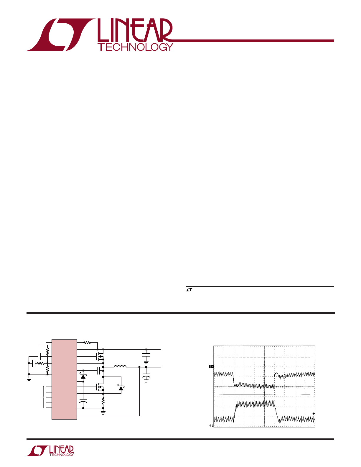
Figure 1. High Efficiency Step-Down Converter
PGND
R
ON
I
ON
V
IN
TG
SW
CB, 0.22µF
D
CMDSH-3
CC
BG
+
B
C
VCC
4.7µF
M1
IRF7811
×2
M2
IRF7811
×3
0.003Ω*
L1
0.68µH
U
D1*
UPS840
+
3714 F01
10µF
35V
×4
C
OUT
270µF
2V
×4
V
IN
5V TO 24V
V
OUT
0.6V TO 1.75V
23A
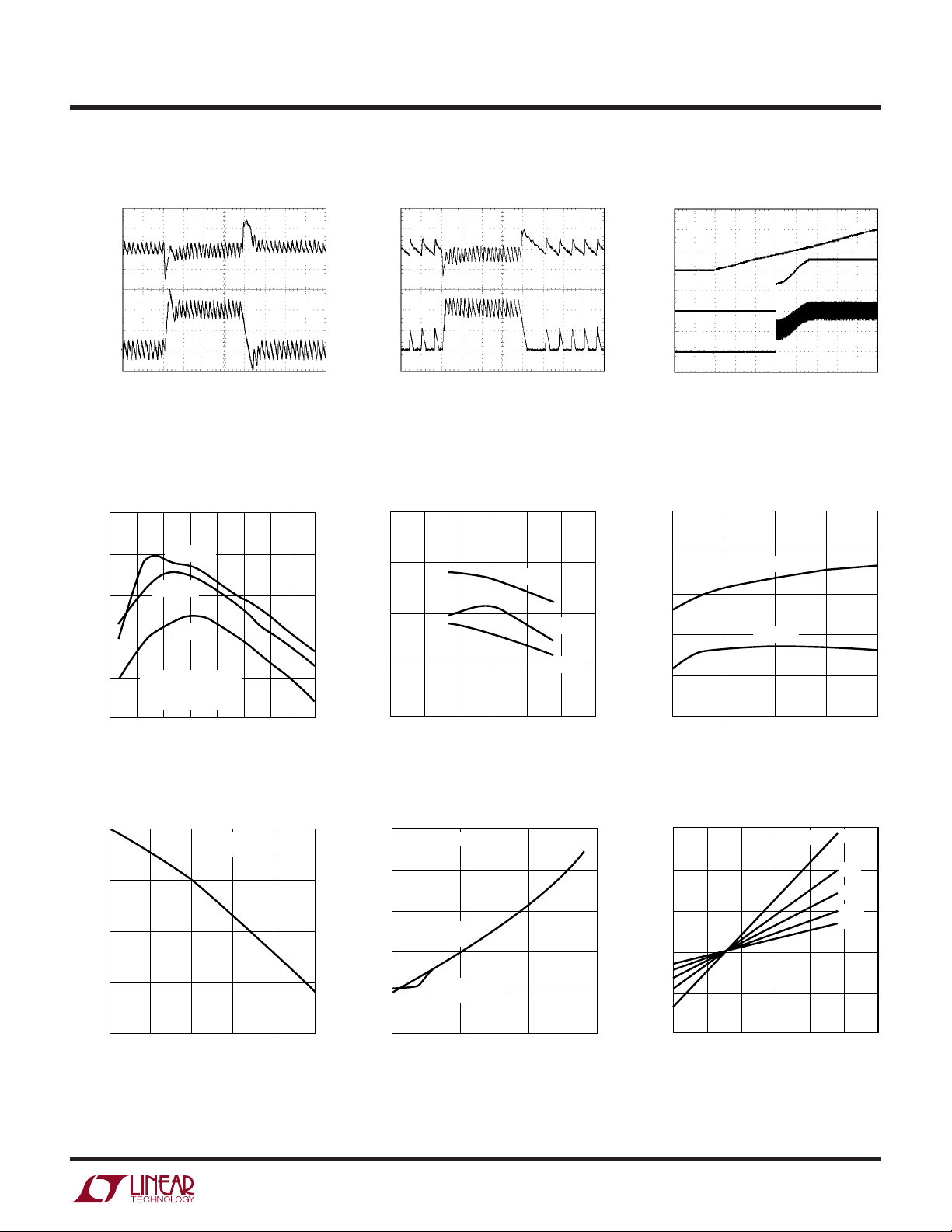
Transient Response of 8A to 23A Output Load Step
1.395V
V
OUT
(1.35V)
50mV/DIV
1.213V
23A
I
LOAD
10A/DIV
8A
20µs/DIV
3714 TA03
3714f
1
LTC3714
WWWU
ABSOLUTE AXI U RATI GS
(Note 1)
Input Supply Voltage (VIN), ION..................36V to –0.3V
Boosted Topside Driver Supply Voltage
(BOOST) ................................................... 42V to –0.3V
SW, SENSE Voltages ................................... 36V to –5V
EXTVCC, (BOOST – SW), RUN/SS, VID0-VID4,
PGOOD, FCB Voltages ............................... 7V to –0.3V
VON, V
ITH, VFB, V
TG, BG, INTVCC, EXTVCC Peak Currents.................... 2A
TG, BG, INTVCC, EXTVCC RMS Currents .............. 50mA
OPVIN, OP+, OP
Operating Ambient Temperature Range
LTC3714EG (Note 2) .......................... –40°C to 85°C
Junction Temperature (Note 3)............................ 125°C
Storage Temperature Range ................. –65°C to 150°C
Lead Temperature (Soldering, 10 sec)..................300°C
Voltages ................(INTVCC + 0.3V) to –0.3V
RNG
Voltages....................... 2.7V to –0.3V
OSENSE
–
.......................................................
0V to 18V
UU
W
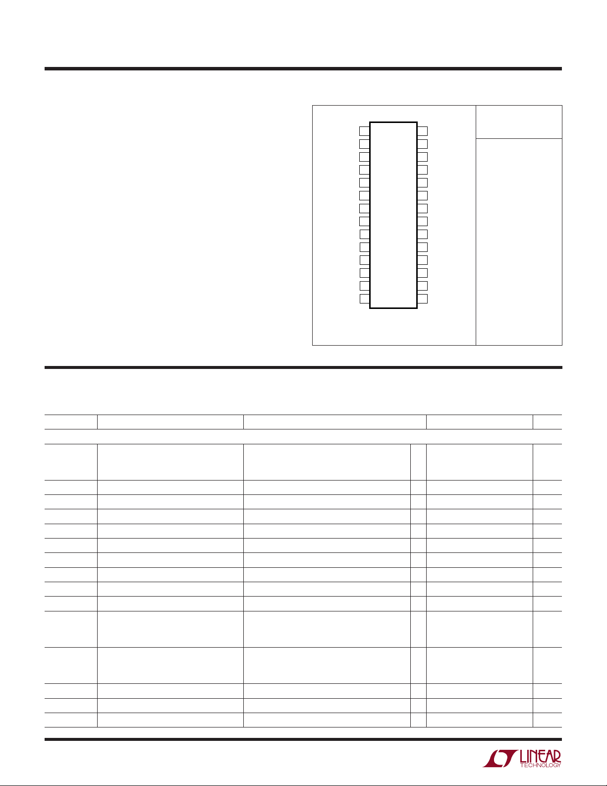
PACKAGE/ORDER I FOR ATIO
TOP VIEW
1
BG
2
PGND
3
SENSE
4
SW
5
TG
6
BOOST
7
VID0
8
VID1
9
VID2
10
RUN/SS
11
V
ON
12
PGOOD
13
V
RNG
14
I
TH
28-LEAD PLASTIC SSOP
T
JMAX
G PACKAGE
= 125°C, θJA = 130°C/W
INTV
28
CC
V
27
IN
EXTV
26
CC
VID4
25
VID3
24
V
23
OSENSE
VFB
22
I
21
ON
FCB
20
SGND
19
OPOUT
18
+
OP
17
–
OP
16
OPV
15
IN
Consult LTC Marketing for parts specified with wider operating temperature ranges.
ORDER PART
NUMBER
LTC3714EG
ELECTRICAL CHARACTERISTICS
The ● denotes specifications which apply over the full operating
temperature range, otherwise specifications are TA = 25°C. VIN = 15V unless otherwise noted.
SYMBOL PARAMETER CONDITIONS MIN TYP MAX UNITS
Main Control Loop
I
Q
V
FB
∆V
FB(LINEREG)
∆V
FB(LOADREG)
g
m(EA)
V
FCB
I
FCB
t
ON
t
ON(MIN)
t
OFF(MIN)
V
SENSE(MAX)
V
SENSE(MIN)
∆V
FB(OV)
∆V
FB(UV)
V
RUN/SS(ON)
Input DC Supply Current
Normal 900 2000 µA
Shutdown Supply Current 15 30 µA
Feedback Reference Voltage ITH = 1.2V (Note 4) ● 0.594 0.600 0.606 V
Feedback Voltage Line Regulation VIN = 4V to 30V (Note 4), ITH = 1.2V 0.002 %/V
Feedback Voltage Load Regulation ITH = 0.5V to 1.9V (Note 4) ● –0.05 –0.3 %
Error Amplifier Transconductance ITH = 1.2V (Note 4) ● 1.4 1.7 2 ms
Forced Continuous Threshold ● 0.57 0.6 0.63 V
Forced Continuous Current V
= 0.6V –1 –2 µA
FCB
On-Time ION = 60µA, VON = 1.5V 200 250 300 ns
Minimum On-Time ION = 180µA, VON = 0V 50 100 ns
Minimum Off-Time ION = 60µA, VON = 1.5V 250 400 ns
Maximum Current Sense Threshold V
Minimum Current Sense Threshold V
= 1V, VFB = 0.56V ● 113 133 153 mV
RNG
= 0V, VFB = 0.56V ● 79 93 107 mV
V
RNG
= INTVCC, VFB = 0.56V ● 158 186 214 mV
V
RNG
= 1V, VFB = 0.64V –67 mV
RNG
V
= 0V, VFB = 0.64V –33 mV
RNG
= INTVCC, VFB = 0.64V –93 mV
V
RNG
Output Overvoltage Fault Threshold 7.5 10 12.5 %
Output Undervoltage Fault Threshold 340 400 460 mV
RUN Pin Start Threshold ● 0.8 1.5 2 V
3714f
2
LTC3714
ELECTRICAL CHARACTERISTICS
The ● denotes specifications which apply over the full operating
temperature range, otherwise specifications are TA = 25°C. VIN = 15V unless otherwise noted.
SYMBOL PARAMETER CONDITIONS MIN TYP MAX UNITS
V
RUN/SS(LE)
V
RUN/SS(LT)
I
RUN/SS(C)
I
RUN/SS(D)
V
IN(UVLO)
V
IN(UVLOR)
TG R
UP
TG R
DOWN
BG R
UP
BG R
DOWN
TG t
r
TG t
f
BG t
r
BG t
f
Internal VCC Regulator
V
INTVCC
∆V
LDO(LOADREG)
V
EXTVCC
∆V
EXTVCC
∆V
EXTVCC(HYS)
PGOOD Output
∆V
FBH
∆V
FBL
∆V
FB(HYS)
V
PGL
VID DAC
V
VID(T)
I
VID(PULLUP)
V
VID(PULLUP)
I
VID(LEAK)
R
VID
∆V
OSENSE
RUN Pin Latchoff Enable Threshold RUN/SS Pin Rising 4 4.5 V
RUN Pin Latchoff Threshold RUN/SS Pin Falling 3.5 4.2 V
Soft-Start Charge Current –0.5 –1.2 –3 µA
Soft-Start Discharge Current 0.8 1.8 3 µA
Undervoltage Lockout Threshold VIN Falling ● 3.4 3.9 V
Undervoltage Lockout Threshold VIN Rising ● 3.5 4 V
TG Driver Pull-Up On Resistance TG High 2 3 Ω
TG Driver Pull-Down On Resistance TG Low 2 3 Ω
BG Driver Pull-Up On Resistance BG High 3 4 Ω
BG Driver Pull-Down On Resistance BG Low 1 2 Ω
TG Rise Time C
TG Fall Time C
BG Rise Time C
BG Fall Time C
Internal VCC Voltage 6V < VIN < 30V, V
Internal VCC Load Regulation ICC = 0mA to 20mA, V
EXTVCC Switchover Voltage ICC = 20mA, V
EXTVCC Switch Drop Voltage ICC = 20mA, V
= 3300pF 20 ns
LOAD
= 3300pF 20 ns
LOAD
= 3300pF 20 ns
LOAD
= 3300pF 20 ns
LOAD
= 4V ● 4.7 5 5.3 V
EXTVCC
= 4V –0.1 ±2%
EXTVCC
Rising ● 4.5 4.7 V
EXTVCC
= 5V 150 300 mV
EXTVCC
EXTVCC Switchover Hysteresis 200 mV
PGOOD Upper Threshold VFB Rising 7.5 10 12.5 %
PGOOD Lower Threshold VFB Falling –7.5 –10 –12.5 %
PGOOD Hysteresis VFB Returning 1 2.5 %
PGOOD Low Voltage I
= 1mA 0.15 0.4 V
PGOOD
VID0-VID4 Logic Threshold Voltage 0.4 1.2 2 V
VID0-VID4 Pull-Up Current V
VID0-VID4 Pull-Up Voltage V
VID0-VID4 Leakage Current V
Resistance from V
OSENSE
to V
FB
DAC Output Accuracy V
to V
VID0
VID0
VID0
= 0V –2.5 µA
VID4
to V
Open 4.5 V
VID4
to V
VID4
= 5V, V
= 0V 0.01 1 µA
RUN/SS
61014 KΩ
Programmed from –0.45 0 0.25 %
OSENSE
0.6V to 1.75V (Note 5)
VIN = 5V unless otherwise noted.
Internal Op Amp
V
OS
I
OS
I
B
Input Offset Voltage 400 1000 µV
Input Offset Current 410 nA
Input Bias Current 45 80 nA
CMRR Common Mode Rejection Ratio VCM = 0V to (VCC – 1V) 100 dB
= 0V to 18V 80 dB
V
CM
3714f
3
LTC3714
ELECTRICAL CHARACTERISTICS
The ● denotes specifications which apply over the full operating
temperature range, otherwise specifications are TA = 25°C. VIN = 5V unless otherwise noted.
SYMBOL PARAMETER CONDITIONS MIN TYP MAX UNITS
PSRR Power Supply Rejection Ratio OPVIN = 3V to 12.5V, OP
A
VOL
V
OL
V
OH
I
SC
I
S
Note 1: Absolute Maximum Ratings are those values beyond which the life
of a device may be impaired.
Note 2: The LTC3714E is guaranteed to meet performance specifications
from 0°C to 70°C. Specifications over the –40°C to 85°C operating
temperature range are assured by design, characterization and correlation
with statistical process controls.
Note 3: T
dissipation P
LTC3714EG: TJ = TA + (PD • 130°C/W)
Large-Signal Voltage Gain OPVIN = 5V, OP
Output Voltage Swing LOW OPVIN = 5V, I
Output Voltage Swing HIGH OPVIN = 5V, I
Short-Circuit Current Short to GND 30 mA
Short to OPV
Supply Current 170 300 µA
is calculated from the ambient temperature TA and power
J
as follows:
D
= 500mV to 4.5V, RL = 10k 1500 V/mV
OUT
= 5mA ● 165 500 mV
SINK
SOURCE
IN
= VO = 1V 100 dB
OUT
= 5mA ● 4.5 4.87 V
40 mA
Note 4: The LTC3714 is tested in a feedback loop that adjusts V
achieve a specified error amplifier output voltage (I
Note 5: The LTC3714 VID DAC is tested in a feedback loop that adjusts
V
to achieve a specified feedback voltage (VFB = 0.6V) for each DAC
OSENSE
VID code.
).
TH
to
FB
4
3714f
UW
TYPICAL PERFOR A CE CHARACTERISTICS
Transient Response
Transient Response
(Discontinuous Mode)
LTC3714
Start-Up
V
OUT
50mV/DIV
I
L
5A/DIV
LOAD STEP 0A TO 10A
V
= 15V
IN
= 1.5V
V
OUT
FCB = 0V
FIGURE 1 CIRCUIT
Efficiency vs Load Current
95
90
85
80
EFFICIENCY (%)
75
70
0
VIN = 8.5V
VIN = 15V
VIN = 24V
V
= 1.35V
OUT
FREQUENCY = 300kHz
FIGURE 1 CIRCUIT
3 6 9 12 15 18 21
LOAD CURRENT (A)
20µs/DIV
3714 G03
3714 G01
V
OUT
50mV/DIV
5A/DIV
I
L
LOAD STEP 1A TO 10A
V
= 15V
IN
= 1.5V
V
OUT
FCB = INTV
FIGURE 1 CIRCUIT
CC
20µs/DIV
3714 G02
RUN/SS
2V/DIV
V
OUT
500mV/DIV
5A/DIV
I
L
VIN = 15V
V
R
OUT
LOAD
= 1.25V
= 0.125Ω
Efficiency vs Input Voltage Frequency vs Input Voltage
100
90
80
EFFICIENCY (%)
70
60
0
I
= 10A
OUT
I
OUT
I
OUT
5101520
INPUT VOLTAGE (V)
= 1A
= 23A
25 30
3714 G04
300
FCB = 0V
FIGURE 1 CIRCUIT
280
260
240
FREQUENCY (kHz)
220
200
5
10
INPUT VOLTAGE (V)
50ms/DIV 3714 G19
I
= 10A
OUT
I
= 0A
OUT
15
20
3714 G05
25
Load Regulation
0
–0.1
(%)
–0.2
OUT
∆V
–0.3
–0.4
0
2
4
LOAD CURRENT (A)
FIGURE 1 CIRCUIT
NO AVP
6
8
3714 G06
Current Sense Threshold
ITH Voltage vs Load Current
2.5
FIGURE 1 CIRCUIT
2.0
1.5
CONTINUOUS
VOLTAGE (V)
1.0
TH
I
0.5
0
10
0
MODE
DISCONTINUOUS
MODE
5
LOAD CURRENT (A)
10
15
3714 G07
vs ITH Voltage
300
200
100
0
–100
CURRENT SENSE THRESHOLD (mV)
–200
0
1.0 1.5 2.0
0.5
ITH VOLTAGE (V)
RNG
=
2V
1.4V
1V
0.7V
0.5V
2.5 3.0
3714 G08
3714f
V
5
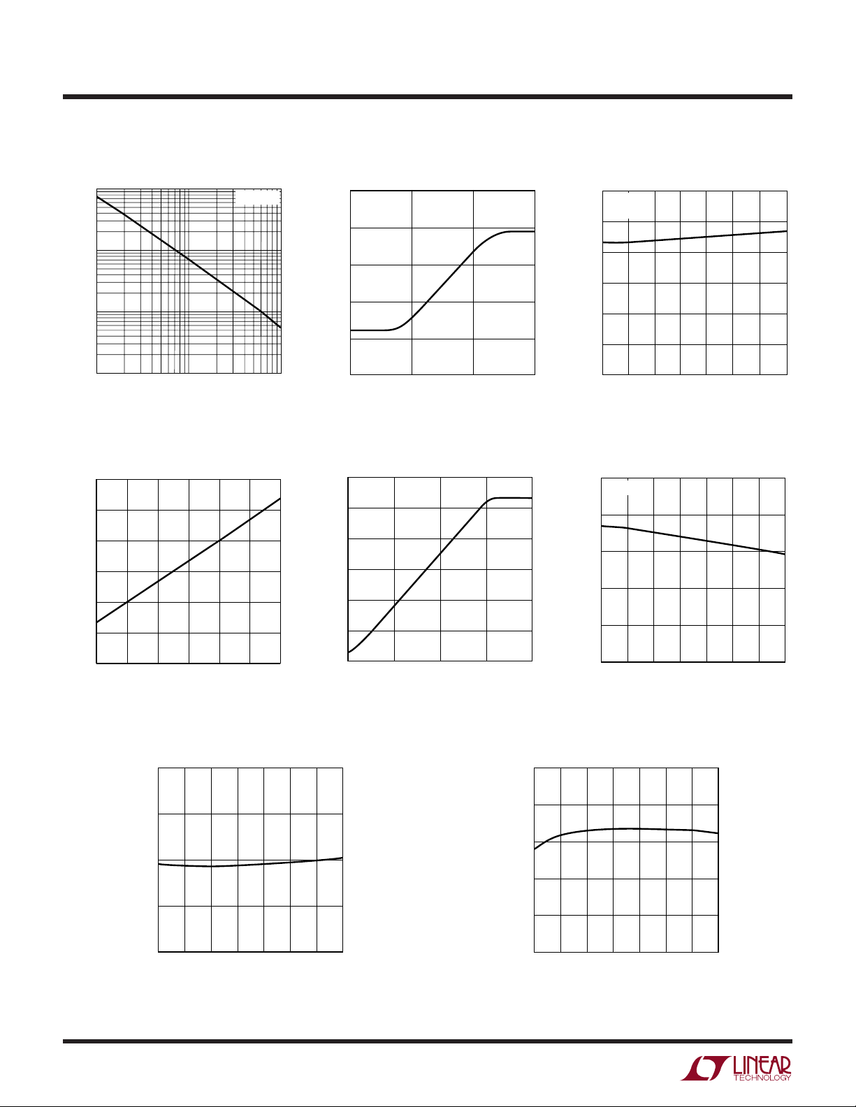
LTC3714
TEMPERATURE (°C)
–50
ON-TIME (ns)
200
250
300
25 75
3714 G22
150
100
–25 0
50 100 125
50
0
I
ION
= 30µA
V
VON
= 0V
UW
TYPICAL PERFOR A CE CHARACTERISTICS
On-Time vs ION Current
10k
1k
ON-TIME (ns)
100
10
1
ION CURRENT (µA)
Maximum Current Sense
Threshold vs V
300
250
200
150
100
50
V
= 0V
VON
10 100
3714 G20
Voltage
RNG
On-Time vs VON Voltage On-Time vs Temperature
1000
I
= 30µA
ION
800
600
400
ON-TIME (ns)
200
0
0
1
VON VOLTAGE (V)
Maximum Current Sense
Threshold vs RUN/SS Voltage
150
125
100
= 1V
V
RNG
75
50
25
2
3
3714 G21
Maximum Current Sense
Threshold vs Temperature
150
V
= 1V
RNG
140
130
120
110
MAXIMUM CURRENT SENSE THRESHOLD (mV)
0
0.5
0.75
1.0 1.25 1.5
V
VOLTAGE (V)
RNG
Feedback Reference Voltage
vs Temperature
0.62
0.61
0.60
6
0.59
FEEDBACK REFERENCE VOLTAGE (V)
0.58
–50
–25 0 25 50
TEMPERATURE (°C)
1.75 2.0
3714 G10
MAXIMUM CURRENT SENSE THRESHOLD (mV)
0
75 100 125
3714 G12
1.5
2 2.5 3 3.5
RUN/SS VOLTAGE (V)
MAXIMUM CURRENT SENSE THRESHOLD (mV)
3714 G23
100
–50 –25
0
TEMPERATURE (°C)
Error Amplifier gm vs Temperature
2.0
1.8
1.6
(mS)
m
g
1.4
1.2
1.0
–50 –25
0
TEMPERATURE (°C)
50
25
50
25
75
100
75
125
3714 G13
100
125
3714 G11
3714f
TEMPERATURE (°C)
–50 –25
0
EXTV
CC
SWITCH RESISTANCE (Ω)
4
10
0
50
75
3714 G14
2
8
6
25
100
125
UW
TYPICAL PERFOR A CE CHARACTERISTICS
LTC3714
Input and Shutdown Currents
vs Input Voltage
1200
1000
INPUT CURRENT (µA)
800
600
400
200
0
0
510
EXTVCC OPEN
SHUTDOWN
EXTVCC = 5V
15 25
INPUT VOLTAGE (V)
FCB Pin Current vs Temperature
0
–0.25
–0.50
–0.75
–1.00
FCB PIN CURRENT (µA)
–1.25
20 30 35
3714 G24
EXTVCC Switch Resistance
INTVCC Load Regulation
–0.1
–0.2
(%)
CC
–0.3
∆INTV
–0.4
–0.5
0
10
0
INTVCC LOAD CURRENT (mA)
30
40
20
50
3714 G25
60
50
SHUTDOWN CURRENT (µA)
40
30
20
10
0
vs Temperature
RUN/SS Pin Current
vs Temperature
3
2
PULL-DOWN CURRENT
1
0
FCB PIN CURRENT (µA)
–1
PULL-UP CURRENT
–1.50
5.0
4.5
4.0
3.5
RUN/SS THRESHOLD (V)
3.0
50 100 125
–50
–25 0
25 75
TEMPERATURE (°C)
RUN/SS Latchoff Thresholds
vs Temperature
LATCHOFF ENABLE
LATCHOFF THRESHOLD
–50
–25 0 25 50
TEMPERATURE (°C)
75 100 125
3714 G15
3714 G17
–2
–50 –25
0
TEMPERATURE (°C)
50
25
75
Undervoltage Lockout Threshold
vs Temperature
4.0
3.5
3.0
2.5
UNDERVOLTAGE LOCKOUT THRESHOLD (V)
2.0
–50
–25 0 25 50
TEMPERATURE (C)
75 100 125
100
125
3714 G16
3714 G18
3714f
7

LTC3714
UUU
PI FU CTIO S
BG (Pin 1): Bottom Gate Drive. Drives the gate of the
bottom N-channel MOSFET between ground and INTVCC.
PGND (Pin 2): Power Ground. Connect this pin closely to
the bottom of the sense resistor or if no sense resistor is
used, to the source of the bottom N-channel MOSFET, the
(–) terminal of C
SENSE (Pin 3): Current Sense Comparator Input. The (+)
input to the current comparator is normally connected to
the SW node unless using a sense resistor (see Applications Information).
SW (Pin 4): Switch Node. The (–) terminal of the bootstrap
capacitor CB connects here. This pin swings from a diode
voltage drop below ground up to VIN.
TG (Pin 5): Top Gate Drive. Drives the top N-channel
MOSFET with a voltage swing equal to INTVCC superimposed on the switch node voltage SW.
BOOST (Pin 6): Boosted Floating Driver Supply. The (+)
terminal of the bootstrap capacitor CB connects here. This
pin swings from a diode voltage drop below INTVCC up to
V
+ INTVCC.
IN
VID0-VID4 (Pins 7, 8, 9, 24, 25): VID Digital Inputs. The
voltage identification (VID) code sets the internal feedback
resistor divider ratio for different output voltages as shown
in Table 1. If unconnected, the pins are pulled high by
internal 2.5µA current sources.
RUN/SS (Pin 10): Run Control and Soft-Start Input. A
capacitor to ground at this pin sets the ramp time to full
output current (approximately 3s/µF) and the time delay
for overcurrent latchoff (see Applications Information).
Forcing this pin below 0.8V shuts down the device.
and the (–) terminal of CIN.
VCC
mum output current and can be set from 0.5V to 2V by a
resistive divider from INTVCC. The sense voltage defaults
to 70mV when this pin is tied to ground, 140mV when tied
to INTVCC.
I
(Pin 14): Current Control Threshold and Error Ampli-
TH
fier Compensation Point. The current comparator threshold increases with this control voltage. The voltage ranges
from 0V to 2.4V with 0.8V corresponding to zero sense
voltage (zero current).
OPVIN (Pin 15): Internal Op Amp Supply. Connect to
INTVCC or a separate supply greater than 5V.
OP– (Pin 16): Negative Input of the Internal Op Amp.
OP+ (Pin 17): Positive Input of the Internal Op Amp.
OPOUT (Pin 18): Output of the Internal Op Amp.
SGND (Pin 19): Signal Ground. All small-signal compo-
nents and compensation components should connect to
this ground, which in turn connects to PGND at one point.
FCB (Pin 20): Forced Continous Input. Tie this pin to
ground to force continuous synchronous operation at low
load, to INTVCC to enable discontinuous mode operation
at low load or to a resistive divider from a secondary output
when using a secondary winding.
ION (Pin 21): On-Time Current Input. Tie a resistor from
VIN to this pin to set the one-shot timer current and thereby
set the switching frequency.
VFB (Pin 22): Error Amplifier Feedback Input. This pin
connects to both the error amplifier input and to the output
of the internal resistive divider. It can be used to attach
additional compensation components if desired.
VON (Pin 11): On-Time Voltage Input. Voltage trip point for
the on-time comparator. Tying this pin to the output
voltage makes the on-time proportional to V
comparator input defaults to 0.7V when the pin is grounded,
2.4V when the pin is tied to INTVCC.
PGOOD (Pin 12): Power Good Output. Open drain logic
output that is pulled to ground when the output voltage is
not within ±10% of the regulation point.
V
(Pin 13): Sense Voltage Range Input. The voltage at
RNG
this pin is ten times the nominal sense voltage at maxi-
OUT
. The
8
V
OSENSE
voltage connects here to the input of the internal resistive
feedback divider.
EXTVCC (Pin 26): External V
ceeds 4.7V, an internal switch connects this pin to INTV
and shuts down the internal regulator so that controller
and gate drive power is drawn from EXTVCC. Do not exceed
7V at this pin and ensure that EXTVCC < VIN.
VIN (Pin 27): Main Input Supply. Decouple this pin to
SGND with an RC filter (1Ω, 0.1µF).
(Pin 23): Output Voltage Sense. The output
Input. When EXTVCC ex-
CC
CC
3714f
UUU
PI FU CTIO S
LTC3714
INTVCC (Pin 28): Internal 5V Regulator Output. The driver
and control circuits are powered from this voltage. De-
U
U
W
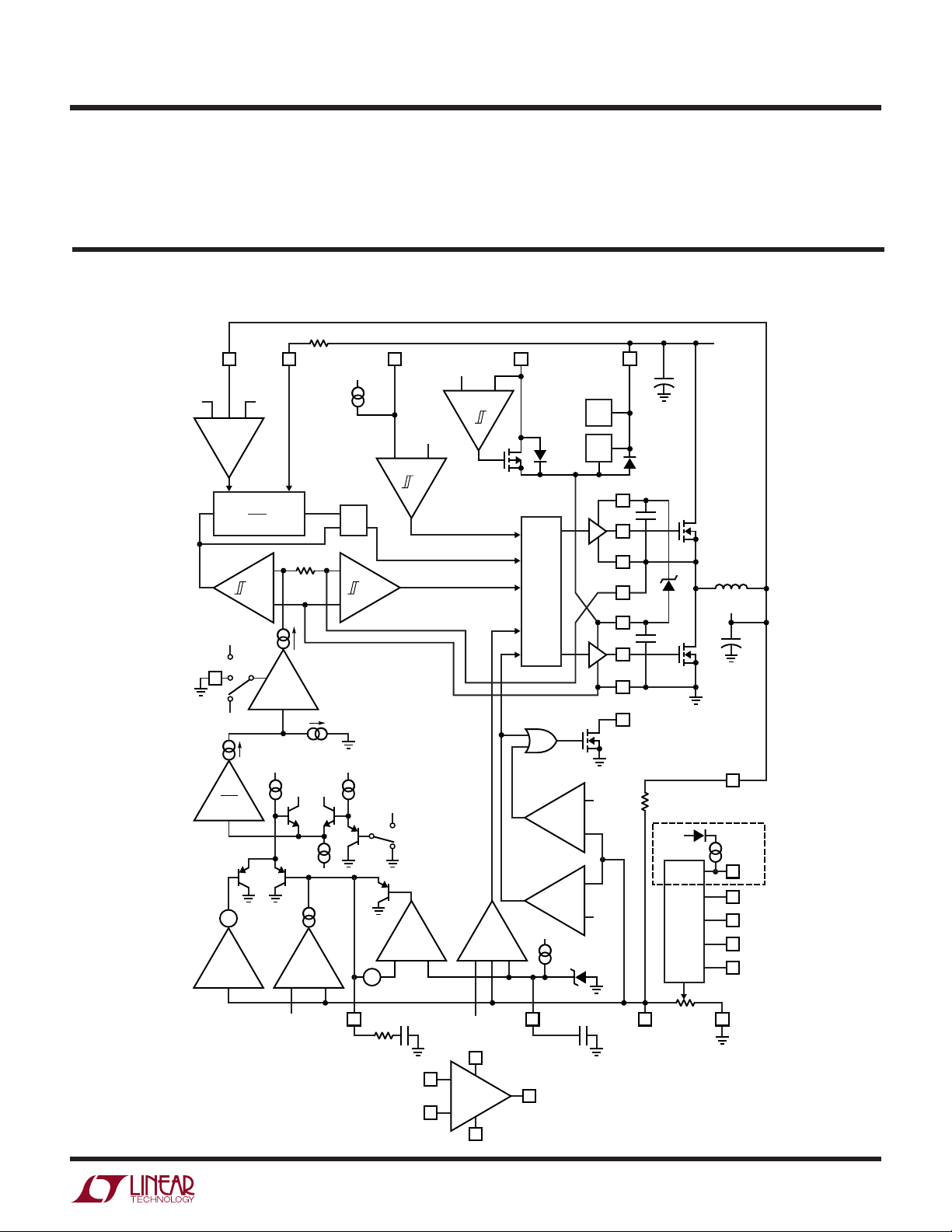
FU CTIO AL DIAGRA
R
ON
0.7V
11
1
tON = (10pF)
1.4V
V
RNG
13
0.7V
V
OST
ON
V
I
I
CMP
VON
ION
2.4V
21
+
–
X
(0.5 TO 2)
I
20k
FCB
1µA
20
4.7V
+
0.6V
+
–
F
ON
R
SQ
+
I
REV
–
couple this pin to power ground with a minimum of 4.7µF
tantalum or other low ESR capacitor.
V
IN
C
IN
M1
L1
V
OUT
+
C
M2
OUT
–
FCNT
SHDN
V
0.6V
REF
REG
27
IN
+
5V
BOOST
6
C
TG
B
5
SW
4
SENSE
3
INTV
CC
28
C
VCC
BG
1
PGND
2
PGOOD
12
EXTV
26
CC
ON
SWITCH
LOGIC
OV
240k
×5.3
3.3µA
V
OSENSE
1
Q4
Q2
Q6
Q3
Q1
+
0.8V
–
EA
–
+
0.6V
1V
Q5
+
OP AMP
–
0.4V
RUN
SHDN
RUN/SS
10
OPV
15
IN
OPOUT
18
SGND
19
SS
–
+
+
–
0.6V
C
C1
I
14
TH
R
C
+
OP
17
–
OP
16
UV
OV
1.2µA
0.54V
+
–
+
0.66V
–
6V
C
SS
R2
10k
5× (ALL VID PINS)
INTV
CC
VID
DAC
R1
22 19
FB
23
2.5µA
7
8
9
24
25
SGNDV
3714 FD
VID0
VID1
VID2
VID3
VID4
3714f
9

LTC3714
OPERATIO
U
Main Control Loop
The LTC3714 is a constant on-time, current mode controller for DC/DC step-down converters. In normal operation,
the top MOSFET is turned on for a fixed interval determined by a one-shot timer OST. When the top MOSFET is
turned off, the bottom MOSFET is turned on until the
current comparator I
timer and initiating the next cycle. Inductor current is
determined by sensing the voltage between the PGND and
SENSE pins using either the bottom MOSFET on-resistance or a separate sense resistor. The voltage on the I
pin sets the comparator threshold corresponding to inductor valley current. The error amplifier EA adjusts this
voltage by comparing the feedback signal VFB from the
output voltage with an internal 0.6V reference. The feedback voltage is derived from the output voltage by a
resistive divider DAC that is set by the VID code pins VID0VID4. If the load current increases, it causes a drop in the
feedback voltage relative to the reference. The ITH voltage
then rises until the average inductor current again matches
the load current.
At low load currents, the inductor current can drop to zero
and become negative. This is detected by current reversal
comparator I
discontinuous operation. Both switches will remain off
with the output capacitor supplying the load current until
the ITH voltage rises above the zero current level (0.8V) to
initiate another cycle. Continuous synchronous operation
can be forced in the LTC3714 by bringing the FCB pin
below 0.6V. The benefit of forced continuous operation is
lower output voltage ripple, faster transient response to
current load steps and a much quieter frequency spectrum
so that it won’t interfere with any neighboring noise
sensitive components.
which then shuts off M2, resulting in
REV
trips, restarting the one-shot
CMP
TH
The operating frequency is determined implicitly by the
top MOSFET on-time and the duty cycle required to
maintain regulation. The one-shot timer generates an ontime that is proportional to the ideal duty cycle, thus
holding frequency approximately constant with changes
in VIN and V
with an external resistor RON.
Overvoltage and undervoltage comparators OV and UV
pull the PGOOD output low if the output feedback voltage
exits a ±10% window around the regulation point. Furthermore, in an overvoltage condition, M1 is turned off and M2
is turned on and held on until the overvoltage condition
clears.
Foldback current limiting is provided if the output is
shorted to ground. As VFB drops, the buffered current
threshold voltage I
level set by Q2 and Q6. This reduces the inductor valley
current level to one sixth of its maximum value as V
approaches ground.
Pulling the RUN/SS pin low forces the controller into its
shutdown state, turning off both M1 and M2. Releasing
the pin allows an internal 1.2µA current source to charge
up an external soft-start capacitor CSS. When this voltage
reaches 1.5V, the controller turns on and begins switching, but with the ITH voltage clamped at approximately
0.6V below the RUN/SS voltage. As CSS continues to
charge, the soft-start current limit is removed.
. The nominal frequency can be adjusted
OUT
is pulled down by clamp Q3 to a 1V
THB
FB
10
3714f

OPERATIO
LTC3714
U
Internal Op Amp
The internal op amp allows the user to program accurate
offsets to the output voltage during power saving modes.
By connecting the OP+ pin to the output, the OPOUT pin to
the V
OSENSE
pin and an external resistor R1 between the
OP–and OPOUT pins, the op amp is hooked up as a unitygain feedback amplifier. Resistors R2 and R3, together
with series switches, can then be placed on the OP– pin to
allow negative offsets to be switched onto the output
voltage (see Figures 2a and 2b). The accuracy of the offset
will depend on the matching of the external resistors R1 to
R2 and R3.*
For applications that require less accurate output offsets,
or none at all, the user can use the internal op amp for true
differential remote sensing of the output voltage by connecting OPOUT to V
OSENSE
and using OP+ and OP– for
differential sensing across the output capacitor as shown
in Figure 2c.
INTVCC/EXTVCC Power
Power for the top and bottom MOSFET drivers and most
of the internal controller circuitry is derived from the
INTVCC pin. The top MOSFET driver is powered from a
floating bootstrap capacitor CB. This capacitor is recharged from INTVCC through an external Schottky diode
DB when the top MOSFET is turned off. When the EXTV
CC
pin is grounded, an internal 5V low dropout regulator
supplies the INTVCC power from VIN. If EXTVCC rises
above 4.7V, the internal regulator is turned off, and an
internal switch connects EXTVCC to INTVCC. This allows
a high efficiency source connected to EXTVCC, such as an
external 5V supply or a secondary output from the
converter, to provide the INTVCC power. Voltages up to
7V can be applied to EXTVCC for additional gate drive. If
the input voltage is low and INTVCC drops below 3.5V,
undervoltage lockout circuitry prevents the power
switches from turning on.
*An alternate configuration, shown in Figure 2b, can be used to program
offsets as well. Either configuration can be used, depending upon the logic
of control signals. If offsets are not required, the op amp can be used to
remotely sense the output voltage, proving true differential sense.
V
V
OUT
OPV
15
+
OP
–
OP
+
17
16
–
SLEEP
MODE
OFFSET
IN
18
R1
BATTERY
MODE
OFFSET
V
OSENSE
23
VID DAC
BATTERY
V
FB
22
R3
3714 F02b
MODE
OFFSET
OPOUT
R2
Figure 2a
+
R
+
V
OUT
V
OUT
R
R
–
OP
–
OP
+
17
16
–
OUT
OPV
15
R1
R2
SLEEP
MODE
OFFSET
+
OP
–
OP
R2
R3
+
17
16
–
IN
18
R1
VID DAC
23
V
FB
22
3714 F02b
Figure 2b
OPV
15
IN
OPOUT V
OSENSE
18R23
3714 F02c
Figure 2c
3714f
11

LTC3714
WUUU
APPLICATIO S I FOR ATIO
The basic LTC3714 application circuit is shown in
Figure 1. External component selection is primarily determined by the maximum load current and begins with
the selection of the sense resistance and power MOSFET
switches. The LTC3714 can use either a sense resistor or
the on-resistance of the synchronous power MOSFET for
determining the inductor current. The desired amount of
ripple current and operating frequency largely determines the inductor value. Finally, CIN is selected for its
ability to handle the large RMS current into the converter
and C
is chosen with low enough ESR to meet the
OUT
output voltage ripple and transient specification.
Maximum Sense Voltage and V
RNG
Pin
Inductor current is determined by measuring the voltage
across a sense resistance that appears between the PGND
and SENSE pins. The maximum sense voltage is set by the
voltage applied to the V
mately (0.133)V
. The current mode control loop will
RNG
pin and is equal to approxi-
RNG
not allow the inductor current valleys to exceed
(0.133)V
RNG/RSENSE
. In practice, one should allow some
margin for variations in the LTC3714 and external component values and a good guide for selecting the sense
resistance is:
V
R
SENSE
=
10 •
RNG
I
()
OUT MAX
An external resistive divider from INTVCC can be used to
set the voltage of the V
pin between 0.5V and 2V
RNG
resulting in nominal sense voltages of 50mV to 200mV.
Additionally, the V
pin can be tied to SGND or INTV
RNG
CC
in which case the nominal sense voltage defaults to 70mV
or 140mV, respectively. The maximum allowed sense
voltage is about 1.33 times this nominal value.
MOSFET as the current sense element by simply connecting the SENSE pin to the switch node SW at the drain of the
bottom MOSFET. This improves efficiency, but one must
carefully choose the MOSFET on-resistance as discussed
below.
Power MOSFET Selection
The LTC3714 requires two external N-channel power
MOSFETs, one for the top (main) switch and one for the
bottom (synchronous) switch. Important parameters for
the power MOSFETs are the breakdown voltage V
threshold voltage V
transfer capacitance C
, on-resistance R
(GS)TH
and maximum current I
RSS
DS(ON)
(BR)DSS
, reverse
DS(MAX)
,
.
The gate drive voltage is set by the 5V INTVCC supply.
Consequently, logic-level threshold MOSFETs must be
used in LTC3714 applications. If the input voltage is
expected to drop below 5V, then sub-logic level threshold
MOSFETs should be considered.
When the bottom MOSFET is used as the current sense
element, particular attention must be paid to its onresistance. MOSFET on-resistance is typically specified
with a maximum value R
DS(ON)(MAX)
at 25°C. In this case,
additional margin is required to accommodate the rise in
MOSFET on-resistance with temperature:
R
R
DS ON MAX
()( )
=
SENSE
ρ
T
The ρT term is a normalization factor (unity at 25°C)
accounting for the significant variation in on-resistance
with temperature, typically about 0.4%/°C as shown in
Figure 3. Junction-to-case temperature is about 30°C in
most applications. For a maximum ambient temperature
of 70°C, using a value ρ
= 1.3 is reasonable.
100°C
Connecting the SENSE Pin
The LTC3714 can be used with or without a sense resistor.
When using a sense resistor, it is placed between the
source of the bottom MOSFET M2 and ground. Connect
the SENSE pin to the source of the bottom MOSFET so that
the resistor appears between the SENSE and PGND pins.
Using a sense resistor provides a well defined current
limit, but adds cost and reduces efficiency. Alternatively,
one can eliminate the sense resistor and use the bottom
12
The power dissipated by the top and bottom MOSFETs
strongly depends upon their respective duty cycles and
the load current. When the LTC3714 is operating in
continuous mode, the duty cycles for the MOSFETs are:
V
D
D
TOP
BOT
OUT
=
V
IN
–
VV
IN OUT
=
V
IN
3714f

WUUU
APPLICATIO S I FOR ATIO
LTC3714
2.0
1.5
1.0
0.5
NORMALIZED ON-RESISTANCE
T
ρ
0
–50
0
JUNCTION TEMPERATURE (°C)
Figure 3. R
50
vs Temperature
DS(ON)
100
150
3714 F02
The resulting power dissipation in the MOSFETs at maximum output current are:
P
TOP
+ k V
P
BOT
= D
TOP IOUT(MAX)
2
I
IN
OUT(MAX) CRSS
= D
BOT IOUT(MAX)
2
ρ
T(TOP) RDS(ON)(MAX)
f
2
ρ
T(BOT) RDS(ON)(MAX)
Tying a resistor RON from VIN to the ION pin yields an ontime inversely proportional to VIN. For a step-down converter, this results in approximately constant frequency
operation as the input supply varies:
V
f
=
VR pF
OUT
VON ON
()10
To hold frequency constant during output voltage changes,
tie the VON pin to V
. The VON pin has internal clamps
OUT
that limit its input to the one-shot timer. If the pin is tied
below 0.7V, the input to the one-shot is clamped at 0.7V.
Similarly, if the pin is tied above 2.4V, the input is clamped
at 2.4V.
Because the voltage at the ION pin is about 0.7V, the
current into this pin is not exactly inversely proportional to
VIN, especially in applications with lower input voltages.
To correct for this error, an additional resistor R
ON2
connected from the ION pin to the 5V INTVCC supply will
further help to stabilize the frequency.
Both MOSFETs have I2R losses and the top MOSFET
includes an additional term for transition losses, which are
largest at high input voltages. The constant k = 1.7A–1 can
be used to estimate the amount of transition loss. The
bottom MOSFET losses are greatest when the bottom duty
cycle is near 100%, during a short-circuit or at high input
voltage.
Operating Frequency
The choice of operating frequency is a tradeoff between
efficiency and component size. Low frequency operation
improves efficiency by reducing MOSFET switching losses
but requires larger inductance and/or capacitance in order
to maintain low output ripple voltage.
The operating frequency of LTC3714 applications is determined implicitly by the one-shot timer that controls the
on-time tON of the top MOSFET switch. The on-time is set
by the current into the ION pin and the voltage at the V
ON
pin according to:
V
t
ON
VON
= ()10
I
ION
pF
V
07=.
5
R
V
R
ON ON2
Changes in the load current magnitude will also cause
frequency shift. Parasitic resistance in the MOSFET
switches and inductor reduce the effective voltage across
the inductance, resulting in increased duty cycle as the
load current increases. By lengthening the on-time slightly
as current increases, constant frequency operation can be
maintained. This is accomplished with a resistive divider
from the ITH pin to the VON pin and V
. The values
OUT
required will depend on the parasitic resistances in the
specific application. A good starting point is to feed about
25% of the voltage change at the ITH pin to the VON pin as
shown in Figure 4a. Place capacitance on the VON pin to
filter out the ITH variations at the switching frequency. The
resistor load on ITH reduces the DC gain of the error amp
and degrades load regulation, which can be avoided by
using the PNP emitter follower of Figure 4b.
3714f
13

LTC3714
14

WUUU
APPLICATIO S I FOR ATIO
LTC3714
The selection of C
is primarily determined by the ESR
OUT
required to minimize voltage ripple and load step
transients. The output ripple ∆V
is approximately
OUT
bounded by:
∆≤∆ +
V I ESR
OUT L
8
fC
1
OUT
Since ∆IL increases with input voltage, the output ripple is
highest at maximum input voltage. Typically, once the ESR
requirement is satisfied, the capacitance is adequate for
filtering and has the necessary RMS current rating.
Multiple capacitors placed in parallel may be needed to
meet the ESR and RMS current handling requirements.
Dry tantalum, special polymer, POSCAP aluminum electrolytic and ceramic capacitors are all available in surface
mount packages. Special polymer capacitors offer very
low ESR but have lower capacitance density than other
types. Tantalum capacitors have the highest capacitance
density but it is important to only use types that have been
surge tested for use in switching power supplies. Aluminum electrolytic capacitors have significantly higher ESR,
but can be used in cost-sensitive applications providing
that consideration is given to ripple current ratings and
long term reliability. Ceramic capacitors have excellent
low ESR characteristics but can have a high voltage
coefficient and audible piezoelectric effects. The high Q of
ceramic capacitors with trace inductance can also lead to
significant ringing. When used as input capacitors, care
must be taken to ensure that ringing from inrush currents
and switching does not pose an overvoltage hazard to the
power switches and controller. High performance throughhole capacitors may also be used, but an additional
ceramic capacitor in parallel is recommended to reduce
the effect of their lead inductance.
Top MOSFET Driver Supply (CB, DB)
An external bootstrap capacitor CB connected to the BOOST
pin supplies the gate drive voltage for the topside MOSFET.
This capacitor is charged through diode DB from INTV
CC
when the switch node is low. When the top MOSFET turns
on, the switch node rises to VIN and the BOOST pin rises
to approximately VIN + INTVCC. The boost capacitor needs
to store about 100 times the gate charge required by the
top MOSFET. In most applications 0.1µF to 0.47µF is
adequate.
Discontinuous Mode Operation and FCB Pin
The FCB pin determines whether the bottom MOSFET
remains on when current reverses in the inductor. Tying
this pin above its 0.6V threshold (typically to INTVCC)
enables discontinuous operation where the bottom
MOSFET turns off when inductor current reverses. The
load current at which current reverses and discontinuous
operation begins, depends on the amplitude of the inductor ripple current. The ripple current depends on the
choice of inductor value and operating frequency as well
as the input and output voltages.
Tying the FCB pin below the 0.6V threshold forces continuous synchronous operation, allowing current to reverse at
light loads.
In addition to providing a logic input to force continuous
operation, the FCB pin provides a means to maintain a
flyback winding output when the primary is operating in
discontinuous mode. The secondary output V
SEC
is normally set as shown in Figure 5 by the turns ratio N of the
transformer. However, if the controller goes into discontinuous mode and halts switching due to a light primary
load current, then V
divider from V
V
SEC(MIN)
until V
SEC
VV
SEC MIN()
OPTIONAL
EXTV
CONNECTION
< 7V
5V < V
SEC
SEC
below which continuous operation is forced
has risen above its minimum.
.=+
06 1
CC
EXTV
R4
FCB
R3
SGND
will droop. An external resistor
SEC
to the FCB pin sets a minimum voltage
R
4
LTC3714
CC
SENSE
V
TG
SW
BG
PGND
R
3
V
IN
+
C
IN
IN
1N4148
V
C
OUT
3714 F05
C
1µF
SEC
SEC
V
OUT
•
T1
1:N
+
•
+
Figure 5. Secondary Output Loop and EXTVCC Connection
15
3714f

LTC3714
WUUU
APPLICATIO S I FOR ATIO
Fault Conditions: Current Limit and Foldback
The maximum inductor current is inherently limited in a
current mode controller by the maximum sense voltage. In
the LTC3714, the maximum sense voltage is controlled by
the voltage on the V
pin. With valley current control,
RNG
the maximum sense voltage and the sense resistance
determine the maximum allowed inductor valley current.
The corresponding output current limit is:
V
SNS MAX
I
=+∆
LIMIT
()
R
* ρ
DS ON T
()
1
I
L
2
The current limit value should be checked to ensure that
I
LIMIT(MIN)
> I
OUT(MAX)
. The minimum value of current limit
generally occurs with the lowest VIN at the highest ambient
temperature. Note that it is important to check for selfconsistency between the assumed junction temperature
and the resulting value of I
which heats the MOSFET
LIMIT
switches.
Caution should be used when setting the current limit
based upon the R
of the MOSFETs. The maximum
DS(ON)
current limit is determined by the minimum MOSFET onresistance. Data sheets typically specify nominal and
maximum values for R
reasonable assumption is that the minimum R
, but not a minimum. A
DS(ON)
DS(ON)
lies
the same amount below the typical value as the maximum
lies above it. Consult the MOSFET manufacturer for further
guidelines.
To further limit current in the event of a short circuit to
ground, the LTC3714 includes foldback current limiting. If
the output falls by more than 50%, then the maximum
sense voltage is progressively lowered to about one sixth
of its full value.
Minimum Off-Time and Dropout Operation
The minimum off-time t
OFF(MIN)
is the smallest amount of
time that the LTC3714 is capable of turning on the bottom
MOSFET, tripping the current comparator and turning the
MOSFET back off. This time is generally about 250ns. The
minimum off-time limit imposes a maximum duty cycle of
tON/(tON + t
OFF(MIN)
). If the maximum duty cycle is reached,
due to a dropping input voltage for example, then the
output will drop out of regulation. The minimum input
voltage to avoid dropout is:
tt
+
VV
IN MIN OUT
=
()
ON OFF MIN
t
ON
()
Output Voltage Programming
The output voltage is digitally set to levels between 0.6V
and 1.75V using the voltage identification (VID) inputs
VID0-VID4. An internal 5-bit DAC configured as a precision resistive voltage divider sets the output voltage in
increments according to Table 1. The VID codes are
compatible with Intel Mobile Pentium® III processor specifications. Each VID input is pulled up by an internal 2.5µA
current source from the INTVCC supply and includes a
series diode to prevent damage from VID inputs that
exceed the supply.
*Use R
value here if a sense resistor is connected between SENSE and PGND.
SENSE
16
3714f

WUUU
APPLICATIO S I FOR ATIO
LTC3714
INTVCC Regulator
An internal P-channel low dropout regulator produces the
5V supply that powers the drivers and internal circuitry
within the LTC3714. The INTVCC pin can supply up to
50mA RMS and must be bypassed to ground with a
minimum of 4.7µF tantalum or other low ESR capacitor.
Good bypassing is necessary to supply the high transient
currents required by the MOSFET gate drivers. Applications using large MOSFETs with a high input voltage and
high frequency of operation may cause the LTC3714 to
exceed its maximum junction temperature rating or RMS
current rating. Most of the supply current drives the
MOSFET gates unless an external EXTVCC source is used.
In continuous mode operation, this current is I
f(Q
g(TOP)
+ Q
). The junction temperature can be
g(BOT)
GATECHG
=
estimated from the equations given in Note 2 of the
Electrical Characteristics. For example, the LTC3714EG is
limited to less than 14mA from a 30V supply:
TJ = 70°C + (14mA)(30V)(130°C/W) = 125°C
For larger currents, consider using an external supply with
the EXTVCC pin.
Table 1. VID Output Voltage Programming
VID4 VID3 VID2 VID1 VID0 V
000001.75V
000011.70V
000101.65V
000111.60V
001001.55V
001011.50V
001101.45V
001111.40V
010001.35V
010011.30V
010101.25V
010111.20V
011001.15V
011011.10V
011101.05V
01111 1.00V
100000.975V
100010.950V
100100.925V
100110.900V
101000.875V
101010.850V
101100.825V
101110.800V
110000.775V
110010.750V
110100.725V
110110.700V
111000.675V
111010.650V
111100.625V
11111 0.600V
OUT
(V)
3714f
17

LTC3714
WUUU
APPLICATIO S I FOR ATIO
EXTVCC Connection
The EXTVCC pin can be used to provide MOSFET gate drive
and control power from the output or another external
source during normal operation. Whenever the EXTV
CC
pin is above 4.7V the internal 5V regulator is shut off and
an internal 50mA P-channel switch connects the EXTV
CC
pin to INTVCC. INTVCC power is supplied from EXTVCC until
this pin drops below 4.5V. Do not apply more than 7V to
the EXTVCC pin and ensure that EXTVCC ≤ VIN. The following list summarizes the possible connections for EXTVCC:
1. EXTVCC grounded. INTV
is always powered from the
CC
internal 5V regulator.
2. EXTVCC connected to an external supply. A high efficiency supply compatible with the MOSFET gate drive
requirements (typically 5V) can improve overall
efficiency.
3. EXTVCC connected to an output derived boost network.
The low voltage output can be boosted using a charge
pump or flyback winding to greater than 4.7V. The system
will start-up using the internal linear regulator until the
boosted output supply is available.
External Gate Drive Buffers
The LTC3714 drivers are adequate for driving up to about
60nC into MOSFET switches with RMS currents of 50mA.
Applications with larger MOSFET switches or operating at
frequencies requiring greater RMS currents will benefit
from using external gate drive buffers such as the LTC1693.
Alternately, the external buffer circuit shown in Figure 6
can be used. Note that the bipolar devices reduce the
signal swing at the MOSFET gate, and benefit from increased EXTVCC voltage of about 6V.
10Ω
INTV
PGND
CC
Q3
FMMT619
Q4
FMMT720
GATE
OF M2
3714 F06
BOOST
Q1
FMMT619
10Ω
TG
Q2
FMMT720
SW
Figure 6. Optional External Gate Driver
GATE
OF M1
BG
18
3714f

WUUU
APPLICATIO S I FOR ATIO
LTC3714
Soft-Start and Latchoff with the RUN/SS Pin
The RUN/SS pin provides a means to shut down the
LTC3714 as well as a timer for soft-start and overcurrent
latchoff. Pulling the RUN/SS pin below 1.5V puts the
LTC3714 into a low quiescent current shutdown (IQ ≤
30µA). Releasing the pin allows an internal 1.2µA internal
current source to charge up the external timing capacitor
CSS. If RUN/SS has been pulled all the way to ground, there
is a delay before starting of about:
15
.
t
DELAY SS SS
V
=
12
CsFC
.
A
µ
13
./
=µ
()
When the voltage on RUN/SS reaches 1.5V, the LTC3714
begins operating with a clamp on ITH of approximately
0.9V. As the RUN/SS voltage rises to 3V, the clamp on I
TH
is raised until its full 2.4V range is available. This takes an
additional 1.3s/µF, during which the load current is folded
back until the output reaches 50% of its final value. The pin
can be driven from logic as shown in Figure 7. Diode D1
reduces the start delay while allowing CSS to charge up
slowly for the soft-start function.
After the controller has been started and given adequate
time to charge up the output capacitor, CSS is used as a
short-circuit timer. After the RUN/SS pin charges above
4V, if the output voltage falls below 75% of its regulated
value, then a short-circuit fault is assumed. A 1.7µA cur-
rent then begins discharging CSS. If the fault condition
persists until the RUN/SS pin drops to 3.5V, then the con-
troller turns off both power MOSFETs, shutting down the
converter permanently. The RUN/SS pin must be actively
pulled down to ground in order to restart operation.
The overcurrent protection timer requires that the softstart timing capacitor CSS be made large enough to guarantee that the output is in regulation by the time CSS has
reached the 4V threshold. In general, this will depend upon
the size of the output capacitance, output voltage and load
current characteristic. A minimum soft-start capacitor can
be estimated from:
CSS > C
OUT VOUT RSENSE
(10–4 [F/Vs])
Generally 0.1µF is more than sufficient.
Overcurrent latchoff operation is not always needed or
desired. Load current is already limited during a shortcircuit by the current foldback circuitry and latchoff
operation can prove annoying during troubleshooting.
The feature can be overridden by adding a pull-up current
of >5µA to the RUN/SS pin. The additional current prevents the discharge of CSS during a fault and also shortens
the soft-start period. Using a resistor to VIN as shown in
Figure 7a is simple, but slightly increases shutdown
current. Connecting a resistor to INTVCC as shown in
Figure 7b eliminates the additional shutdown current, but
requires a diode to isolate CSS. Any pull-up network must
be able to pull RUN/SS above the 4.5V maximum threshold that arms the latchoff circuit and overcome the 4µA
maximum discharge current.
INTV
CC
V
3.3V OR 5V RUN/SS
Figure 7. RUN/SS Pin Interfacing with Latchoff Defeated
IN
RSS*
D1
C
SS
*OPTIONAL TO OVERRIDE
OVERCURRENT LATCHOFF
(7a) (7b)
RSS*
D2*
RUN/SS
C
SS
3714 F07
3714f
19

LTC3714
WUUU
APPLICATIO S I FOR ATIO
Efficiency Considerations
The percent efficiency of a switching regulator is equal to
the output power divided by the input power times 100%.
It is often useful to analyze individual losses to determine
what is limiting the efficiency and which change would
produce the most improvement. Although all dissipative
elements in the circuit produce losses, four main sources
account for most of the losses in LTC3714 circuits:
1. DC I2R losses. These arise from the resistances of the
MOSFETs, inductor and PC board traces and cause the
efficiency to drop at high output currents. In continuous
mode the average output current flows through L, but is
chopped between the top and bottom MOSFETs. If the two
MOSFETs have approximately the same R
resistance of one MOSFET can simply be summed with the
resistances of L and the board traces to obtain the DC I2R
loss. For example, if R
loss will range from 15mW up to 1.5W as the output
current varies from 1A to 10A for a 1.5V output.
2. Transition loss. This loss arises from the brief amount
of time the top MOSFET spends in the saturated region
during switch node transitions. It depends upon the input
voltage, load current, driver strength and MOSFET capacitance, among other factors. The loss is significant at input
voltages above 20V and can be estimated from:
Transition Loss ≅ (1.7A–1) V
3. INTVCC current. This is the sum of the MOSFET driver
and control currents. This loss can be reduced by supplying INTVCC current through the EXTVCC pin from a high
efficiency source, such as an output derived boost network or alternate supply if available.
4. CIN loss. The input capacitor has the difficult job of
filtering the large RMS input current to the regulator. It
must have a very low ESR to minimize the AC I2R loss and
sufficient capacitance to prevent the RMS current from
causing additional upstream losses in fuses or batteries.
Other losses, including C
conduction loss during dead time and inductor core loss
generally account for less than 2% additional loss.
= 0.01Ω and RL = 0.005Ω, the
DS(ON)
2
I
IN
OUT CRSS
ESR loss, Schottky diode D1
OUT
DS(ON)
f
, then the
When making any adjustments to improve efficiency, the
final arbiter is the total input current for the regulator at
your operating point. If you make a change and the input
current decreases, then you improved the efficiency. If
there is no change in input current, then there is no change
in efficiency.
Checking Transient Response
The regulator loop response can be checked by looking at
the load transient response. Switching regulators take
several cycles to respond to a step in load current. When
a load step occurs, V
equal to ∆I
resistance of C
discharge C
the regulator to return V
During this recovery time, V
overshoot or ringing that would indicate a stability problem. The ITH pin external components shown in Figure 8
will provide adequate compensation for most applications. For a detailed explanation of switching control loop
theory see Linear Technology Application Note 76.
Design Example
As a design example, take a supply with the following
specifications: VIN = 7V to 24V (15V nominal),
V
= 1.15V ±100mV, I
OUT
calculate the timing resistor with VON = V
R
=
ON
and choose the inductor for about 40% ripple current at
the maximum VIN:
L
300 0 4 15
()()()
Choosing a standard value of 0.68µH results in a maxi-
mum ripple current of:
∆=
L
(ESR), where ESR is the effective series
LOAD
OUT
generating a feedback error signal used by
OUT
kHz pF
300 10
()()
115
.
kHz A
115
kHz H
300 0 68
()
immediately shifts by an amount
OUT
. ∆I
1
V
.
V
.
.
()
also begins to charge or
LOAD
to its steady-state value.
OUT
can be monitored for
OUT
OUT(MAX)
µ
= 15A, f = 300kHz. First,
OUT
k
=
330
V
115
.
−
1
1
–
V
24
115
.
24
=µ
06
V
=I
V
:
.
54
.
H=
A
20
3714f

WUUU
P
VVVA
W
BOT
=
()
Ω
()
=
24 1 152420
2
16 0013 198
2
–.
.. .
APPLICATIO S I FOR ATIO
LTC3714
Next, choose the synchronous MOSFET switch. Because
of the narrow duty cycle and large current, a single SO-8
MOSFET will have difficulty dissipating the power lost in
the switch. Choosing two IRF7811s (R
C
= 60pF) yields a nominal sense voltage of:
RSS
V
SNS(NOM)
Tying V
= (15A)(0.5)(1.3)(0.013Ω) = 127mV
to INTVCC will set the current sense voltage
RNG
DS(ON)
= 0.013Ω,
range for a nominal value of 140mV with current limit
occurring at 186mV. To check if the current limit is
acceptable, assume a junction temperature of about 100°C
above a 50°C ambient with ρ
C
SS
0.1µF
R
100k
C
C1
R
2.2nF
C
20k
C
C2
100pF
C
0.01µF
ION
C
100pF
FB
R
ON
330k
150°C
PG
9
10
11
12
13
14
19
21
22
20
23
24
15
16
= 1.6:
VID2
RUN/SS
V
ON
PGOOD
V
RNG
I
TH
LTC3714
SGND
I
ON
V
FB
FCB
V
OSENSE
VID3
OPV
IN
–
OP
VID1
VID0
BOOST
SW
SENSE
PGND
INTV
EXTV
VID4
OPOUT
OP
8
7
C
B
0.33µF
C
VCC
4.7µF
CMDSH-3
C
0.1µF
6
5
TG
4
3
2
1
BG
28
CC
27
V
IN
26
5V
CC
25
18
17
+
I
LIMIT
≥
186
05 16 0013
...
()()
()
Ω
1
+
AA
=
54 20
.
()
2
mV
and double check the assumed TJ in the MOSFET:
TJ = 50°C + (1.98W)(50°C/W) = 149°C
D
B
V
IN
7V TO 24V
C
IN
M1
IRF7811
M2
IRF7811
×2
R
F
1Ω
F
L1
0.68µH
D1
UPS840
22µF
25V
×3
C
OUT
270µF
2V
×5
V
OUT
1.15V
15A
: UNITED CHEMICON THCR70EIH226ZT
C
IN
: PANASONIC EEFUE0D271
C
OUT
L1: SUMIDA CEP125-4712-T007
Figure 8. CPU Core Voltage Regulator 1.15V/15A at 300kHz without Active Voltage Positioning
3714 F08
3714f
21

LTC3714
WUUU
APPLICATIO S I FOR ATIO
Because the top MOSFET is on for such a short time, a
single IRF7811 will be sufficient. Checking its power
dissipation at current limit with ρ
.
115
P
=
TOP
()( )( )( )( )
TJ = 50°C + (0.652W)(50°C/W) = 82.6°C
The junction temperatures will be significantly less at
nominal current, but this analysis shows that careful
attention to heat sinking will be necessary in this circuit.
CIN is chosen for an RMS current rating of about 6A at
temperature. The output capacitors are chosen for a low
ESR of 0.005Ω to minimize output voltage changes due to
inductor ripple current and load steps. The ripple voltage
will be only:
∆V
OUT(RIPPLE)
= 27mV
However, a 0A to 15A load step will cause an output
change of up to:
∆V
OUT(STEP)
The complete circuit is shown in Figure 8.
V
24
V
.
1 7 24 20 60 300
...
=+=
0 299 0 353 0 652
= ∆I
2
20 1 2 0 013
()()
2
V A pF kHz
WWW
= ∆I
LOAD
..
A
L(MAX)
()
(ESR) = (5.4A) (0.005Ω)
(ESR) = (15A) (0.005Ω) = ±75mV
80°C
= 1.2:
Ω
+
1
∆=
OUT STEP()
By positioning the output voltage 60mV above the regulation point at no load, it will drop 65mV below the regulation
point after the load step. However, when the load disappears or the output is stepped from 15A to 0A, the 65mV
is recovered. This way, a total of 65mV change is observed
on V
150mV is seen on V
Implementing active voltage positioning requires setting a
precise gain between the sensed current and the output
voltage. Because of the variability of MOSFET on-resistance, it is prudent to use a sense resistor with active
voltage positioning. In order to minimize power lost in this
resistor, a low value of 0.003Ω is chosen. The nominal
sense voltage will now be:
To maintain a reasonable current limit, the voltage on the
V
INTVCC and GND, corresponding to a 50mV nominal sense
voltage.
Next, the gain of the LTC3714 error amplifier must be
determined. The change in ITH voltage for a corresponding
change in the output current is:
in all conditions, whereas a total of ±75mV or
OUT
V
SNS(NOM)
pin is reduced to 0.5V by connecting it between
RNG
()
OUT
= (0.003Ω)(15A) = 45mV
()
3
without voltage positioning.
Ω
.15
0 025 125
=VA mV
Active Voltage Positioning
Active voltage positioning (also termed load “deregulation” or droop) describes a technique where the output
voltage varies with load in a controlled manner. It is useful
in applications where rapid load steps are the main cause
of error in the output voltage. By positioning the output
voltage at or above the regulation point at zero load, and
below the regulation point at full load, one can use more
of the error budget for the load step. This allows one to
reduce the number of output capacitors by relaxing the
ESR requirement.
In the design example, Figure 8, five 0.025Ω capacitors
are required in parallel to keep the output voltage within
tolerance. Using active voltage positioning, the same
specification can be met with only three capacitors. In this
case, the load step will cause an output voltage change of:
22
∆=
The corresponding change in the output voltage is determined by the gain of the error amplifier and feedback
divider. The LTC3714 error amplifier has a
transconductance gm that is constant over both temperature and a wide ± 40mV input range. Thus, by connecting
a load resistance RVP to the ITH pin, the error amplifier gain
can be precisely set for accurate voltage positioning.
∆=
I
TH
=
()
TH m VP
12
V
RI
V
RNG
24 0 003 15 1 08..
()()
06.
V
∆
SENSE OUT
Ω
AV
V
∆IgR
V
OUT
OUT
=
3714f

WUUU
APPLICATIO S I FOR ATIO
LTC3714
Solving for this resistance value:
VI
∆
R
VP
==
OUT TH
=
Vg V
(. )
06
(. )(. )( )
06 17 60
∆
m OUT
VV
(. )(. )
115 108
VmSmV
.
20 3
k
The gain setting resistance RVP is implemented with two
resistors, R
connected from ITH to ground and R
VP1
VP2
connected from ITH to INTVCC. The parallel combination of
these resistors must equal RVP and their ratio determines
0.1µF
R
RNG1
10k
2.2nF
C
9
C
SS
R
RNG2
90.1k
C
C1
R
C
20k
0.01µF
ION
R
ON
330k
R
VP2
185k
R
VP1
23k
C
INTV
100pF
FB
CC
0.1µF
R
PG
100k
C
100pF
VID2
10
RUN/SS
11
V
ON
12
PGOOD
13
V
RNG
LTC3714
14
I
TH
C1
19
SGND
21
I
ON
22
V
FB
20
FCB
23
V
OSENSE
24
VID3
15
OPV
IN
16
–
OP
VID1
VID0
BOOST
SENSE
PGND
INTV
EXTV
VID4
OPOUT
OP
SW
BG
V
8
7
6
5
TG
4
3
2
1
28
CC
27
IN
26
5V
CC
25
18
17
+
nominal value of the ITH pin voltage when the error
amplifier input is zero. To set the beginning of the load line
at the regulation point, the ITH pin voltage must be set to
correspond to zero output current. The relation between
voltage and the output current is:
C
B
0.33µF
C
VCC
4.7µF
I
TH NOM
D
B
CMDSH-3
R
1Ω
C
F
0.1µF
=
=
055
=
F
12 1
V
RI I V
V
RNG
12
V
0 003 0
()
05
V
.
V
.
M1
IRF7811
0.68µH
M2
IRF7811
×2
R
SENSE
0.003Ω
SENSE OUT L()
AA V
Ω
.–..
L1
D1
UPS840
–.
∆
2
1
54 075
2
C
IN
10µF
25V
×3
C
OUT
270µF
2V
×3
075
+
+
V
IN
7V TO 24V
V
OUT
1.15V/15A
C
: UNITED CHEMICON THCR70EIH226ZT
IN
: PANASONIC EEFUE0D271
C
OUT
L1: SUMIDA CEP125-4712-T007
Figure 9. CPU Core Voltage Regulator with Active Voltage Positioning 1.15V/15A at 300kHz
3714 F08
3714f
23

LTC3714
WUUU
APPLICATIO S I FOR ATIO
Solving for the required values of the resistors:
V
R
==
VP
1
=
R
===
VP
2
5
VI
5
––.
TH NOM
k
23
V
55
I
TH NOM
()
R
()
R
VP
VP
055
.
V
+
V
C
IN
IN
–
–
C
V
OUT
OUT
+
V
5
VV
5055
20 3 185
.
20 3
kk
V
M1
M2
D1
.
The modified circuit is shown in Figure 9. Refer to Linear
Technology Design Solutions 10 for additional information about output voltage positioning.
k
PC Board Layout Checklist
When laying out the printed circuit board, use the following checklist to ensure proper operation of the controller.
C
VCC
LTC3714
1
BG
PGND
2
3
SENSE
D
B
4
SW
INTV
EXTV
V
VID4
28
CC
27
IN
26
CC
25
C
F
R
F
R
ON
C
C
BOLD LINES INDICATE HIGH CURRENT PATHS
Figure 10. LTC3714 Layout Diagram
V
OSENSE
SGND
OPOUT
OPV
VID3
V
I
FCB
OP
OP
24
23
22
FB
21
ON
20
19
18
17
+
16
–
15
IN
C
ION
C
3714 F10
FB
5
10
11
12
13
14
6
7
8
9
C
TG
BOOST
VID0
VID1
VID2
RUN/SS
V
ON
PGOOD
V
RNG
I
TH
C2
C
B
SS
C1
R
C
24
3714f

WUUU
APPLICATIO S I FOR ATIO
LTC3714
These items are also illustrated in Figures 10 and 11.
• Segregate the signal and power grounds. All small
signal components should return to the SGND pin at
one point which is then tied to the PGND pin close to the
source of M2.
• Place M2 as close to the controller as possible, keeping
the PGND, BG and SENSE traces short.
•
Connect the input capacitor(s) CIN close to the power
MOSFETs. This capacitor carries the MOSFET AC
current.
V
IN
C
IN
C
IN
C
IN
C
IN
SW
• Keep the high dV/dT SW, BOOST and TG nodes away
from sensitive small-signal nodes.
• Connect the INTVCC decoupling capacitor C
VCC
closely
to the INTVCC and PGND pins.
• Connect the top driver boost capacitor CB closely to the
BOOST and SW pins.
• Connect the VIN pin decoupling capacitor CF closely to
the VIN and PGND pins.
• VID0-VID4 interface circuitry must return to SGND.
TO PGND
(PIN 2)
R
SENSE
PGND
M1 M2
C
OUT
SENSE
PGND
C
OUTCOUTCOUT
V
OUT
M1
D1
M2
M2
L1
Figure 11. General Layout of External Power Components
TO SENSE
(PIN 3)
3714 F11
3714f
25

LTC3714
TYPICAL APPLICATIO
Performance Data for Intel Compatible Mobile Microprocessor Power Supply with Active Voltage Positioning
U
Line Transient Reponse from VIN = 9V to 17V Load Transient Reponse for I
V
IN
5V/DIV
V
OUT
50mV/DIV
AC COUPLED
50µs/DIV
3714 TA02
20µs/DIV
Efficiency
95
V
= 1.35V
OUT
90
85
80
EFFICIENCY (%)
VIN = 8.5V
VIN = 15V
VIN = 24V
= 8A to 23A
OUT
3714 TA03
1.395V
V
OUT
(1.35V)
50mV/DIV
1.213V
23A
I
LOAD
10A/DIV
8A
26
75
70
0 3 6 9 12 15 18 21
LOAD CURRENT (A)
3714 TA04
3714f

TYPICAL APPLICATIO
Transmeta CrusoeTM Microprocessor Power Supply with Active Voltage Positioning
3.3V
VRON
V
R22
100k
1k
3.3V
IN
V
OUT
V
IN
POWER GOOD
2k
DPSLP
BAT54C
START
1µF
100Ω
10k
0.1µF
220pF
0.1µF
U
INTV
0.01µF
820pF
13k 1%
1000pF
100pF
1M
1k
CC
3.2k
20k
10k
80.6k 1%
330k
200k
BAT54
BAT54
VID3
200k
START
VID2
U1 LTC3714EG
9
VID2
10
RUN/SS
11
V
ON
12
PGOOD
13
V
RNG
LTC3714EG
14
I
TH
19
SGND
20
FCB
21
I
ON
22
V
FB
23
V
OSENSE
24
VID3
18
OPOUT
15
OPV
IN
0.01µF
100k
1%
DPSLP
BOOST
SENSE
PGND
INTV
EXTV
VID1
VID0
SW
VID4
OP
OP
TG
BG
CC
V
IN
CC
+
–
VID1 VID0 3.3V
CMDSH-3
5V
0.22µF
1Ω
453k
1%
75k
1%
200k
200k
4.7µF
0.1µF
200k
8
7
6
5
4
3
2
1
28
27
25
26
17
16
LTC3714
V
IN
C
IN
IRF7811
L1
1.8µH
IRF7811
0.005Ω
V
IN
3.3V
VID4
V
OUT
MBRS340
10µF
35V
×2
+
C
OUT
270µF
2V
×2
5V TO 24V
V
OUT
0.6V To 1.75V
8A
1µF
6.3V
3714 TA01
PACKAGE DESCRIPTIO
5.20 – 5.38**
(.205 – .212)
° – 8°
0
.13 – .22
(.005 – .009)
NOTE:
1. CONTROLLING DIMENSION: MILLIMETERS
2. DIMENSIONS ARE IN
3. DRAWING NOT TO SCALE
*
DIMENSIONS DO NOT INCLUDE MOLD FLASH. MOLD FLASH
SHALL NOT EXCEED .152mm (.006") PER SIDE
**
DIMENSIONS DO NOT INCLUDE INTERLEAD FLASH. INTERLEAD
FLASH SHALL NOT EXCEED .254mm (.010") PER SIDE
.55 – .95
(.022 – .037)
MILLIMETERS
(INCHES)
Information furnished by Linear Technology Corporation is believed to be accurate and reliable.
However, no responsibility is assumed for its use. Linear Technology Corporation makes no representation that the interconnection of its circuits as described herein will not infringe on existing patent rights.
.65
(.0256)
BSC
U
G Package
28-Lead Plastic SSOP (5.3mm)
(Reference LTC DWG # 05-08-1640)
.25 – .38
(.010 – .015)
Crusoe is a trademark of Transmeta Corporation.
1.73 – 1.99
(.068 – .078)
.05 – .21
(.002 – .008)
10.07 – 10.33*
(.397 – .407)
2526 22 21 20 19 181716 1523242728
12345678 9 10 11 12 1413
7.65 – 7.90
(.301 – .311)
G28 SSOP 0501
3714f
27

LTC3714
TYPICAL APPLICATIO
Intel Compatible Mobile Microprocessor Power Supply with Active Voltage Positioning
INTV
U
3.3V
CC
V
RON
POWER GOOD
3.2k
220pF
20.5k
1%
200k
0.1µF
1k
220pF
100pF
1k
200k
0.1µF
10nF
20k
10
11
12
13
14
19
21
22
20
23
24
18
15
9
VID2
RUN/SS
V
ON
PGOOD
V
RNG
I
TH
SGND
I
ON
V
FB
FCB
V
OSENSE
VID3
OPOUT
OPV
IN
VID1
VID0
BOOST
TG
SW
SENSE
LTC3714
PGND
BG
INTV
V
VID4
EXTV
OP
OP
330k
200k
8
200k
7
6
0.22µF
5
4
CMDSH-3
3
2
1
28
CC
IN
CC
+
–
+
4.7µF
0.1µF
10k
1%
10V
200k
3.3V
5V
GMUXSEL
1Ω
27
25
26
17
16
7V ≤ V
IN
≤ 24V
IRF7811
×2
IRF7811
×3
R
SENSE
0.003Ω
806k
1%
L1
0.68µH
MBRS
340T3
10k
1%
+
C
IN
10µF
35V
×4
V
OUT
0.6V TO 1.75V
23A
C
OUT
270µF
2V
×4
3.3V
100Ω
2k
10k
INTV
INTV
3.3V
1µF
200k
1%
CC
CC
INTV
CC
277k
1%
DPRSLPVR
3714 TA01
DPSLP#
806k
1%
100Ω
10k
RELATED PARTS
PART NUMBER DESCRIPTION COMMENTS
LTC1778 Low Duty Cycle, No R
LTC3711 5-Bit Adjustable, Low Duty Cycle, No R
Step-Down Controller 0.925V ≤ V
LTC3716 Dual Phase, High Efficiency Step-Down Controller 2-Phase, 5-Bit VID (0.6V to 1.75V), Narrow 36-Pin SSOP, 3.5V ≤ VIN ≤ 36V
LTC3778 Wide VIN, No R
No R
is a trademark of Linear Technology Corporation.
SENSE
SENSE
Linear Technology Corporation
28
1630 McCarthy Blvd., Milpitas, CA 95035-7417
(408) 432-1900 ● FAX: (408) 434-0507
TM
Step-Down Controller GN-16 Package, 0.8V Reference, Burst Mode Operation
SENSE
, GN-24 Package, 5-Bit VID, 0.8V
SENSE
OUT
≤ 2V
, Burst Mode Operation,
REF
Step-Down Controller 4V ≤ VIN ≤ 36V, True Current Mode Control, 1A ≤ I
●
www.linear.com
LINEAR TECHNOLOGY CORPORATION 2001
≤ 20A
OUT
3714f
LT/TP 0602 2K • PRINTED IN USA
 Loading...