

查询LTC3711EGN供应商
FEATURES
LTC3713
Low Input Voltage,
High Power, No R
SENSE
TM
Synchronous Buck DC/DC Controller
U
DESCRIPTIO
■
Very Low V
■
True Current Mode Control
■
5V Drive for N-Channel MOSFETs Eliminates
IN(MIN)
: 1.5V
Auxillary 5V Supply
■
No Sense Resistor Required
■
Uses Standard 5V Logic-Level N-Channel MOSFETs
■
Adjustable Current Limit
■
Adjustable Frequency
■
Switch t
■
2% to 90% Duty Cycle at 200kHz
■
0.8V ±1% Reference
■
Power Good Output Voltage Monitor
■
Programmable Soft-Start
■
Output Overvoltage Protection
■
Optional Short-Circuit Shutdown Timer
■
Small 24-Lead SSOP Package
ON(MIN)
< 100ns
U
APPLICATIO S
■
Telecom Card 3.3V, 2.5V, 1.8V Step-Down
■
Bus Termination (DDR memory, SSTL)
■
Synchronous Buck with General Purpose Boost
■
Low VIN Synchronous Boost
The LTC®3713 is a high current, high efficiency synchronous buck switching regulator controller optimized for
use with very low input supply voltages. It operates from
inputs as low as 1.5V and provides a regulated output
voltage from 0.8V up to (0.9)VIN. The controller uses
a valley current control architecture to enable high operating frequencies without requiring a sense resistor.
Operating frequency is selected by an external resistor and
is compensated for variations in VIN and V
. The LTC3713
OUT
uses a pair of standard 5V logic-level N-channel external
MOSFETs, eliminating the need for expensive P-channel
or low threshold devices.
Discontinuous mode operation provides high efficiency
operation at light loads. A forced continuous control
pin reduces noise and RF interference, and can assist
secondary winding regulation by disabling discontinuous
operation when the main output is lightly loaded. Fault
protection is provided by internal foldback current limiting, an output overvoltage comparator and an optional
short-circuit shutdown timer.
, LTC and LT are registered trademarks of Linear Technology Corporation.
No R
is a trademark of Linear Technology Corporation.
SENSE
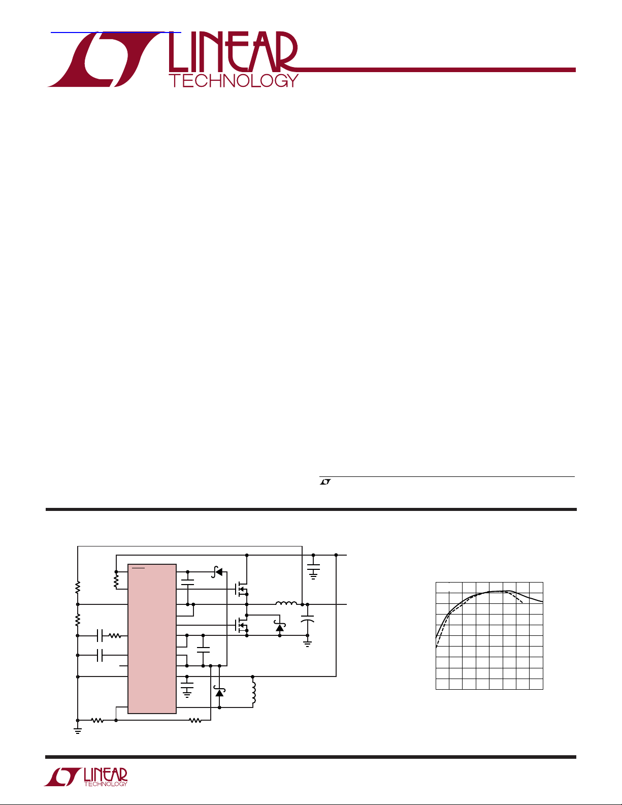
TYPICAL APPLICATIO
SHDN
330k
5.6k
10k
680pF
20k
0.1µF
12.1k
Figure 1. High Efficiency Step-Down Converter from 1.8V to 3.3V Input
I
ON
V
FB1
I
TH
RUN/SS
PGOOD
SGND
V
FB2
LTC3713
BOOST
SW1
SENSE
PGND
SENSE
INTV
SW2
TG
+
BG
–
CC
V
IN1
V
IN2
37.4k
0.33µF
4.7µF
U
CMDSH-3
10µF
MBR0520
M1
M2
L1
1.8µH
B340A
C
: PANASONIC EEFUEOD271R
OUT
4.7µH
L1: (A) PANASONIC ETQP6FIR8BFA
(B) TOKO D104C-1.8µH
M1, M2: (A) IRF7822, (B) IRF7811A
V
IN
1.8V TO 3.3V
22µF
×2
V
OUT
1.25V
OUT
10A
3713 F01a
+
C
270µF
×2
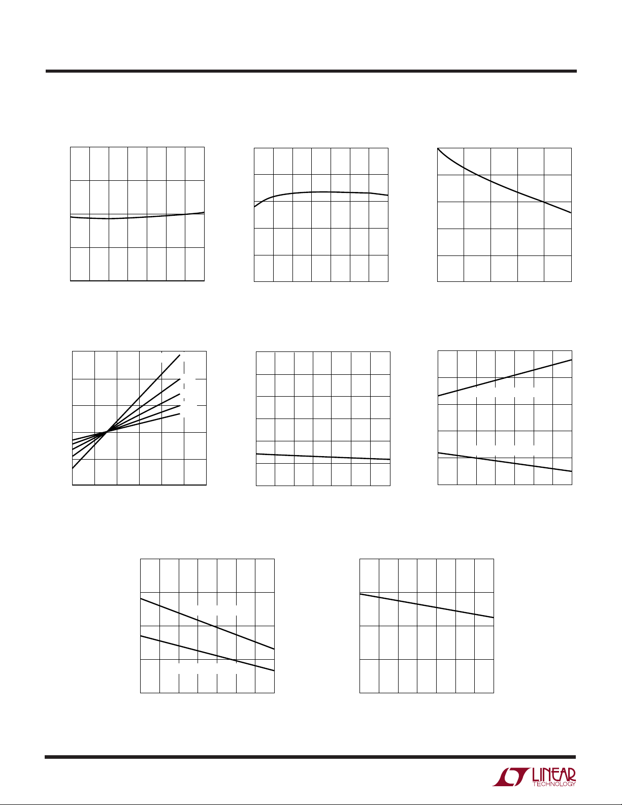
Efficiency vs Load Current
100
VIN = 2.5V
90
A
80
70
60
50
40
EFFICIENCY (%)
30
20
10
0
0.01
B
0.04 0.40
0.10
LOAD CURRENT (A)
1
3
12
7
15
3713 F01b
3713fa
1

LTC3713
WWWU
ABSOLUTE AXI U RATI GS
(Note 1)
Input Supply Voltage (V
Boosted Topside Driver Supply Voltage
(BOOST) ............................................... 42V to – 0.3V
V
, ION, SW1, SENSE+ Voltages ............. 36V to –0.3V
IN1
RUN/SS, PGOOD Voltages......................... 7V to –0.3V
FCB, VON, V
ITH, V
, SENSE– Voltages ..................... 2.7V to –0.3V
FB1
Voltages .......... INTVCC + 0.3V to –0.3V
RNG
SW2 Voltage ............................................. 36V to –0.4V
V
Voltage ................................................. V
FB2
SHDN Voltage ......................................................... 10V
TG, BG, INTVCC Peak Currents.................................. 2A
TG, BG, INTVCC RMS Currents ............................ 50mA
Operating Ambient Temperature
Range (Note 4) ................................... –40°C to 85°C
Junction Temperature (Note 2)............................ 125°C
Storage Temperature Range ................. –65°C to 150°C
Lead Temperature (Soldering, 10 sec).................. 300°C
) .......................10V to – 0.3V
IN2
IN2
+ 0.3V
UU
W
PACKAGE/ORDER I FOR ATIO
TOP VIEW
RUN/SS
1
2
V
ON
3
PGOOD
4
V
RNG
5
FCB
6
I
TH
7
SGND1
8
I
ON
9
V
FB1
10
SHDN
11
SGND2
12
V
FB2
24-LEAD PLASTIC SSOP
T
JMAX
G PACKAGE
= 125°C, θJA = 130°C/W
BOOST
24
TG
23
SW1
22
21
20
19
18
17
16
15
14
13
SENSE
SENSE
PGND1
BG
INTV
V
IN1
V
IN2
PGND2
SW2
+
–
CC
Consult LTC Marketing for parts specified with wider operating temperature ranges.
ORDER PART
NUMBER
LTC3713EG
ELECTRICAL CHARACTERISTICS
temperature range, otherwise specifications are TA = 25°C. V
The ● denotes specifications which apply over the full operating
= 15V, V
IN1
= 1.5V unless otherwise noted.
IN2
SYMBOL PARAMETER CONDITIONS MIN TYP MAX UNITS
Buck Regulator
I
Q(VIN1)
Input DC Supply Current (V
Normal 900 2000 µA
IN1
)
Shutdown Supply Current 15 30 µA
V
FB1
I
FB1
∆V
FB1(LINEREG)
∆V
FB1(LOADREG)
g
m(EA)
V
FCB
I
FCB
t
ON
t
ON(MIN)
t
OFF(MIN)
V
SENSE(MAX)
V
SENSE(MIN)
∆V
FB1(OV)
∆V
FB1(UV)
V
RUN/SS(ON)
V
RUN/SS(LE)
V
RUN/SS(LT)
Feedback Reference Voltage ITH = 1.2V (Note 3) ● 0.792 0.800 0.808 V
Feedback Current (Note 3) –5 ±50 nA
Feedback Voltage Line Regulation V
= 4V to 30V, ITH = 1.2V (Note 3) 0.002 %/V
IN1
Feedback Voltage Load Regulation ITH = 0.5V to 1.9V (Note 3) ● –0.05 –0.3 %
Error Amplifier Transconductance ITH = 1.2V (Note 3) ● 1.4 1.7 2 mS
Forced Continuous Threshold ● 0.76 0.8 0.84 V
Forced Continuous Pin Current V
= 0.8V –1 –2 µA
FCB
On-Time ION = 60µA, VON = 1.5V 200 250 300 ns
I
= 30µA, VON = 1.5V 400 500 600 ns
ON
Minimum On-Time ION = 180µA 50 100 ns
Minimum Off-Time 250 400 ns
Maximum Current Sense Threshold V
V
– V
PGND
SW
Minimum Current Sense Threshold V
– V
V
PGND
SW
V
V
V
V
RNG
RNG
RNG
RNG
RNG
RNG
= 1V, V
FB1
= 0V, V
FB1
= INTVCC, V
= 1V, V
FB1
= 0V, V
FB1
= INTVCC, V
= 0.76V ● 113 133 153 mV
= 0.76V ● 79 93 107 mV
= 0.76V ● 158 186 214 mV
FB1
= 0.84V –67 mV
= 0.84V –47 mV
= 0.84V –93 mV
FB1
Output Overvoltage Fault Threshold 5.5 7.5 9.5 %
Output Undervoltage Fault Threshold 520 600 680 mV
RUN Pin Start Threshold ● 0.8 1.5 2 V
RUN Pin Latchoff Enable Threshold RUN/SS Pin Rising 4 4.5 V
RUN Pin Latchoff Threshold RUN/SS Pin Falling 3.5 4.2 V
3713fa
2
LTC3713
ELECTRICAL CHARACTERISTICS
temperature range, otherwise specifications are TA = 25°C. V
The ● denotes specifications which apply over the full operating
= 15V, V
IN1
= 1.5V unless otherwise noted.
IN2
SYMBOL PARAMETER CONDITIONS MIN TYP MAX UNITS
I
RUN/SS(C)
I
RUN/SS(D)
UVLO V
UVLOR V
TG R
UP
TG R
DOWN
BG R
UP
BG R
DOWN
TG t
r
TG t
f
BG t
r
BG t
f
Soft-Start Charge Current V
Soft-Start Discharge Current V
Undervoltage Lockout V
IN1
Undervoltage Lockout Release V
IN1
= 0V –0.5 –1.2 –3 µA
RUN/SS
= 4.5V, VFB = 0V 0.8 1.8 3 µA
RUN/SS
Falling ● 3.4 3.9 V
IN1
Rising ● 3.5 4 V
IN1
TG Driver Pull-Up On Resistance TG High 2 3 Ω
TG Driver Pull-Down On Resistance TG Low 2 3 Ω
BG Driver Pull-Up On Resistance BG High 3 4 Ω
BG Driver Pull-Down On Resistance BG Low 1 2 Ω
TG Rise Time C
TG Fall Time C
BG Rise Time C
BG Fall Time C
= 3300pF 20 ns
LOAD
= 3300pF 20 ns
LOAD
= 3300pF 20 ns
LOAD
= 3300pF 20 ns
LOAD
Internal VCC Regulator
V
INTVCC
∆V
LDO(LOADREG)
Internal VCC Voltage 6V < VIN < 30V ● 4.7 5 5.3 V
Internal VCC Load Regulation ICC = 0mA to 20mA –0.1 ±2%
PGOOD Output
∆V
∆V
∆V
V
PGL
FB1H
FB1L
FB(HYS)
PGOOD Upper Threshold V
PGOOD Lower Threshold V
PGOOD Hysteresis V
PGOOD Low Voltage I
Rising 5.5 7.5 9.5 %
FB1
Falling – 5.5 –7.5 –9.5 %
FB1
Returning 1 2 %
FB1
= 5mA 0.15 0.4 V
PGOOD
Boost Regulator
V
IN2(MIN)
V
IN2(MAX)
I
Q(VIN2)
Minimum Operating Voltage 0.9 1.5 V
Maximum Operating Voltage 10 V
Input DC Supply Current (V
IN2
)
Normal 3 4.5 mA
Shutdown 0.01 1 µA
V
FB2
V
Feedback Voltage 0°C to 70°C 1.205 1.23 1.255 V
FB2
–40°C to 85°C ● 1.200 1.260 V
I
VFB2
∆V
FB2(LINEREG)
f
BOOST
DC
BOOST(MAX)
I
LIM(BOOST)
V
CESAT(BOOST)
I
SWLKG(BOOST)
V
SHDN(HIGH)
V
SHDN(LOW)
I
SHDN
Note 1: Absolute Maximum Ratings are those values beyond which the life
of a device may be impaired.
Note 2: TJ is calculated from the ambient temperature TA and power
dissipation PD as follows:
LTC3713EG: T
Note 3: The LTC3713 is tested in a feedback loop that adjusts V
V
Pin Bias Current ● 27 80 nA
FB2
BOOST Reference Line Regulation 1.5V ≤ VIN ≤ 10V 0.02 0.2 %/V
BOOST Switching Frequency 0°C to 70°C 1.0 1.4 1.8 MHz
–40°C to 85°C
● 0.9 1.9 MHz
BOOST Maximum Duty Cycle 82 86 %
BOOST Switch Current Limit (Note 5) 500 800 mA
BOOST Switch V
CESAT
ISW = 300mA 300 350 mV
BOOST Switch Leakage Current VSW = 5V 0.01 1 µA
SHDN Input Voltage High 1 V
SHDN Input Voltage Low 0.3 V
SHDN Pin Bias Current V
= 3V 25 50 µA
SHDN
= 0V 0.01 0.1 µA
V
SHDN
achieve a specified error amplifier output voltage (ITH).
Note 4: The LTC3713E is guaranteed to meet performance specifications
from 0°C to 70°C. Specifications over the –40°C to 85°C operating
temperature range are assured by design, characterization and correlation
= TA + (PD • 130°C/W)
J
to
FB
with statistical process controls.
Note 5: Current limit guaranteed by design and/or correlation to static test.
3713fa
3
LTC3713
DUTY CYCLE (%)
10 20 30 40 50 60 70 80
CURRENT LIMIT (mA)
3713 G06
1000
900
800
700
600
500
400
300
200
70°C
25°C
–40°C
LOAD CURRENT (A)
0.01
0
EFFICIENCY (%)
10
30
40
50
100
70
0.09
0.8
3
3713 G10
20
80
90
60
0.05
0.4
7
VIN = 3.3V
VIN = 2.5V
FIGURE 1 CIRCUIT (B)
UW
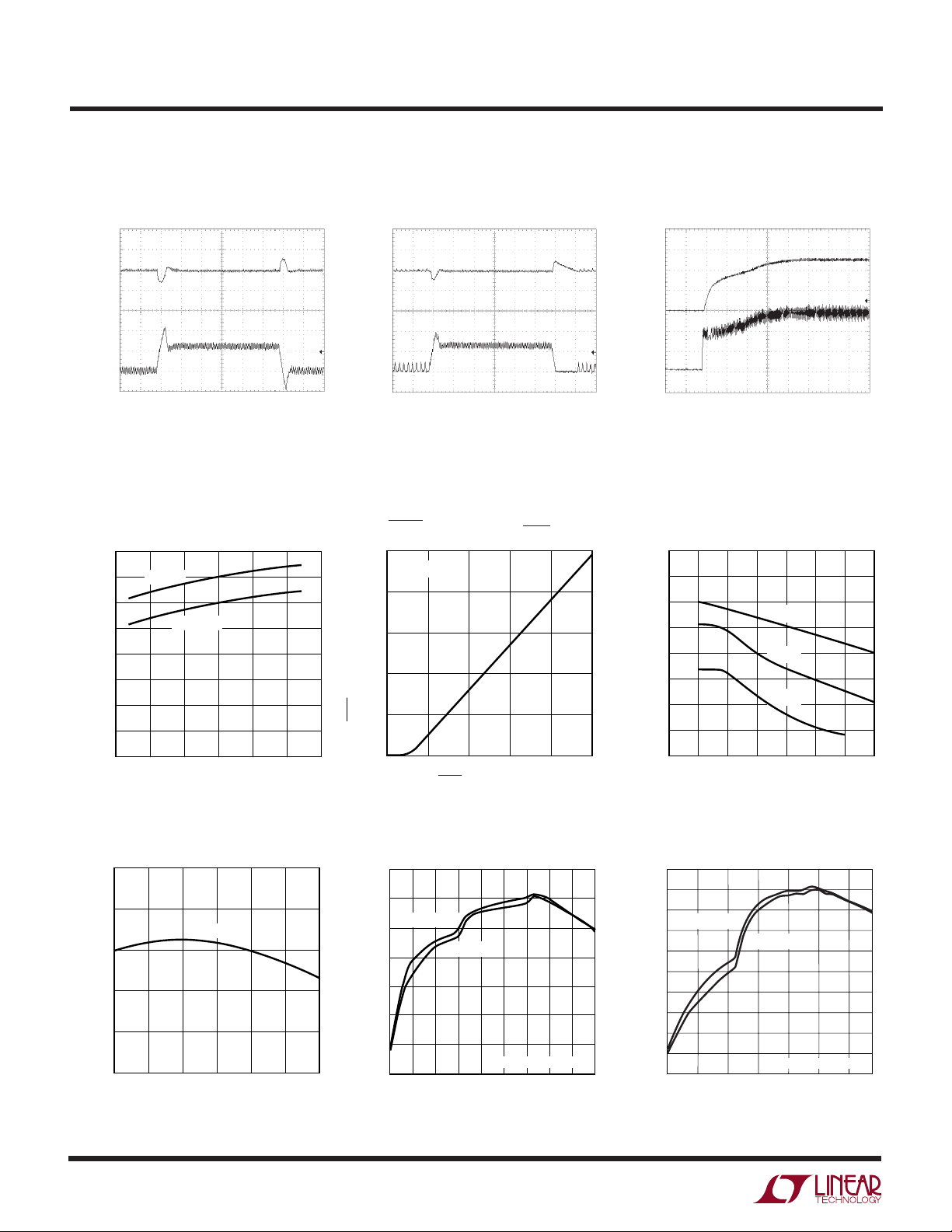
TYPICAL PERFOR A CE CHARACTERISTICS
Transient Response
V
OUT
100mV/DIV
I
L
5A/DIV
LOAD STEP 0A TO 6A
V
= 3.3V
IN
= 1.25V
V
OUT
FCB = 0V
FIGURE 1 CIRCUIT
50µs/DIV 3713 G01
Boost Converter Oscillator
Frequency vs Temperature
2.00
1.75
1.50
1.25
1.00
0.75
0.50
SWITCHING FREQUENCY (MHz)
0.25
VIN = 5V
VIN = 1.5V
0
–50 –25 0 25 50 75 100
TEMPERATURE (°C)
3713 G04
Transient Response
(Discontinuous Mode)
V
OUT
100mV/DIV
I
L
5A/DIV
LOAD STEP 600mA TO 6A
V
= 3.3V
IN
= 1.25V
V
OUT
FCB = INTV
FIGURE 1 CIRCUIT
SHDN Pin Current vs V
50
TA = 25°C
40
30
20
10
SHDN PIN BIAS CURRENT (µA)
0
012345
50µs/DIV 3713 G02
CC
SHDN
SHDN PIN VOLTAGE (V)
3713 G05
V
OUT
500mV/DIV
5A/DIV
Start-Up from Shutdown
I
L
VIN = 3.3V
V
= 1.25V
OUT
L = 1.8µH
= 540µF
C
OUT
LOAD = 0.2Ω
500µs/DIV
Boost Converter Current Limit
vs Duty Cycle
3713 G03
V
, Feedback Pin Voltage
FB2
1.25
1.24
1.23
1.22
FEEDBACK PIN VOLTAGE (V)
1.21
1.20
4
–50
–25 0 25 50 75 100
TEMPERATURE (°C)
VOLTAGE
3713 G07
Efficiency vs Load Current
(Discontinuous Mode)
100
90
VIN = 2.5V
80
70
60
EFFICIENCY (%)
50
40
30
0.01
0.04 0.07 0.1
VIN = 3.3V
0.4 41
LOAD CURRENT (A)
Efficiency vs Load Current
(Force Continuous)
FIGURE 1 CIRCUIT (B)
0.7 7 10
1713 G09
3713fa
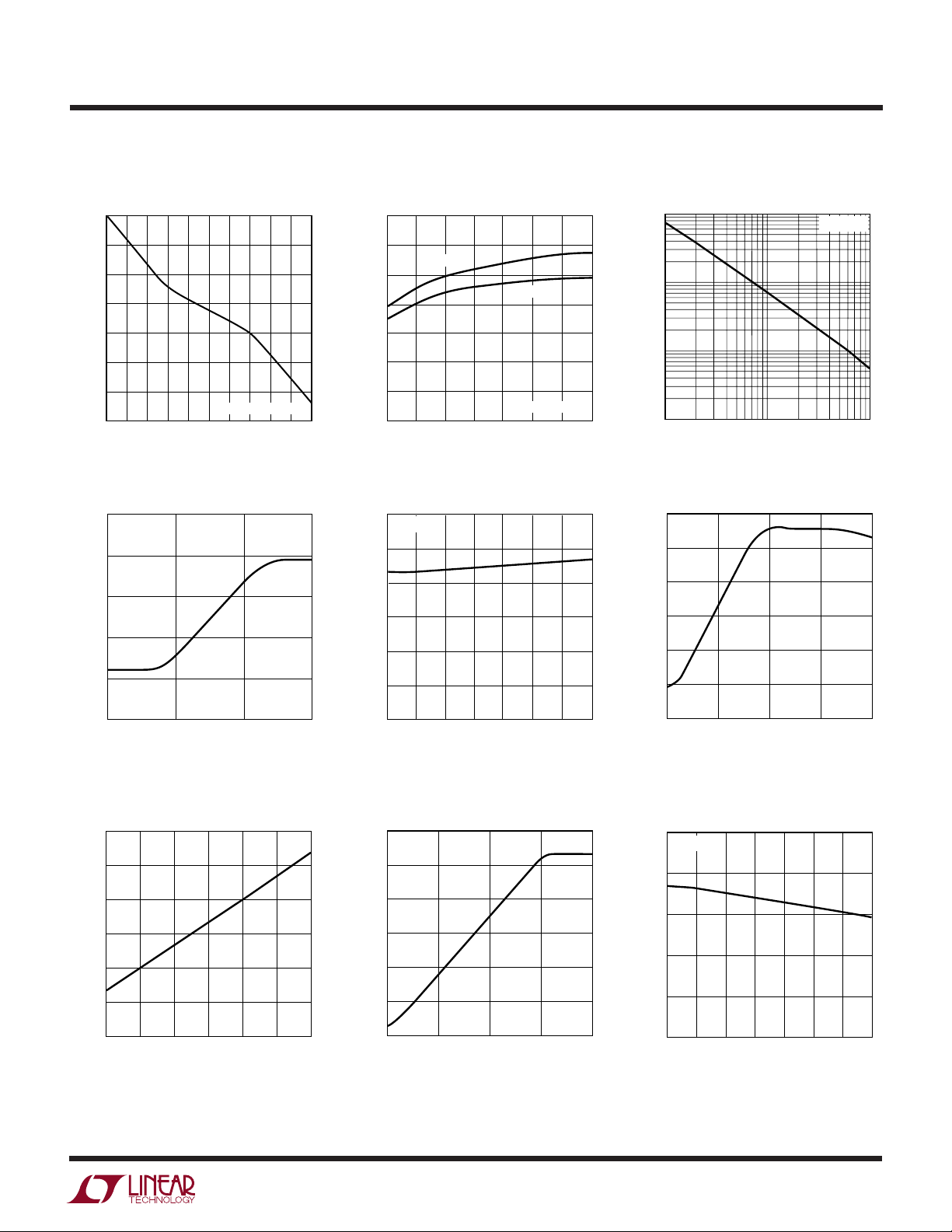
UW
VFB (V)
0
0
MAXIMUM CURRENT SENSE THRESHOLD (mV)
25
50
75
100
125
150
V
RNG
= 1V
0.2 0.4 0.6 0.8
3713 G16
TEMPERATURE (°C)
–50 –25
100
MAXIMUM CURRENT SENSE THRESHOLD (mV)
120
150
0
50
75
3713 G19
110
140
130
25
100
125
V
RNG
= 1V
TYPICAL PERFOR A CE CHARACTERISTICS
LTC3713
Load Regulation
0
–0.1
–0.2
–0.3
(%)
OUT
–0.4
∆V
–0.5
–0.6
–0.7
0
2
1
389764
LOAD CURRENT (A)
On-Time vs VON Voltage
1000
ON-TIME (ns)
800
600
400
I
ION
= 30µA
FIGURE 1 CIRCUIT
3713 G11
Frequency vs Input Voltage
350
300
0
1.5
LOAD = 6A
2.0 2.5
LOAD = 0A
FIGURE 1 CIRCUIT
3.5 4.5 5.0
3.0 4.0
INPUT VOLTAGE (V)
3713 G12
250
200
150
FREQUENCY (kHz)
100
50
105
On-Time vs Temperature
300
I
= 30µA
ION
250
200
150
ON-TIME (ns)
100
On-Time vs ION Current
10k
1k
ON-TIME (ns)
100
10
1
ION CURRENT (µA)
Current Limit Foldback
V
= 0V
VON
10 100
3713 G13
200
0
0
1
VON VOLTAGE (V)
2
3
3713 G14
Maximum Current Sense
Threshold vs V
300
250
200
150
100
50
MAXIMUM CURRENT SENSE THRESHOLD (mV)
0
0.5
0.75
1.0 1.25 1.5
V
RNG
VOLTAGE (V)
RNG
Voltage
1.75 2.0
3713 G17
50
0
–50
–25 0
TEMPERATURE (°C)
50 100 125
25 75
Maximum Current Sense
Threshold vs RUN/SS Voltage
150
125
100
MAXIMUM CURRENT SENSE THRESHOLD (mV)
= 1V
V
RNG
75
50
25
0
1.5
2 2.5 3 3.5
RUN/SS VOLTAGE (V)
3713 G15
Maximum Current Sense
Threshold vs Temperature
3713 G18
3713fa
5
LTC3713
TEMPERATURE (C)
–50
2.0
UNDERVOLTAGE LOCKOUT THRESHOLD (V)
2.5
3.0
3.5
4.0
–25 0 25 50
3713 G27
75 100 125
UW
TYPICAL PERFOR A CE CHARACTERISTICS
Feedback Reference Voltage vs
Temperature
0.82
0.81
0.80
0.79
FEEDBACK REFERENCE VOLTAGE (V)
0.78
–50
–25 0 25 50
TEMPERATURE (°C)
Current Sense Threshold vs I
Voltage
300
200
100
0
–100
CURRENT SENSE THRESHOLD (mV)
V
RNG
75 100 125
3713 G20
TH
2V
=
1.4V
1V
0.7V
0.5V
Error Amplifier gm vs
Temperature
2.0
1.8
1.6
(mS)
m
g
1.4
1.2
1.0
–50 –25
0
TEMPERATURE (°C)
50
25
FCB Pin Current vs Temperature
0
–0.25
–0.50
–0.75
–1.00
FCB PIN CURRENT (µA)
–1.25
INTVCC Load Regulation
0
–0.1
–0.2
(%)
CC
–0.3
∆INTV
–0.4
100
125
3713 G21
75
–0.5
10
0
INTVCC LOAD CURRENT (mA)
30
40
20
50
3713 G22
RUN/SS Pin Current vs
Temperature
3
2
PULL-DOWN CURRENT
1
0
FCB PIN CURRENT (µA)
–1
PULL-UP CURRENT
–200
0
6
1.0 1.5 2.0
0.5
ITH VOLTAGE (V)
RUN/SS THRESHOLD (V)
2.5 3.0
3713 G23
RUN/SS Latchoff Thresholds vs
Temperature
5.0
4.5
LATCHOFF ENABLE
4.0
3.5
3.0
–50
LATCHOFF THRESHOLD
–25 0 25 50
TEMPERATURE (°C)
–1.50
–50
–25 0
75 100 125
3713 G26
50 100 125
25 75
TEMPERATURE (°C)
3713 G24
–2
–50 –25
0
TEMPERATURE (°C)
Undervoltage Lockout Threshold
vs Temperature
50
25
75
100
125
3713 G25
3713fa

LTC3713
U
UU
PI FU CTIO S
RUN/SS (Pin 1): Run Control and Soft-Start Input. A
capacitor to ground at this pin sets the ramp time to full
output current (approximately 3s/µF) and the time delay
for overcurrent latchoff (see Applications Information).
Forcing this pin below 0.8V shuts down the device.
VON (Pin 2): On-Time Voltage Input. Voltage trip point for
the on-time comparator. Tying this pin to the output
voltage makes the on-time proportional to V
comparator input defaults to 0.7V when the pin is grounded,
2.4V when the pin is tied to INTVCC.
PGOOD (Pin 3): Power Good Output. Open-drain logic
output that is pulled to ground when the output voltage is
not within ±7.5% of the regulation point.
V
(Pin 4): Sense Voltage Range Input. The voltage at
RNG
this pin is ten times the nominal sense voltage at maximum output current and can be set from 0.5V to 2V by a
resistive divider from INTVCC. The nominal sense voltage
defaults to 70mV when this pin is tied to ground, 140mV
when tied to INTVCC.
FCB (Pin 5): Forced Continuous Input. Tie this pin to
ground to force continuous synchronous operation at low
load, to INTVCC to enable discontinuous mode operation
at low load or to a resistive divider from a secondary output
when using a secondary winding.
I
(Pin 6): Current Control Threshold and Error Amplifier
TH
Compensation Point. The current comparator threshold
increases with this control voltage. The voltage ranges
from 0V to 2.4V with 0.8V corresponding to zero sense
voltage (zero current).
SGND (Pins 7, 11): Signal Ground. All small-signal components and compensation components should connect to
this ground, which in turn connects to PGND at one point.
ION (Pin 8): On-Time Current Input. Tie a resistor from V
to this pin to set the one-shot timer current and thereby set
the switching frequency.
V
(Pin 9): Error Amplifier Feedback Input. This pin
FB1
connects the error amplifier input to an external resistive
divider from V
SHDN (Pin 10): Shutdown, Active Low. Tie to 1V or more
to enable boost converter portion of the LTC3713. Ground
to shut down.
OUT
.
OUT
. The
IN
V
(Pin 12): Boost Converter Feedback. The V
FB2
connected to INTVCC through a resistor divider to set the
voltage on INTVCC. Set INTVCC voltage according to:
V
SW2 (Pin 13): Boost Converter Switch Pin. Connect
inductor/diode for boost converter portion here. Minimize
trace area at this pin to keep EMI down.
PGND (Pins 14, 19): Power Ground. Connect these pins
closely to the source of the bottom N-channel MOSFET,
the (–) terminal of C
V
IN2
Portion of LTC3713. Must be locally bypassed.
V
IN1
PGND with an RC filter (1Ω, 0.1µF).
INTVCC (Pin 17): Internal Regulator Output. The driver and
control circuits are powered from this voltage. Decouple
this pin to power ground with a minimum of 4.7µF low ESR
tantalum or ceramic capacitor.
BG (Pin 18): Bottom Gate Drive. Drives the gate of the
bottom N-channel MOSFET between ground and INTVCC.
SENSE– (Pin 20): Negative Current Sense Comparator
Input. The (–) input to the current comparator is normally
connected to power ground unless using a resistive divider from INTVCC (see Applications Information).
SENSE+ (Pin 21): Positive Current Sense Comparator
Input. The (+) input to the current comparator is normally
connected to the SW1 node unless using a sense resistor
(see Applications Information).
SW1 (Pin 22): Switch Node. The (–) terminal of the
bootstrap capacitor CB connects here. This pin swings
from a diode voltage drop below ground up to VIN.
TG (Pin 23): Top Gate Drive. Drives the top N-channel
MOSFET with a voltage swing equal to INTVCC superimposed on the switch node voltage SW1.
BOOST (Pin 24): Boosted Floating Driver Supply. The (+)
terminal of the bootstrap capacitor CB connects here. This
pin swings from a diode voltage drop below INTVCC up to
V
IN
= 1.23V(1 + RF4/RF3)
INTVCC
and the (–) terminal of CIN.
VCC
(Pin 15): Input Supply Pin for Boost Converter
(Pin 16): Main Input Supply. Decouple this pin to
+ INTVCC.
FB2
pin is
3713fa
7
LTC3713
U
U
W
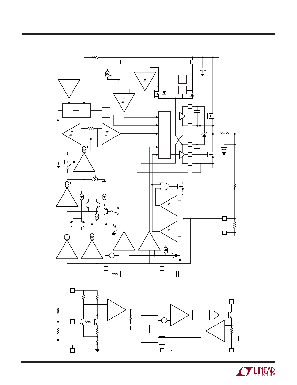
FU CTIO AL DIAGRA S
R
V
ON
2
tON = (10pF)
1.4V
V
RNG
4
0.7V
V
I
I
CMP
VON
ION
2.4V0.7V
+
–
ON
I
8
ON
1µA
R
SQ
20k
+
I
REV
–
×
3.3µA
V
V
0.8V
REF
5V
REG
BOOST
24
TG
23
SW1
22
SENSE
21
INTV
17
BG
18
PGND1
19
SENSE
20
PGOOD
3
16
IN1
+
C
B
+
CC
C
VCC
–
FCB
5
–
4.7V
+
–
0.8V
+
F
FCNT
ON
SWITCH
LOGIC
SHDN
OV
IN
C
IN
M1
D
L1
B
+
M2
V
OUT
C
OUT
R2
V
OUT2
1
240k
I
THB
+
–
×4
V
IN2
R7
(EXTERNAL)
FB2 12
R8
(EXTERNAL)
V
0.8V
15
FB2
11
Q3
Q1
Q1
SGND2
0.8V
R5
40k
0.74V
RUN/SS
Σ
UV
OV
1.2µA
6V
C
COMPARATOR
–
A2
+
SHUTDOWN
+
–
+
0.86V
–
SS
FF
RQ
S
SGND1
DRIVER
V
FB1
9
7
3713 FD01
R1
SW2
13
Q3
+
0.15Ω
–
14
PGND2
3713 FD02
3713fa
Q4
Q2
Q6
EA
–
+
R6
40k
Q2
x10
R3
30k
R4
140k
1V
Q5
R
C
C
C
RUN
SHDN
0.6V
RAMP
GENERATOR
1.4MHz
OSCILLATOR
1
SHDN
10
SS
–
+
+
–
0.6V
C
C1
I
6
TH
R
C
+
A1
g
m
–
8

OPERATIO
LTC3713
U
Main Control Loop
The LTC3713 is a current mode controller for DC/DC
step-down converters designed to operate from low input
voltages. It incorporates a boost converter with a buck
regulator.
Buck Regulator Operation
In normal operation, the top MOSFET is turned on for a
fixed interval determined by a one-shot timer OST. When
the top MOSFET is turned off, the bottom MOSFET is
turned on until the current comparator I
ing the one-shot timer and initiating the next cycle. Inductor current is determined by sensing the voltage between
the SENSE+ and SENSE– pins using the bottom MOSFET
on-resistance . The voltage on the ITH pin sets the comparator threshold corresponding to inductor valley current. The error amplifier EA adjusts this voltage by comparing the feedback signal V
with an internal 0.8V reference. If the load current increases, it causes a drop in the feedback voltage relative to
the reference. The ITH voltage then rises until the average
inductor current again matches the load current.
At low load currents, the inductor current can drop to zero
and become negative. This is detected by current reversal
comparator I
discontinuous operation. Both switches will remain off
with the output capacitor supplying the load current until
the ITH voltage rises above the zero current level (0.8V) to
initiate another cycle. Discontinuous mode operation is
disabled by comparator F when the FCB pin is brought
below 0.8V, forcing continuous synchronous operation.
The operating frequency is determined implicitly by the
top MOSFET on-time and the duty cycle required to
maintain regulation. The one-shot timer generates an ontime that is proportional to the ideal duty cycle, thus
holding frequency approximately constant with changes
in VIN. The nominal frequency can be adjusted with an
external resistor RON.
Overvoltage and undervoltage comparators OV and UV
pull the PGOOD output low if the output feedback voltage
exits a ±7.5% window around the regulation point.
Furthermore, in an overvoltage condition, M1 is turned off
which then shuts off M2, resulting in
REV
from the output voltage
FB1
trips, restart-
CMP
and M2 is turned on and held on until the overvoltage
condition clears.
Foldback current limiting is provided if the output is
shorted to ground. As V
threshold voltage I
level set by Q4 and Q6. This reduces the inductor valley
current level to one sixth of its maximum value as V
approaches 0V.
Pulling the RUN/SS pin low forces the controller into its
shutdown state, turning off both M1 and M2. Releasing
the pin allows an internal 1.2µA current source to charge
up an external soft-start capacitor CSS. When this voltage
reaches 1.5V, the controller turns on and begins switching, but with the ITH voltage clamped at approximately
0.6V below the RUN/SS voltage. As CSS continues to
charge, the soft-start current limit is removed.
INTVCC Power
Power for the top and bottom MOSFET drivers and most
of the internal controller circuitry is derived from the
INTVCC pin. The top MOSFET driver is powered from a
floating bootstrap capacitor CB. This capacitor is recharged from INTVCC through an external Schottky diode
DB when the top MOSFET is turned off.
Boost Regulator Operation
The 5V power source for INTVCC can be provided by a
current mode, internally compensated fixed frequency
step-up switching regulator that has been incorporated
into the LTC3713.
Operation can be best understood by referring to the
Functional Diagrams. Q1 and Q2 form a bandgap reference core whose loop is closed around the output of the
regulator. The voltage drop across R5 and R6 is low
enough such that Q1 and Q2 do not saturate, even when
V
is 1V. When there is no load, V
IN2
1.23V, causing VC (the error amplifier’s output) to decrease. Comparator A2’s output stays high, keeping switch
Q3 in the off state. As increased output loading causes the
V
voltage to decrease, A1’s output increases. Switch
FB2
current is regulated directly on a cycle-by-cycle basis by
the VC node. The flip-flop is set at the beginning of each
THB
drops, the buffered current
FB1
is pulled down by clamp Q3 to a 1V
FB1
rises slightly above
FB2
3713fa
9

LTC3713
OPERATIO
U
switch cycle, turning on the switch. When the summation
of a signal representing switch current and a ramp generator (introduced to avoid subharmonic oscillations at
duty factors greater than 50%) exceeds the VC signal,
comparator A2 changes state, resetting the flip-flop and
turn
ing off the switch. More power is delivered to the
output as switch current is increased. The output voltage,
attenuated by external resistor divider R7 and R8, appears
at the V
pin, closing the overall loop. Frequency com-
FB2
pensation is provided internally by RC and CC. Transient
WUUU
APPLICATIO S I FOR ATIO
A typical LTC3713 application circuit is shown in
Figure 1. External component selection is primarily determined by the maximum load current and begins with
the selection of the sense resistance and power MOSFET
switches. The LTC3713 uses the on-resistance of the
synchronous power MOSFET for determining the inductor current. The desired amount of ripple current and
operating frequency largely determines the inductor value.
Finally, CIN is selected for its ability to handle the large
RMS current into the converter and C
low enough ESR to meet the output voltage ripple and
transient specification.
Maximum Sense Voltage and V
RNG
Inductor current is determined by measuring the voltage
across a sense resistance that appears between the
SENSE+ and SENSE– pins. The maximum sense voltage
is set by the voltage applied to the V
to approximately (0.133)V
. The current mode control
RNG
loop will not allow the inductor current valleys to exceed
(0.133)V
RNG/RSENSE
. In practice, one should allow some
margin for variations in the LTC3713 and external component values and a good guide for selecting the sense
resistance is:
V
R
SENSE
=
10•
RNG
I
()
OUT MAX
An external resistive divider from INTVCC can be used to
set the voltage of the V
pin between 0.5V and 2V
RNG
is chosen with
OUT
Pin
pin and is equal
RNG
response can be optimized by the addition of a phase lead
capacitor CPL in parallel with R7 in applications where
large value or low ESR output capacitors are used.
As the load current is decreased, the switch turns on for
a shorter period each cycle. If the load current is further
decreased, the boost converter will skip cycles to maintain output voltage regulation. If the V
pin voltage is
FB2
increased significantly above 1.23V, the boost converter
will enter a low power state.
resulting in nominal sense voltages of 50mV to 200mV.
Additionally, the V
pin can be tied to SGND or INTV
RNG
CC
in which case the nominal sense voltage defaults to 70mV
or 140mV, respectively. The maximum allowed sense
voltage is about 1.33 times this nominal value.
Connecting the SENSE+ and SENSE– Pins
The LTC3713 can be used with or without a sense resistor.
When using a sense resistor, it is placed between the
source of the bottom MOSFET M2 and ground. Connect
the
SENSE+ and SENSE– pins as a Kelvin connection to the
sense resistor with SENSE+ at the source of the bottom
MOSFET and the SENSE– pin to PGND1. Using a sense
resistor provides a well defined current limit, but adds cost
and reduces efficiency. Alternatively, one can eliminate the
sense resistor and use the bottom MOSFET as the current
sense element by simply connecting the SE
NSE+ pin to the
drain and the SENSE– pin to the source of the bottom
MOSFET. This improves efficiency, but one must carefully
choose the MOSFET on-resistance as discussed in a later
section.
Applications Requiring Symmetric Current Limit
The ITH voltage has a range of 0V to 2.4V with 0.8V
corresponding to 0A. In applications in which the output
will only be sourcing current, this allows the output to sink
one third of the maximum source current. For applications
in which the output will be sourcing and sinking current,
it might be desirable to have a symmetrical output current
10
3713fa

WUUU
APPLICATIO S I FOR ATIO
+
SENSE
WITHOUT
R
SENSE
+
SENSE
–
SENSE
V
OUT
R
OS2
Figure 2. Sense Voltage Offset
V
+–
R
range with respect to zero current. This can be accomplished by introducing an offset into the sense voltage as
shown in Figure 2.
The first step in calculating the amount of required offset
voltage is to determine the maximum sense voltage.
V
SENSE
= I
OUT(MAX)
• R
SENSE
A good rule of thumb is to set the maximum sense voltage
for a current limit that is 30% greater than the maximum
source current.
OS
OS1
R
SENSE
3713 F02
LTC3713
The gate drive voltage is set by the 5V INTVCC supply.
Consequently, logic-level threshold MOSFETs must be
used in LTC3713 applications.
When the bottom MOSFET is used as the current sense
element, particular attention must be paid to its
on-resistance. MOSFET on-resistance is typically specified with a maximum value R
DS(ON)(MAX)
case, additional margin is required to accommodate the
rise in MOSFET on-resistance with temperature:
R
R
DS ON MAX
()( )
SENSE
=
ρ
T
The ρT term is a normalization factor (unity at 25°C)
accounting for the significant variation in on-resistance
with temperature, typically about 0.4%/°C as shown in
Figure 3. For a maximum junction temperature of 100°C,
using a value ρT = 1.3 is reasonable.
2.0
at 25°C. In this
The voltage on pin V
of V
V
SENSE
= V
RNG
.
SENSE
should be set based on the value
RNG
/0.133
VOS can be calculated using the following formula:
VOS = 0.6V
SENSE
The offset voltage is added as shown in Figure 2 and can
be set by choosing the values of R
VR
•
V
OS
OUT OS
=
RR
12
OS OS
1
+
The offset voltage must be scaled to V
OS1
and R
OUT
:
OS2
to avoid inter-
fering with the internal current limit foldback.
Power MOSFET Selection
The LTC3713 requires two external N-channel power
MOSFETs, one for the top (main) switch and one for the
bottom (synchronous) switch. Important parameters for
the power MOSFETs are the breakdown voltage V
threshold voltage V
transfer capacitance C
, on-resistance R
(GS)TH
and maximum current I
RSS
DS(ON)
(BR)DSS
, reverse
DS(MAX)
,
.
1.5
1.0
0.5
NORMALIZED ON-RESISTANCE
T
ρ
0
–50
Figure 3. R
0
JUNCTION TEMPERATURE (°C)
50
vs Temperature
DS(ON)
100
150
3713 F03
The power dissipated by the top and bottom MOSFETs
strongly depends upon their respective duty cycles and
the load current. When the LTC3713 is operating in
continuous mode, the duty cycles for the MOSFETs are:
V
D
TOP
D
BOT
OUT
=
V
IN
–
VV
IN OUT
=
V
IN
3713fa
11

LTC3713
f
V
VR pF
Hz
OUT
VON ON
=
[]
()10
f
VVV
VVRpF
IN OUT
VON IN ON
=
(–.)
•• ( )
07
10
WUUU
APPLICATIO S I FOR ATIO
The resulting power dissipation in the MOSFETs at maximum output current are:
P
= D
P
TOP
BOT
TOP IOUT(MAX)
+ k V
IN
= D
BOT IOUT(MAX)
2
I
Both MOSFETs have I2R losses and the top MOSFET
includes an additional term for transition losses, which are
largest at high input voltages. The constant k = 1.7A–1 can
be used to estimate the amount of transition loss. The
bottom MOSFET losses are greatest when the bottom duty
cycle is near 100%, during a short-circuit or at high input
voltage.
Operating Frequency
The choice of operating frequency is a tradeoff between
efficiency and component size. Low frequency operation
improves efficiency by reducing MOSFET switching losses
but requires larger inductance and/or capacitance in order
to maintain low output ripple voltage.
The operating frequency of LTC3713 applications is determined implicitly by the one-shot timer that controls the
on-time tON of the top MOSFET switch. The on-time is set
by the current into the ION pin and the voltage at the V
pin according to:
V
t
ON
VON
= ()10
I
ION
Tying a resistor RON from VIN to the ION pin yields an ontime inversely proportional to VIN. For a step-down
converter, this results in approximately constant frequency operation as the input supply varies:
2
ρ
T(TOP) RDS(ON)(MAX)
OUT(MAX) CRSS
2
ρ
T(BOT) RDS(ON)(MAX)
pF
f
ON
To hold frequency constant during output voltage changes,
tie the VON pin to V
. The VON pin has internal clamps
OUT
that limit its input to the one-shot timer. If the pin is tied
below 0.7V, the input to the one-shot is clamped at 0.7V.
Similarly, if the pin is tied above 2.4V, the input is clamped
at 2.4V.
Because the voltage at the ION pin is about 0.7V, the
current into this pin is not exactly inversely proportional to
VIN, especially in applications with lower input voltages.
To account for the 0.7V drop on the ION pin, the following
equation can be used to calculate the frequency:
To correct for this error, an additional resistor R
ON2
connected from the ION pin to the 5V INTVCC supply will
further stabilize the frequency.
V
07=.
5
R
V
R
ON ON2
Changes in the load current magnitude will also cause
frequency shift. Parasitic resistance in the MOSFET
switches and inductor reduce the effective voltage across
the inductance, resulting in increased duty cycle as the
load current increases. By lengthening the on-time slightly
as current increases, constant frequency operation can be
maintained. This is accomplished with a resistive divider
from the ITH pin to the VON pin and V
. The values
OUT
required will depend on the parasitic resistances in the
12
R
VON1
30k
V
OUT
R
VON2
100k
R
C
C
C
(4a) (4b)
Figure 4. Adjusting Frequency Shift with Load Current Changes
C
VON
0.01µF
V
ON
LTC3713
I
TH
INTV
R
VON1
3k
V
OUT
CC
10k
2N5087
R
VON2
10k
Q1
C
VON
0.01µF
R
C
C
C
V
ON
LTC3713
I
TH
3713 F04
3713fa

WUUU
APPLICATIO S I FOR ATIO
LTC3713
specific application. A good starting point is to feed about
25% of the voltage change at the ITH pin to the VON pin as
shown in Figure 4a. Place capacitance on the VON pin to
filter out the ITH variations at the switching frequency. The
resistor load on ITH reduces the DC gain of the error amp
and degrades load regulation, which can be avoided by
using the PNP emitter follower of Figure 4b.
Inductor L1 Selection
Given the desired input and output voltages, the inductor
value and operating frequency determine the ripple
current:
∆=
I
L
V
OUT OUT
fL
V
−
1
V
IN
Lower ripple current reduces cores losses in the inductor,
ESR losses in the output capacitors and output voltage
ripple. Highest efficiency operation is obtained at low
frequency with small ripple current. However, achieving
this requires a large inductor. There is a tradeoff between
component size, efficiency and operating frequency.
A reasonable starting point is to choose a ripple current
that is about 40% of I
OUT(MAX)
. The largest ripple current
occurs at the highest VIN. To guarantee that ripple current
does not exceed a specified maximum, the inductance
should be chosen according to:
V
fI
∆
OUT
L MAX
L
=
V
−
1
V
() ()
IN MAX
OUT
Once the value for L is known, the type of inductor must
be selected. High efficiency converters generally cannot
afford the core loss found in low cost powdered iron
cores, forcing the use of more expensive ferrite,
molypermalloy or Kool Mµ® cores. A variety of inductors
designed for high current, low voltage applications are
available from manufacturers such as Sumida, Panasonic,
Coiltronics, Coilcraft and Toko.
Schottky Diode D1 Selection
The Schottky diode D1 shown in Figure 1 conducts during
the dead time between the conduction of the power
MOSFET switches. It is intended to prevent the body diode
of the bottom MOSFET from turning on and storing charge
during the dead time, which can cause a modest (about
1%) efficiency loss. The diode can be rated for about one
half to one fifth of the full load current since it is on for only
a fraction of the duty cycle. In order for the diode to be
effective, the inductance between it and the bottom MOSFET
must be as small as possible, mandating that these
components be placed adjacently. The diode can be omitted if the efficiency loss is tolerable.
CIN and C
Selection
OUT
The input capacitance CIN is required to filter the square
wave current at the drain of the top MOSFET. Use a low
ESR capacitor sized to handle the maximum RMS current.
V
II
≅
RMS OUT MAX
()
OUT
V
IN
This formula has a maximum at VIN = 2V
I
RMS
= I
OUT(MAX)
/2. This simple worst-case condition is
V
V
IN
OUT
–1
OUT
, where
commonly used for design because even significant
deviations do not offer much relief. Note that ripple
current ratings from capacitor manufacturers are often
based on only 2000 hours of life which makes it advisable
to derate the capacitor.
The selection of C
is primarily determined by the ESR
OUT
required to minimize voltage ripple and load step
transients. The output ripple ∆V
is approximately
OUT
bounded by:
∆≤∆ +
V I ESR
OUT L
8
fC
1
OUT
Since ∆IL increases with input voltage, the output ripple is
highest at maximum input voltage. Typically, once the ESR
requirement is satisfied, the capacitance is adequate for
filtering and has the necessary RMS current rating.
Multiple capacitors placed in parallel may be needed to
meet the ESR and RMS current handling requirements.
Dry tantalum, special polymer, aluminum electrolytic and
ceramic capacitors are all available in surface mount
packages. Special polymer capacitors offer very low ESR
but have lower capacitance density than other types.
Kool Mµ is a registered trademark of Magnetics, Inc.
3713fa
13

LTC3713
WUUU
APPLICATIO S I FOR ATIO
Tantalum capacitors have the highest capacitance density
but it is important to only use types that have been surge
tested for use in switching power supplies. Aluminum
electrolytic capacitors have significantly higher ESR, but
can be used in cost-sensitive applications providing that
consideration is given to ripple current ratings and long
term reliability. Ceramic capacitors have excellent low
ESR characteristics but can have a high voltage coefficient and audible piezoelectric effects. The high Q of
ceramic capacitors with trace inductance can also lead to
signifi
cant ringing. When used as input capacitors, care
must be taken to ensure that ringing from inrush currents
and switching does not pose an overvoltage hazard to the
power switches and controller. To dampen input voltage
transients, add a small 5µF to 50µF aluminum electrolytic
capacitor with an ESR in the range of 0.5Ω to 2Ω. High
performance through-hole capacitors may also be used,
but an additional ceramic capacitor in parallel is recommended to reduce the effect of their lead inductance.
Top MOSFET Driver Supply (CB, DB)
An external bootstrap capacitor CB connected to the BOOST
pin supplies the gate drive voltage for the topside MOSFET.
This capacitor is charged through diode DB from INTV
CC
when the switch node is low. When the top MOSFET turns
on, the switch node rises to VIN and the BOOST pin rises
to approximately VIN + INTVCC. The boost capacitor needs
to store about 100 times the gate charge required by the
top MOSFET. In most applications a 0.1µF to 0.47µF X5R
or X7R dielectric capacitor is adequate.
Discontinuous Mode Operation and FCB Pin
The FCB pin determines whether the bottom MOSFET
remains on when current reverses in the inductor. Tying
this pin above its 0.8V threshold enables discontinuous
operation where the bottom MOSFET turns off when
inductor current reverses. The load current at which
current reverses and discontinuous operation begins
depends on the amplitude of the inductor ripple current
and
will vary with changes in VIN. Tying the FCB pin below
the 0.8V threshold forces continuous synchronous operation, allowing current to reverse at light loads and maintaining high frequency operation.
Fault Conditions: Current Limit and Foldback
The maximum inductor current is inherently limited in a
current mode controller by the maximum sense voltage. In
the LTC3713, the maximum sense voltage is controlled by
the voltage on the V
pin. With valley current control,
RNG
the maximum sense voltage and the sense resistance
determine the maximum allowed inductor valley current.
The corresponding output current limit is:
V
()
I
LIMIT
SNS MAX
=+∆
R
()
DS ON T
1
I
ρ
L
2
The current limit value should be checked to ensure that
I
LIMIT(MIN)
> I
OUT(MAX)
. The minimum value of current limit
generally occurs with the largest VIN at the highest ambient temperature, conditions that cause the largest power
loss in the converter. Note that it is important to check for
self-consistency between the assumed MOSFET junction
temperature and the resulting value of I
which heats
LIMIT
the MOSFET switches.
Caution should be used when setting the current limit
based upon the R
of the MOSFETs. The maximum
DS(ON)
current limit is determined by the minimum MOSFET onresistance. Data sheets typically specify nominal and
maximum values for R
reasonable assumption is that the minimum R
, but not a minimum. A
DS(ON)
DS(ON)
lies
the same amount below the typical value as the maximum
lies above it. Consult the MOSFET manufacturer for further
guidelines.
To further limit current in the event of a short circuit to
ground, the LTC3713 includes foldback current limiting. If
the output falls by more than 25%, then the maximum
sense voltage is progressively lowered to about one sixth
of its full value.
Minimum Off-time and Dropout Operation
The minimum off-time t
OFF(MIN)
is the smallest amount of
time that the LTC3713 is capable of turning on the bottom
MOSFET, tripping the current comparator and turning the
MOSFET back off. This time is generally about 250ns. The
minimum off-time limit imposes a maximum duty cycle of
tON/(tON + t
OFF(MIN)
). If the maximum duty cycle is reached,
14
3713fa

WUUU
APPLICATIO S I FOR ATIO
due to a dropping input voltage for example, then the
output will drop out of regulation. The minimum input
voltage to avoid dropout is:
tt
+
VV
IN MIN OUT
=
()
ON OFF MIN
Output Voltage Programming
A resistor divider connected between V
the output voltage according to the following equation:
R
VV
=+
08 1
OUT
.
F
R
F
()
t
ON
and V
FB1
2
1
OUT
sets
LTC3713
15
.
t
DELAY SS SS
V
=
12
CsFC
.
A
µ
When the voltage on RUN/SS reaches 1.5V, the LTC3713
begins operating with a clamp on ITH of approximately
0.9V. As the RUN/SS voltage rises to 3V, the clamp on I
is raised until its full 2.4V range is available. This takes an
additional 1.3s/µF, during which the maximum load cur-
rent is reduced. During start-up the maximum load current
is reduced until either the RUN/SS pin rises to 3V or the
output reaches 75% of its final value. The pin can be driven
from logic as shown in Figure 6. Diode D1 reduces the start
delay while allowing CSS to charge up slowly for the softstart function.
13
./
=µ
()
TH
External Gate Drive Buffers
The LTC3713 drivers are adequate for driving up to about
30nC into MOSFET switches with RMS currents of 50mA.
Applications with larger MOSFET switches or operating at
frequencies requiring greater RMS currents will benefit
from using external gate drive buffers such as the LTC1693.
Alternately, the external buffer circuit shown in Figure 5
can be used. Note that the bipolar devices reduce the
signal swing at the MOSFET gate.
10Ω
INTV
PGND
CC
Q3
FMMT619
Q4
FMMT720
GATE
OF M2
3713 F05
BOOST
Q1
FMMT619
10Ω
TG
Q2
FMMT720
SW
Figure 5. Optional External Gate Driver
GATE
OF M1
BG
Soft-Start and Latchoff with the RUN/SS Pin
The RUN/SS pin provides a means to shut down the
LTC3713 as well as a timer for soft-start and overcurrent
latchoff. Pulling the RUN/SS pin below 0.8V puts the
LTC3713 into a low quiescent current shutdown
(IQ < 30µA). Releasing the pin allows an internal 1.2µA
current source to charge up the external timing capacitor
CSS. If RUN/SS has been pulled all the way to ground,
there is a delay before starting of about:
After the controller has been started and given adequate
time to charge up the output capacitor, CSS is used as a
short-circuit timer. After the RUN/SS pin charges above
4V, if the output voltage falls below 75% of its regulated
value, then a short-circuit fault is assumed. A 1.8µA cur-
rent then begins discharging CSS. If the fault condition
persists until the RUN/SS pin drops to 3.5V, then the controller turns off both power MOSFETs, shutting down the
converter permanently. The RUN/SS pin must be actively
pulled down to ground in order to restart operation.
The overcurrent protection timer requires that the softstart timing capacitor CSS be made large enough to guarantee that the output is in regulation by the time CSS has
reached the 4V threshold. In general, this will depend upon
the size of the output capacitance, output voltage and load
current characteristic. A minimum soft-start capacitor can
INTV
CC
V
3.3V OR 5V RUN/SS
Figure 6. RUN/SS Pin Interfacing with Latchoff Defeated
IN
RSS*
D1
C
SS
(6a) (6b)
RSS*
RUN/SS
D2*
C
SS
3713 F06
*OPTIONAL TO OVERRIDE
OVERCURRENT LATCHOFF
3713fa
15

LTC3713
WUUU
APPLICATIO S I FOR ATIO
be estimated from:
CSS > C
OUT
• V
OUT
• R
(10–4 [F/V s])
SENSE
Generally 0.1µF is more than sufficient.
Overcurrent latchoff operation is not always needed or
desired. Load current is already limited during a shortcircuit by the current foldback circuitry and latchoff
operation can prove annoying during troubleshooting.
The feature can be overridden by adding a pull-up current
greater than 5µA to the RUN/SS pin. The additional
current prevents the discharge of CSS during a fault and
also shortens the soft-start period. Using a resistor to V
IN
as shown in Figure 6a is simple, but slightly increases
shutdown current. Connecting a resistor to INTVCC as
shown in Figure 6b eliminates the additional shutdown
current, but requires a diode to isolate CSS. Any pull-up
network must be able to pull RUN/SS above the 4.2V
maximum threshold of the latchoff circuit and overcome
the 4µA maximum discharge current.
INTVCC Supply
The 5V supply that powers the drivers and internal circuitry within the LTC3713 can be supplied by either an
internal P-channel low dropout regulator if VIN is greater
than 5V or the internal boost regulator if VIN is less than 5V.
The INTVCC pin can supply up to 50mA RMS and must be
bypassed to ground with a minimum of 4.7µF tantalum or
other low ESR capacitor. Good bypassing is necessary to
supply the high transient currents required by the MOSFET
gate drivers. Applications using large MOSFETs with a
high input voltage and high frequency of operation may
cause the LTC3713 to exceed its maximum junction temperature rating or RMS current rating. In continuous mode
operation, this current is I
GATECHG
= f(Q
g(TOP)
+ Q
g(BOT)
).
The junction temperature can be estimated from the
equations given in Note 2 of the Electrical Characteristics.
converter. To ensure that the ripple current doesn’t exceed
a specified amount, the inductance can be chosen according to the following equation:
V
IN MAX
2
1
V
IN MIN
2
()
L
=
–
∆
()
V
OUT BOOST
()
•
If
Diode D3 Selection
A Schottky diode is recommended for use in the boost
converter section. The Motorola MBR0520 is a very good
choice.
Boost Converter Output Capacitor
Because the LTC3713’s boost converter is internally compensated, loop stability must be carefully considered when
choosing its output capacitor. Small, low cost tantalum
capacitors have some ESR, which aids stability. However,
ceramic capacitors are becoming more popular, having
attractive characteristics such as near-zero ESR, small size
and reasonable cost. Simply replacing a tantalum output
capacitor with a ceramic unit will decrease the phase margin,
in some cases to unacceptable levels. With the addition of
a phase-lead capacitor and isolating resistor, the boost
converter portion of the LTC3713 can be used successfully with ceramic output capacitors.
Efficiency Considerations
The percent efficiency of a switching regulator is equal to
the output power divided by the input power times 100%.
It is often useful to analyze individual losses to determine
what is limiting the efficiency and which change would
produce the most improvement. Although all dissipative
elements in the circuit produce losses, four main sources
account for most of the losses in LTC3713 circuits:
Inductor Selection for Boost Converter
For the boost converter, the inductance should be 4.7µH
for input voltages less then 3.3V and 10µH for inputs
above 3.3V. The inductor should have a saturation current
rating of approximately 0.5A or greater. A guide for selecting an inductor for the boost converter is to choose a ripple
current that is 40% of the current supplied by the boost
16
1. DC I2R losses. These arise from the resistances of the
MOSFETs, inductor and PC board traces and cause the
efficiency to drop at high output currents. In continuous
mode the average output current flows through L, but is
chopped between the top and bottom MOSFETs. If the two
MOSFETs have approximately the same R
DS(ON)
, then the
resistance of one MOSFET can simply be summed with the
resistances of L and the board traces to obtain the DC I2R
3713fa

WUUU
APPLICATIO S I FOR ATIO
LTC3713
loss. For example, if R
= 0.01Ω and RL = 0.005Ω, the
DS(ON)
loss will range from 1% up to 10% as the output current
varies from 1A to 10A for a 1.5V output.
2. Transition loss. This loss arises from the brief amount
of time the top MOSFET spends in the saturated region
during switch node transitions. It depends upon the input
voltage, load current, driver strength and MOSFET capacitance, among other factors. The loss is significant at input
voltages above 20V and can be estimated from:
Transition Loss ≅ (1.7A–1) V
IN
2
I
OUT CRSS
f
3. INTVCC current. This is the sum of the MOSFET driver
and control currents.
4. CIN loss. The input capacitor has the difficult job of
filtering the large RMS input current to the regulator. It
must have a very low ESR to minimize the AC I2R loss and
sufficient capacitance to prevent the RMS current from
causing additional upstream losses in fuses or batteries.
Other losses, including C
ESR loss, Schottky diode D1
OUT
conduction loss during dead time and inductor core loss
generally account for less than 2% additional loss.
When making adjustments to improve efficiency, the input
current is the best indicator of changes in efficiency. If you
make a change and the input current decreases, then the
efficiency has increased. If there is no change in input
current, then there is no change in efficiency.
Checking Transient Response
The regulator loop response can be checked by looking
at the load transient response. Switching regulators take
several cycles to respond to a step in load current. When
a load step occurs, V
equal to ∆I
resistance of C
discharge C
(ESR), where ESR is the effective series
LOAD
OUT
generating a feedback error signal used
OUT
by the regulator to return V
During this recovery time, V
immediately shifts by an amount
OUT
. ∆I
also begins to charge or
LOAD
to its steady-state value.
OUT
can be monitored for
OUT
overshoot or ringing that would indicate a stability
problem. The ITH pin external components shown in
Figure 1 will provide adequate compensation for most
applications. For a detailed explanation of switching
control loop theory see Application Note 76.
Design Example
As a design example, take a supply with the following
specifications: VIN = 1.8V to 3.3V, V
I
OUT(MAX)
resistor with VON = V
= 6A, f = 300kHz. First, calculate the timing
:
OUT
VV
(. – . )
R
==
ON
25 07
V kHz pF
( . )( )( )
2 5 300 10
= 1.25V ±100mV,
OUT
k
240
Next, use a standard value of 237k and choose the inductor
for about 40% ripple current at the maximum VIN:
125
L
( )( . )( )
.
kHz A
300 0 4 6
V
1
–
125
.
33
.
V
=µ
108
V
H=
.
Selecting a standard value of 1µH results in a maximum
ripple current of:
125
∆=
L
.
300 1
()()
kHz H
V
1
–
µ
125
.
33
.
V
26
.
=I
V
A
Next, choose the synchronous MOSFET switch. Choosing
an IRF7811A (R
DS(ON)
= 0.013Ω, C
= 60pF, θJA =
RSS
50°C/W) yields a nominal sense voltage of:
V
SNS(NOM)
Tying V
= (6A)(1.3)(0.013Ω) = 101.4mV
to 1V will set the current sense voltage range
RNG
for a nominal value of 100mV with current limit occurring
at 133mV. To check if the current limit is acceptable,
assume a junction temperature of about 10°C above a
50°C ambient with ρ
I
LIMIT
133
≥
1 15 0 013
(. )(. )
60°C
mV
= 1.15:
1
+=
Ω
AA
2 6 10 2
(. ) .
2
and double check the assumed TJ in the MOSFET:
2
.
1 15 0 013
(. )(. )
2
Ω
P
BOT
33 1253310 2
VVVA
.–.
=
.
024
=
.
W
TJ = 50°C + (0.24W)(50°C/W) = 62°C
Now check the power dissipation of the top MOSFET at
current limit with ρ
80°C
= 1.3:
3713fa
17

LTC3713
WUUU
APPLICATIO S I FOR ATIO
125
V
.
P
=
TOP
33
1 7 3 3 10 2 60 300
+
()( )( )( )( )
068
=
10 2 1 3 0 013
()()
V
.
.. .
W
.
TJ = 50°C + (0.68W)(50°C/W) = 84°C
2
A
...
()
Ω
2
V A pF kHz
However, a 0A to 6A load step will cause an output change
of up to:
∆V
OUT(STEP)
= ∆I
(ESR) = (6A) (0.005Ω) = 30mV
LOAD
The inductor for the boost converter is selected by first
choosing an allowable ripple current. The boost converter
will be operating in discontinous mode. If we select a ripple
current of 170mA for the boost converter, then:
CIN is chosen for an RMS current rating of about 6A at
temperature. The output capacitors are chosen for a low
ESR of 0.005Ω to minimize output voltage changes due to
inductor ripple current and load steps. The ripple voltage
will be only:
∆V
OUT(RIPPLE)
= ∆I
L(MAX)
(ESR)
= (2.6A) (0.005Ω) = 13mV
C
0.1µF
C2
100pF
R
F5
10k
SS
1
RUN/SS
2
V
ON
3
PGOOD
4
V
RNG
5
FCB
6
I
TH
LTC3713
7
SGND1
8
I
ON
9
V
FB1
10
SHDN
11
SGND2
12
V
FB2
R
F4
37.4k
C
F4
1000pF
BOOST
SW1
SENSE
SENSE
PGND1
INTV
V
V
PGND2
SW2
BG
IN1
IN2
24
23
TG
22
21
+
20
–
19
18
17
CC
16
15
14
MBR0520
13
PGOOD
R
5.6k
R
10k
R
PG
100k
R
R
R2
R1
39.2k
10k
C1
R
680pF
C
20k
R
ON
F2
F1
237k
R
F3
12.1k
V
33 1
L
()(.)
170 1 4
−
.
mA MHz
33
.
5
V
V
.
47
H=
=µ
The complete circuit is shown in Figure 7.
D
B
CMDSH-3
C
B
C
IN2
4.7µF
D3
0.33µF
C
VCC
10µF
6V
X5R
M1
IRF7811A
L1
1µH
M2
IRF7811AD2B340A
L2
4.7µH
CIN: TAIYO YUDEN JMK325BJ226MM
: TAIYO YUDEN JMK212BJ475M6
C
IN2
: TAIYO YUDEN JMK316BJ106ML
C
VCC
: PANASONIC EEFUEDD271R
C
OUT
L1: TOKO D104C-1µH
L2: PANASONIC ELJPC4R7MF
+
C
OUT
270µF
×2
3713 F07
C
IN
22µF
×2
V
IN
1.8V TO 3.3V
V
OUT
1.25V
6A
18
Figure 7. Design Example: 1.25V/6A at 300kHz from 1.8V to 3.3V
3713fa

WUUU
APPLICATIO S I FOR ATIO
LTC3713
PC Board Layout Checklist
When laying out a PC board follow one of the two
suggested approaches. The simple PC board layout
requires a dedicated ground plane layer. Also, for higher
currents, it is recommended to use a multilayer board to
help with heat sinking power components.
• The ground plane layer should not have any traces and
it should be as close as possible to the layer with power
MOSFETs.
• Place CIN, C
, MOSFETs, D1 and inductor all in one
OUT
compact area. It may help to have some components
on the bottom side of the board.
• Place LTC3713 chip with Pins 13 to 24 facing the
power components. Keep the components connected
to Pins 1 to 12 close to LTC3713 (noise sensitive
components).
• Use an immediate via to connect the components to
ground plane including SGND and PGND of LTC3713.
Use several bigger vias for power components.
• Use a compact plane for switch node (SW) to improve
cooling of the MOSFETs and to keep EMI down.
• Use planes for VIN and V
to maintain good voltage
OUT
filtering and to keep power losses low.
• Flood all unused areas on all layers with copper.
Flooding with copper will reduce the temperature rise
of power component. You can connect the copper
areas to any DC net (VIN, V
, GND or to any other DC
OUT
rail in your system).
When laying out a printed circuit board, without a ground
plane, use the following checklist to ensure proper operation of the controller. These items are also illustrated in
Figure 8.
• Segregate the signal and power grounds. All small
signal components should return to the SGND pin at
one point which is then tied to the PGND pin close to
the source of M2.
• Place M2 as close to the controller as possible, keeping the PGND, BG and SW traces short.
• Connect the input capacitor(s) CIN close to the power
MOSFETs. This capacitor carries the MOSFET AC
current.
• Keep the high dV/dt SW, BOOST and TG nodes away
from sensitive small-signal nodes.
• Connect the INTVCC decoupling capacitor C
VCC
closely
to the INTVCC and PGND pins.
• Connect the top driver boost capacitor CB closely to
the BOOST and SW pins.
V
3713 F08
IN
+
V
OUT
–
3713fa
C
SS
1
RUN/SS
2
V
ON
3
PGOOD
4
V
RNG
5
C1
R
C
R
R
F2
R
F1
ON
R
F3
FCB
6
I
TH
C2
R
F5
LTC3713
7
SGND1
8
I
ON
9
V
FB1
10
SHDN
11
SGND2
12
V
FB2
R
F4
BOOST
SENSE
SENSE
PGND1
INTV
PGND2
SW1
V
V
SW2
24
C
23
TG
22
21
+
20
–
19
18
BG
17
CC
16
IN1
15
IN2
14
13
B
D
B
C
VCC
C
IN2
D3
L2 BOLD LINES INDICATE HIGH CURRENT PATHS
M1
L1
M2 D2
C
IN
C
OUT
Figure 8. LTC3713 Layout Diagram
19

LTC3713
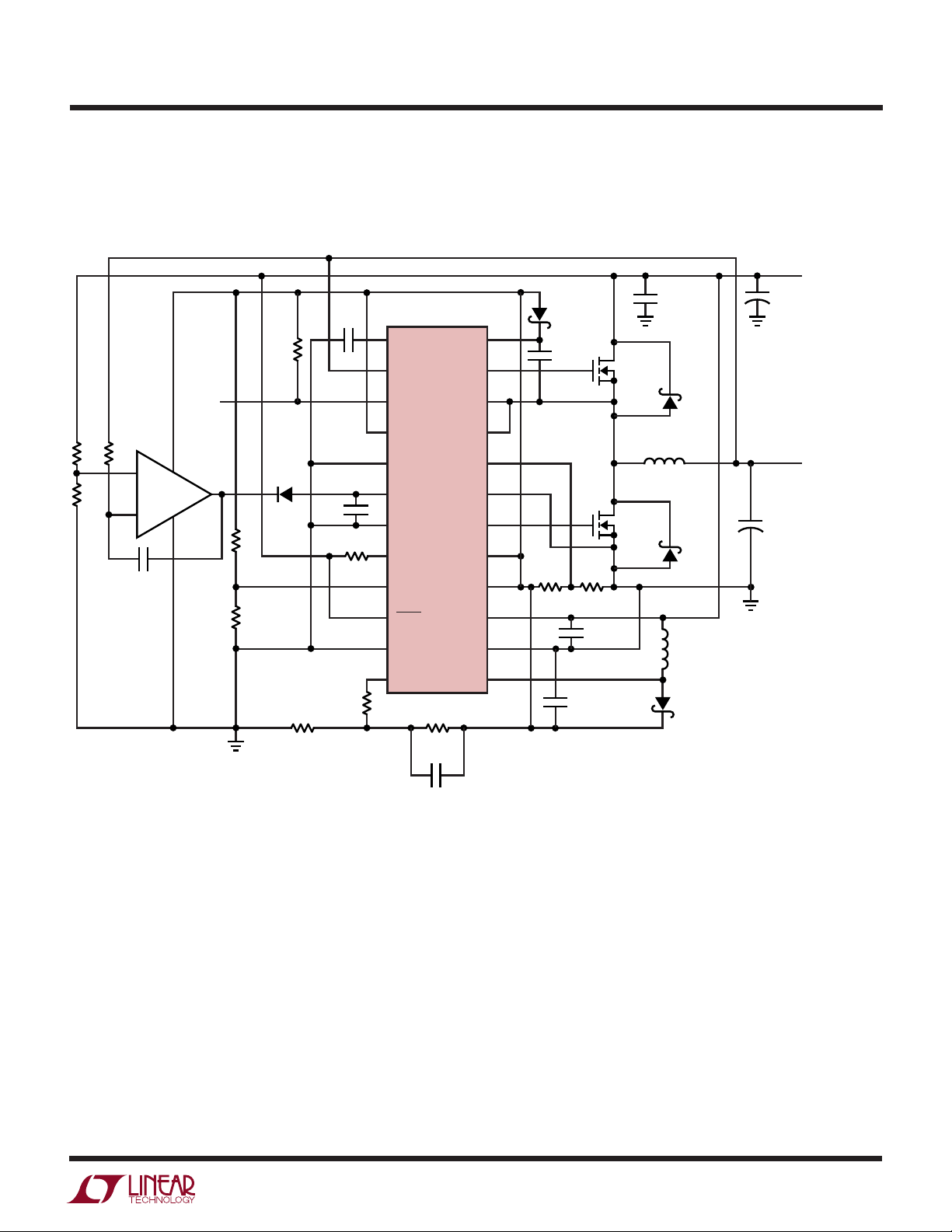
TYPICAL APPLICATIO S
C
0.1µF
C2
100pF
R
F5
10k
SS
1
2
3
4
5
6
7
8
9
10
11
12
PGOOD
R
5.6k
R
10k
R
PG
100k
R
20k
R
ON
330k
R
F3
12.1k
C
C1 680pF
F2
F1
U
RUN/SS
V
ON
PGOOD
V
RNG
FCB
I
TH
SGND1
I
ON
V
FB1
SHDN
SGND2
V
FB2
LTC3713
R
F4
37.4k
C
F4
1000pF
1.25V/±6A Bus Terminator
D
B
C
IN2
4.7µF
XR5
6.3V
D3
CMDSH-3
C
B
0.33µF
C
VCC
10µF
6.3V
X5R
BOOST
SW1
SENSE
SENSE
PGND1
INTV
V
V
PGND2
SW2
IN1
IN2
TG
BG
24
23
22
21
+
20
–
19
18
17
CC
16
15
14
13
MBR0520
R8
1.15kR768Ω
L2
4.7µH
L1
1.8µH
D1
B340A
M1
IRF7811A
+
M2
IRF7811A
C
INIA
C
INIB
: TAIYO YUDEN JMK212BJ475MG
C
IN2
C
VCC
C
OUT
L1: TOKO D104C-1.8µH
L2: PANASONIC ELJPC4R7MF
D2
B340A
: TAIYO YUDEN JMK325BJ226MM
: AVX TSPE337K010R0060
: TAIYO YUDEN JMK316BJ106ML
: PANASONIC EEFUEOD271R
C
OUT
270µF
×2
3713 TA01
C
IN1A
22µF
X5R
6.3V
×2
+
V
1.25V
±6A
OUT
V
IN
2.5V
TO 3.3V
C
IN1B
330µF
20
3713fa
TYPICAL APPLICATIO S
R
PG
100k
PGOOD
R3
R1
5k
10k
R2
10k
+
–
C1
330pF
LT1738
R
F2
10k
R
F1
1.62k
D3
MBR0520
R
12.1k
100pF
F3
U
One-Half VIN/±6A Bus Terminator
C
SS
0.1µF
1
RUN/SS
2
V
ON
3
PGOOD
4
V
RNG
5
FCB
6
I
C2
R
330k
R
F5
10k
TH
7
SGND1
8
I
ON
ON
9
V
FB1
10
SHDN
11
SGND2
12
V
FB2
LTC3713
R
F4
37.4k
C
F4
1000pF
BOOST
SW1
SENSE
SENSE
PGND1
INTV
V
V
PGND2
SW2
TG
+
–
BG
CC
IN1
IN2
LTC3713
V
IN
C
INA
22µF
M1
IRF7811A
M2
IRF7811A
D3
X5R
6.3V, ×3
L1
1µH
L2
4.7µH
3713 TA04
D2
B340A
D1
B340A
D
B
24
23
22
21
20
19
18
17
16
15
14
13
CMDSH-3
C
0.33µF
R8
4.7k
B
R7
68Ω
C
X5R, 6.3V
C
VCC1
10µF
X5R
6.3V
, 4.7µF
IN2
MBR0520
+
+
C
: TAIYO YUDEN JMK325BJ226MM
INA
C
: SANYO POSCAP 4TPB470M
INB
C
: TAIYO YUDEN JMK212BJ475MG
IN2
C
: TAIYO YUDEN JMK316BJ106ML
VCC1
C
: SANYO POSCAP 4TPB470M
OUT
L1: TOKO D104C-1µH
L2: PANASONIC ELJPC4R7MF
C
INB
470µF
×2
C
OUT
470µF
×2
1.8V TO 3.3V
V
OUT
0.9V TO 1.65V
±6A
3713fa
21

LTC3713
TYPICAL APPLICATIO S
Dual Output 1.25V/10A Buck Converter and 5V to 12V/130mA Boost Converter
U
PGOOD
R
5.6k
R
10k
1Ω
C
IN2
22µF
X5R
10V
D
B
CMDSH-3
C
B
0.33µF
C
VCC
4.7µF
X5R
6.3V
C
0.1µF
V
IN1
C
INIA
C
OUT2
4.7µF
X5R
16V
D2
B340A
22µF
X5R
6.3V
×2
+
V
OUT2
12V
130mA
C
OUT1
270µF
×2
M1
IRF7811A
L1
1.8µH
M2
IRF7811A
×2
F
L2
10µH
D3
MBR0520
5V TO 24V
V
OUT1
1.25V
10A
V
IN2
5V
SW1
V
V
SW2
TG
BG
IN1
IN2
R
F
1Ω
24
23
22
21
+
20
–
19
18
17
CC
16
15
14
13
C
R
PG
100k
C1
R
680pF
C
20k
R
ON
F2
F1
330k
R
12.3k
F3
0.1µF
C2
100pF
R
F5
10k
SS
1
10
11
12
2
3
4
5
6
7
8
9
RUN/SS
V
ON
PGOOD
V
RNG
FCB
I
TH
SGND1
I
ON
V
FB1
SHDN
SGND2
V
FB2
LTC3713
R
F4
107k
C
F4
200pF
BOOST
SENSE
SENSE
PGND1
INTV
PGND2
22
C
, C
: TAIYO YUDEN JMK325BJ226MM
INIA
IN2
: AVX TSPE337K010R0060
C
INIB
: PANASONIC EEFUEOD271R
C
OUT1
: TAIYO YUDEN EMK316BJ475ML
C
OUT2
: TAIYO YUDEN JMK212BJ475MG
C
VCC
L1: TOKO D104C-1.8µH
L2: PANASONIC ELJPC4R7MF
3713 TA02
3713fa

PACKAGE DESCRIPTIO
LTC3713
U
G Package
24-Lead Plastic SSOP (5.3mm)
(Reference LTC DWG # 05-08-1640)
1.25 ±0.12
7.8 – 8.2
0.42 ±0.03 0.65 BSC
RECOMMENDED SOLDER PAD LAYOUT
5.00 – 5.60**
(.197 – .221)
0.09 – 0.25
(.0035 – .010)
NOTE:
1. CONTROLLING DIMENSION: MILLIMETERS
2. DIMENSIONS ARE IN
3. DRAWING NOT TO SCALE
*
DIMENSIONS DO NOT INCLUDE MOLD FLASH. MOLD FLASH
SHALL NOT EXCEED .152mm (.006") PER SIDE
**
DIMENSIONS DO NOT INCLUDE INTERLEAD FLASH. INTERLEAD
FLASH SHALL NOT EXCEED .254mm (.010") PER SIDE
0.55 – 0.95
(.022 – .037)
MILLIMETERS
(INCHES)
5.3 – 5.7
° – 8°
0
7.90 – 8.50*
(.311 – .335)
2122 18 17 16 15 14
19202324
12345678 9 10 11 12
0.65
(.0256)
BSC
0.22 – 0.38
(.009 – .015)
13
7.40 – 8.20
(.291 – .323)
2.0
(.079)
0.05
(.002)
G24 SSOP 0802
Information furnished by Linear Technology Corporation is believed to be accurate and reliable.
However, no responsibility is assumed for its use. Linear Technology Corporation makes no representation that the interconnection of its circuits as described herein will not infringe on existing patent rights.
3713fa
23

LTC3713
TYPICAL APPLICATIO
R
PG
100k
PGOOD
R
F2
52.5k
+
R
10k
F1
R2
52.5k
R
20k
R1
10k
LTC1789
–
C
C2
C3
150pF
R
47.5k
C2
U
3.3V to 5V Synchronous Boost Converter
C
SS
R
F3
12.1k
R
ON
330k
R
10k
0.1µF
F5
1
RUN/SS
2
V
ON
3
PGOOD
4
V
RNG
5
FCB
6
I
TH
LTC3713
7
SGND1
8
I
ON
9
V
FB1
10
SHDN
11
SGND2
12
V
FB2
R
F4
37.4k
C
F4
1000pF
BOOST
SW1
SENSE
SENSE
PGND1
INTV
V
V
PGND2
SW2
TG
BG
IN1
IN2
24
23
22
21
+
20
–
19
18
17
CC
16
15
14
13
C
IN2
4.7µF
D
B
CMDSH-3
C
B
0.33µF
C
VCC
4.7µF
6V
X5R
L2
4.7µH
MBR0520
B340A
M2
IRF7811A
×2
D2
L1
1.8µH
M1
IRF7811A
D1
+
C
OUT1
470µF
C
OUT2
10µF
X7R
10V
C
: TAIYO YUDEN JMK325BJ226MM
INIA
C
: AVX TSPE337K010R0060
INIB
C
, C
IN2
VCC
C
3713 TA03
: SANYO POSCAP 4TPB470M
OUT1
C
: TAIYO YUDEN LMK325BJ106MN
OUT2
L1: TOKO D104C-1.8µH
L2: PANASONIC ELJPC4R7MF
V
IN
3.3V
+
C
INIA
22µF
×2
: TAIYO YUDEN JMK212BJ475MG
C
INIB
330µF
V
5V
2A
OUT
RELATED PARTS
PART NUMBER DESCRIPTION COMMENTS
LT®1613 ThinSOTTM Step-Up DC/DC Converter 1.4MHz, 1.1V < VIN < 10V
LTC1649 High Power Synchronous Step-Down Controller 3.3V Input, 1.265V ≤ V
LTC1735 High Efficiency Synchronous Switching Regulator 4V ≤ VIN ≤ 36V, 0.8V ≤ V
LTC1772 ThinSOT Current Mode Step-Down Controller Small Solution, 2.5V ≤ VIN ≤ 9.8V, 0.8V ≤ V
LTC1773 Synchronous Current Mode Step-Down Controller 2.65V ≤ VIN ≤ 8.5V, 0.8V ≤ V
550kHz Operation, >90% Efficiency
LTC1778 No R
Synchronous Step-Down Controller No Sense Resistor Required, 4V ≤ VIN ≤ 36V,
SENSE
0.8V ≤ V
OUT
≤ V
IN
LTC1876 2-Phase, Dual Synchronous Step-Down Controller with Step-Up Regulator 2.6V ≤ VIN ≤ 36V, Dual Output: 0.8V ≤ V
LTC3711 5-Bit, Adjustable, No R
Synchronous Step-Down Controller 0.925V ≤ V
SENSE
≤ 2V, 4V ≤ VIN ≤ 36V
OUT
LTC3718 Low VIN DDR Memory and SSTL Termination Power Supply 1.5V ≤ VIN ≤ 3.3V, V
LTC3778 No R
0.6V ≤ V
Synchronous Step-Down Controller Optional Sense Resistor, 4V ≤ VIN ≤ 36V,
SENSE
0.6V ≤ V
(Termination Voltage)
OUT
≤ V
OUT
IN
ThinSOT is a trademark of Linear Technology Corporation.
Linear Technology Corporation
24
1630 McCarthy Blvd., Milpitas, CA 95035-7417
(408) 432-1900 ● FAX: (408) 434-0507
●
www.linear.com
≤ 2.xV, I
OUT
≤ 6V, SSOP-16
OUT
OUT
= 1/2 VIN, V
OUT
LT/TP 1002 1K REV A • PRINTED IN USA
LINEAR TECHNOLOGY CORPORATION 2001
OUT
≤ VIN,
OUT
Up to 20A
OUT
Tracks V
≤ V
OUT
≤ (0.9)V
IN
3713fa
IN
IN
 Loading...