

L DESIGN FEATURES
NDRV
GNDPGNDVSLMT
UVLO
LTC3725
Q1
FDC2512
D1
CMPSH1-4
GATE IS
T2
183,4
5,6
1µF
162k
L1: VISHAY IHLP2525CZER0M01
L2: PULSE PA1294.910
33nF
0.03Ω
1W
HAT2165H
×2
HAT2165H
×2
T1
23.4mm × 20.1mm × 9.4mm
PLANAR
• •
• •
V
CC
33nF
15k
365k
100k
1µF
SSFLT
FB/IN
+
FS/IN
–
V
IN
+
36V
TO
72V
V
IN
–
L1
1µH
470pF
47nF
3.3k
2.2µF
FG SW IS–IS
+
1nF
2.2nF
200V
0.0012Ω
2W
SG VINNDRV
Q2
FCX491A
V
CC
GND PGND
REGSD PHASE
SLP
MODE
PT
+
PT
–
FS
FB
RUN/SS
LTC3706
ITH
2.74k
604Ω
10µF
100µF
6.3V
×2
220µF
6.3V
100k
V
OUT
+
3.3V
30A
V
OUT
–
0.1µF
5.1k
••
L2
0.85µH
1µF
100V
1µF
100V
×2
Si7450DP
5
2
4
3
10
11
7
9
1.2Ω
1/4W
T1: PULSE PA0815 (6:6:2:1)
T2: PULSE PA0297 (2:1:1)
+
VCC, PRI
VCC, SEC
V
GATE
LOAD CURRENT (A)
5
EFFICIENCY (%)
90
48V
72V
36V
92
94
25
88
86
84
10
15
20
30
Isolated Forward Controllers Offer
Buck Simplicity and Performance
Introduction
Buck converter designers have long
benefited from the simplicity, high
efficiency and fast transient response
made possible by the latest buck
controller ICs, which feature synchronous rectification and PolyPhase®
operat i o n. Unfortunately, these
same features have been difficult or
impossible to implement in the buck
converter’s close relative, the forward
converter. That is, until now. The
LTC3706/26 secondary-side synchronous controller and its companion
smart gate driver, the LTC3705/25,
make it possible to create an isolated
forward converter with the simplicity
and performance of the familiar buck
converter.
The Benefits of SecondarySide Control Made Accessible
Many isolated supplies place the
controller IC on the input (primary)
side and rely on indirect synchronous
by Charles Hawkes and Arthur Kelley
rectifier timing and optoisolator feedback to control the output (secondary).
This architecture is commonly known
as primary-side control. By contrast,
secondary-side control places the
controller IC on the secondary side,
and uses a gate-drive transformer
to directly control the primary-side
MOSFETs. This approach eliminates
the need for an optoisolator and
puts the controller where it is really
needed: with the load. This results in
a significantly faster response, taming
large-signal overshoot and reducing
output capacitance requirements.
In addition, secondary-side control
simplifies the design of the loop compensation to that of a simple buck
converter.
With the apparent advantages of
secondary-side control, why is it not
used in more isolated applications?
This is primarily because of the need
for a separate bias supply to power
up the controller on the secondary
side, since there is initially no voltage
present there. With the introduction
of the LTC3706/26 and LTC3705/25,
however, this barrier has now been
completely eliminated. All of the complex issues associated with start-up
and fault monitoring in a secondaryside control forward converter have
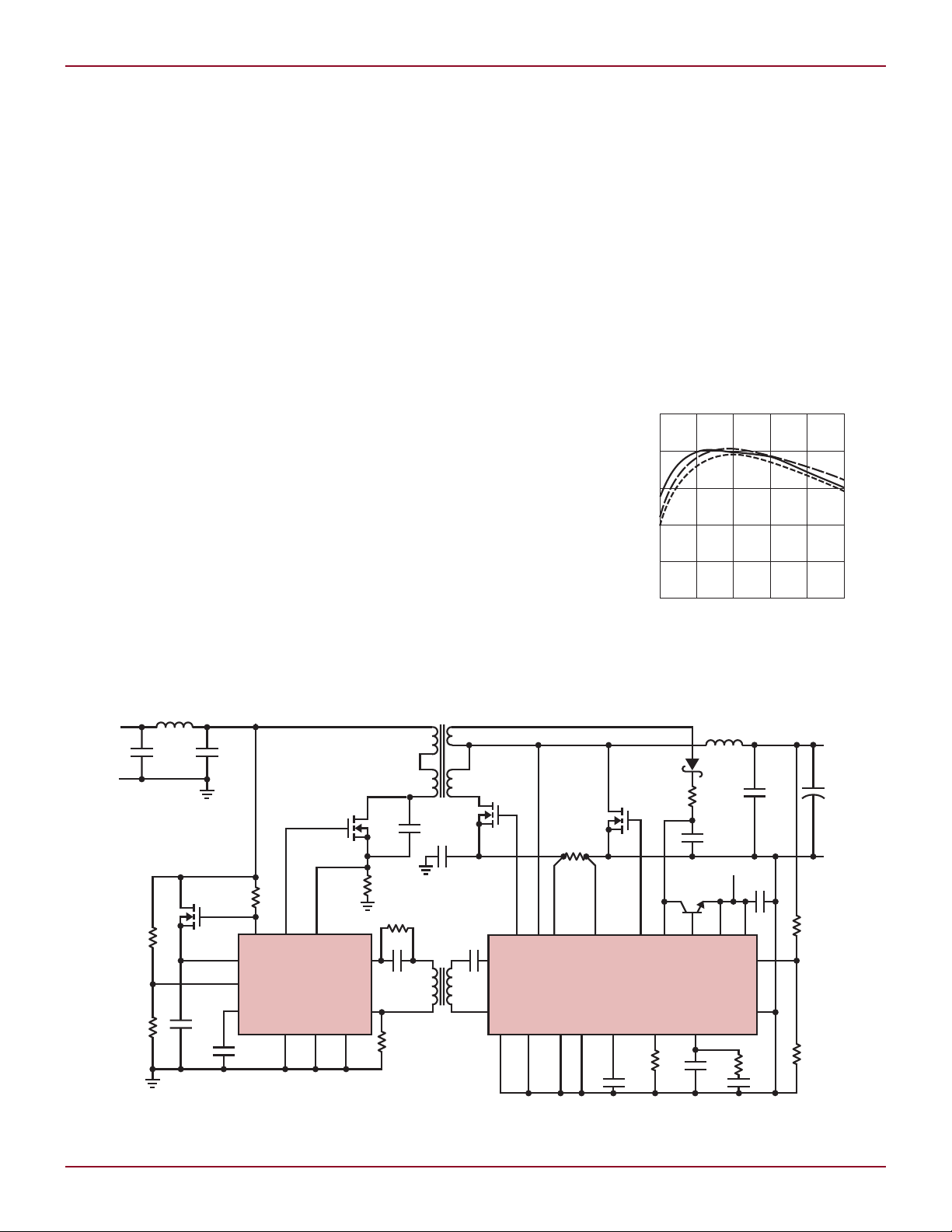
Figure 2. Efficiency of the converter
shown in Figure 1
10
Figure 1. Complete 100W single-switch high efficiency, low cost, minimum part count, isolated
telecom converter. Other output voltages and power levels require only simple component changes.
Linear Technology Magazine • March 2007
DESIGN FEATURES L
NDRV
GND PGND VSLMT
UVLO
BOOST
LTC3705
BAS21
FQT7N10
0.22µF
10µF
25V
CMPSH1-4
1.2Ω
L1
1.2µH
TG TS BG IS
T2
1µF
162k
L1: COILCRAFT SER2010-122
T1: PULSE PA0807
T2: PULSE PA0297
33nF
30mΩ
1W
2mΩ
2W
Si7336ADP
Si7336ADP
×2
T1
••
MURS120
Si7852DP
Si7852DP
MURS120
V
CC
33nF
15k
1%
365k
1%
100k
2.2µF
25V
SS/FLT
FB/IN
+
FS/IN
–
V
IN
–
V
IN
+
330µF
6.3V
×3
2.2µF
16V
680pF
CZT3019
22.6k
1%
20k
102k
1%
V
OUT
–
V
OUT
+
••
1µF
100V
x3
FG SW SG VINNDRV V
CC
GND PGND PHASE SLP MODE REGSD
PT
+
I
S
+
I
S
–
PT
–
RUN/SS
LTC3706
ITH
FB
FS/SYNC
been seamlessly integrated into these
powerful new products. Moreover, a
proprietary scheme is used to multiplex gate drive signals and DC bias
power across the isolation barrier
through a single, tiny pulse transformer. This eliminates the primary-side
bias winding that is otherwise needed.
The result is an isolated supply that
has been architected from the ground
up to achieve unprecedented simplicity
and performance. Figure 1 illustrates
how this remarkable new architecture
is used to make a complete 100W forward converter with minimal design
effort and complexity.
Family of Products Supports
Single or Dual Switch
Topologies
Ta ble 1 s u mm a ri zes how the
LTC3706/26 and LTC3705/25 products can be combined to cover a broad
range of applications. The LTC3706
is a full-featured product available
in a 24-lead SSOP package. For high
precision applications, the LTC3706
includes a 1% accuracy output voltage,
a remote-sense differential amplifier
and a power good output voltage monitor. The high voltage linear regulator
controller simplifies the design of the
bias supply, and PLL frequency synchronization with selectable phase
angle enables PolyPhase operation
with up to twelve phases. In addition,
the flexible current-sense inputs allow
Table 1. LTC3705/06/25/26 combinations
LTC3706 LTC3726
LTC3705
LTC3725
Dual-Switch,
PolyPhase
Single-Switch,
PolyPhase
Dual-Switch,
Single Phase
Single-Switch,
Single Phase
for the use of either resistive or current transformer sensing techniques.
Protection features include an output
overvoltage crowbar as well as currentlimiting and over-current protection.
The 16-lead LTC3726 does not include
the remote voltage sensing or linear
regulator features, so it is more suitable for a single phase application.
Both the LTC3706 and the LTC3726
have a selectable maximum duty cycle
limit of either 75% or 50% to support a
single or dual-switch forward converter
application, respectively.
The LTC3725 primary driver is
intended for use in single-switch
forward converter. The LTC3725 includes a start-up linear regulator and
an integrated bridge rectifier for bias
generation. Protection features include
volt-second limit, over-current protection and a fault monitoring system that
detects a loss of encoded gate-drive
signal from the signal transformer.
The LTC3705 is a dual-switch forward
driver, and includes an 80V (100V
transient) high side gate driver. The
integration of this high side driver into
the LTC3705 greatly facilitates the use
of the simple and robust dual switch
forward converter topology. Figure 3
shows a typical dual-switch converter
application using the LTC3705 and
the LTC3706.
Table 2 highlights some of the relative merits of using either single or dual
switch forward converter topologies.
In general, for applications that have
a limited input voltage variation, or
where a robust and simple design is
a priority, the dual-switch forward
converter may be preferred. For a wide
input voltage application (greater than
2:1), or whenever a lower cost or size
justifies the complication of the transformer reset design, a single-switch
forward should be used.
Bringing the Power of
PolyPhase to Isolated Supplies
The LTC3706/26 defies typical forward
converter limits by allowing simple
implementation of a PolyPhase current
share design. PolyPhase operation
allows two or more phase-interleaved
power stages to accurately share the
load. The advantages of PolyPhase
current sharing are numerous, including much improved efficiency, faster
transient response and reduced input
and output ripple.
The LTC3706/26 supports standard output voltages such as 5V, 12V,
28V and 52V as well as low voltages
down to 0.6V. Figure 4 shows how
11
Linear Technology Magazine • March 2007
Figure 3. Isolated forward converter for 36V–72V input to 3.3V/20A out

L DESIGN FEATURES
SSP
V
IN
+
V
IN
–
V
IN
+
V
IN
–
V
OUT
+
1.2V/100A
V
OUT
–
V
OUT
+
V
OUT
–
SYNC
LTC3705/LTC3706
36V-72VIN TO 1.2V
OUT
50A SUPPLY
ITH SSSV
BIAS
SSP
V
IN
+
V
IN
–
V
OUT
+
V
OUT
–
SYNC
LTC3705/LTC3706
36V-72VIN TO 1.2V
OUT
50A SUPPLY
ITH SSSV
BIAS
I
LOUT1
I
LOUT2
10A/DIV
10µs/DIV
V
OUT
0.5V/DIV
2ms/DIV
SECONDARY-SIDE MODE
PRIMARY-
SIDE MODE
V
IN
V
CCPRI
V
CCPRI
SUPPLIED BY Q1
V
GATE
CONTROLLED BY LTC3706
V
GATE
CONTROLLED BY LTC3725
V
CCPRI
SUPPLIED BY
TRANSFORMER T2
V
GATE
V
OUT
V
CC,SEC
V
PT+,VPT–
easy it is to parallel two 1.2V supplies
to achieve a 100A supply. Figure 5
shows excellent output inductor current tracking during a 0A to 100A load
current step and the smooth handoff
during start-up to secondary-side control at approximately V
= 0.25V.
OUT
Anatomy of a Start-Up:
A Simple Isolated 3.3V,
30A Forward Converter
The circuit of Figure 1 shows a
complete 100W, one-switch forward
converter. In this example, the
LTC3706 controller is used on the
secondary and the LTC3725 driver
with self-starting capability is used
on the primary. This design features
off-the-shelf magnetics and high efficiency (see Figure 2). The start-up
behavior of this supply is illustrated
in Figure 6. When input voltage is
first applied, the LTC3725 uses Q1
to generate a bias voltage V
begins a controlled soft-start of the
output voltage. As the output voltage
begins to rise, the LTC3706 secondary controller is quickly powered up
by using T1, D1 and Q2 to generate
V
V
. As shown in Figure 6, the
CC,SEC
voltage rises very quickly as
CC,SEC
compared with the output voltage
V
of the converter. The LTC3706
OUT
CC,PRI
, and
Table 2. Single and dual switch forward converter relative merits
Requirement Single-Switch Dual-Switch
Simple Design
Requires Design
Transformer Reset Circuit
to Prevent Saturation
Wide Input Supply Range
(>2:1)
High Efficiency
Low Switch Voltage Stress
Low Cost
Small Size
75% Max Duty
Good
Can be 2 × VIN or Greater
One FET
One FET and Better
Transformer Utilization
then assumes control of the output
voltage by sending encoded PWM gate
pulses to the LTC3725 primary driver
via signal transformer T2. As soon as
the LTC3725 begins decoding these
PWM gate pulses, it shuts down the
linear regulator by tying NDRV to VCC
and begins extracting bias power for
V
from the signal transformer T2.
CC,PRI
This complete transition from primary
to secondary control occurs seamlessly
at a fraction of the output voltage. From
–
+
Reset Circuit not
Required—Can’t Saturate
+
–
50% Max Duty
+
+
Good
–
+
+
Limited to V
–
IN
Two FETs
+
–
Two FETs and 50%
Transformer Utilization
that point on, operation and design
simplifies to that of a simple buck
converter. Even the design and optimization of the feedback loop makes use
of the familiar and proven OPTI-LOOP®
compensation techniques.
A 10V–30V Input, 15V Output
at 5A Forward Converter
Figure 7 highlights the flexibility of
the LTC3706 and LTC3725 by illustrating a 12V/24V input application.
Figure 4. Paralleling supplies for higher power operation
12
Figure 5. 1.2V, 100A load current step
(top trace) and start-up (bottom trace)
Figure 6. Anatomy of a start-up
Linear Technology Magazine • March 2007

DESIGN FEATURES L
NDRV
GND PGND VSLMT
UVLO
GATE
LTC3725
2.2nF
250VAC
C3
2.2nF
100V
220pF
200V
68pF
L1
13µH
10Ω
0.5W
150Ω
174Ω
IS
T2
1µF
68pF
68pF
162k
470pF
L1: PULSE PA1961.133
T1: PULSE PA0810
T2: PULSE PA0297
C1: NIPPON CHIMICON EMZA500ADA221MUA0G
C2: TAIYO YUDEN GMK325BJ106MN
C3: TAIYO YUDEN TMK325BJ106MM
C4: SANYO OSCON 16SVP180MX
Q1: FMMT38C
Q2: MMBFJ201
Q3: ZVN3320F
Q4: FDMS2572 ×2
Q5: FMMT 618
Q6: FMMT 718
Q7: MMBT 2907A
33nF
5mΩ
2W
6mΩ
1W
Si7852DP
Q7
Q5
Q4
Q6
T1
1:3
2:1
V
CC
68nF
383k
75k
Q1
R1
10k
1µF
25V
SS/FLT
FB/IN
+
FS/IN
–
V
IN
–
V
IN
+
C4
180µF
16V
C6
10µF
200V
C3
10µF
25V
×2
10µF
16V
R2
8.66k
1nF
470pF
FG SW SG VINNDRV V
CC
GND PGND PHASE SLP MODE REGSD
PT
+
I
S
+
I
S
–
PT
–
RUN/SS
LTC3706
ITH
100k
43.2k
1.07k
1%
25.5k
1%
V
OUT
–
V
OUT
+
330pF
33pF
D2 BAT54
C5
0.1µF
R3
33k
0.5W
D1
ES1C
FCX1051A
FB
FS/SYNC
0.1µF
1nF
••
C1
220µF
50V
×2
C2
10µF
35V
×5
100Ω100Ω
100Ω
5.1kΩ
301Ω
IRF6648
×2
Q3
100Ω
Q2
LOAD CURRENT (A)
0
85
90
95
4
2 6
75
80
EFFICIENCY (%)
VIN = 12V
VIN = 24V
V
OUT
200mV/DIV
I
OUT
5A/DIV
20µs/DIV
VIN = 12V
V
OUT
= 15V
LOAD STEP = 0A TO 5A
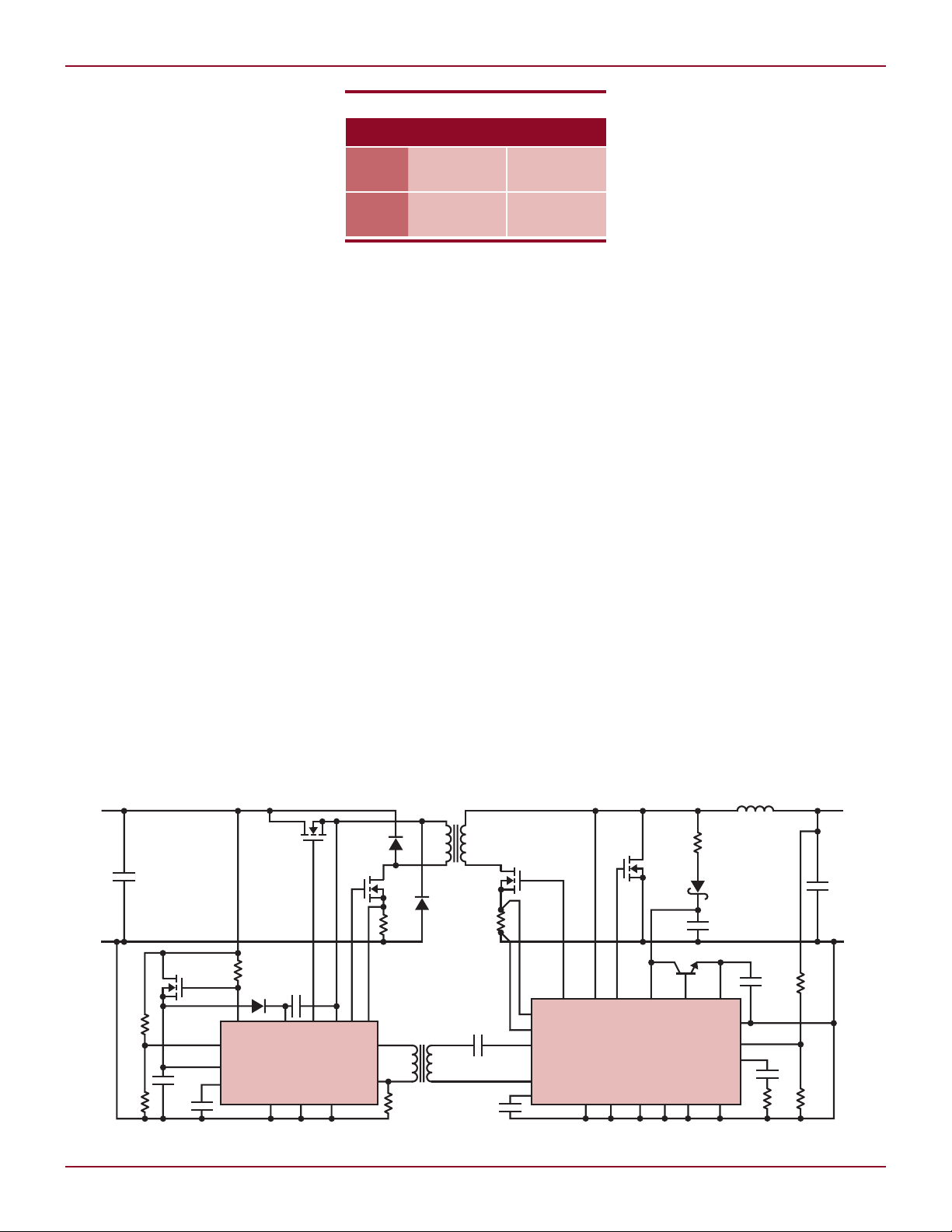
Figure 7. Isolated forward converter for 10V–30V input to 15V/5A out
In this circuit, the main transformer
T1 is used to step up the voltage so
that the output can be either higher
or lower than the input. This circuit
is an excellent alternative to a flyback
converter where higher efficiency or
lower noise is a priority.
The UVLO on the LTC3725 has been
set to turn on at V
V
= 7.5V, and a linear regulator (Q1)
IN
= 9.5V and off at
IN
is used to establish bias for start-up.
Note that the LTC3725 requires that
the NDRV pin be at least 1V above
the VCC pin for proper linear regulator
operation. To meet this requirement,
while providing the lowest possibly
dropout voltage, a darlington transistor is used (Q1). JFET Q2 is used to
provide adequate bias current for the
NDRV pin at low input voltage, while
limiting the maximum current seen at
high input voltage. R11 is needed to
prevent back-feeding of current from
the NDRV pin into base of Q1 (and
Linear Technology Magazine • March 2007
gate of Q2) during normal operation
when V
less than 12V.
On the secondary side, the output
voltage is used directly as a source
of bias voltage for the LTC3706. This
is possible for output voltages of 9V
or greater. Q3 is used to limit the
CC
= V
= 12V and VIN is
NDRV
peak voltage seen by the SW pin on
Figure 8. Transient response
of the circuit in Figure 7
the LTC3706, while still allowing the
detection circuits in the LTC3706 to
function normally. Capacitor C3 is
used to establish the resonant reset
of the main transformer T1 during the
off-time of the primary-side switches.
In order to reduce the inrush current
during start-up, D2, R2 and C5 are
continued on page 39
Figure 9. Efficiency of
the circuit in Figure 7
13

DESIGN IDEAS L
R1
200Ω
R3
200Ω
R4
200Ω
R2
200Ω
5V
PECL LEVELS
1/4 MC10H350
PECL-TTL TRANSLATOR
TTL OUTPUT
OUT
OPTION
700mV
PP
(DIFFERENTIAL)
MINIMUM
(INPUT
CIRCUITRY
OMITTED)
5V
OV
DD
OGND
+
–
LT6411
5V5V
LT1715
20µs/DIV
V
OUT
50mV/DIV
INDUCTOR
CURRENT
5A/DIV
Single-Ended Output
The LT6411 produces a differential
output, but if a single-ended logic
output is needed, there are multiple
options for data conversion. One such
way is shown in Figure 8, in which
the MC10H350 PECL-TTL translator
performs the conversion. To translate
the voltage levels from the LT6411 to
PECL input voltage levels, two resistive dividers level-shift and attenuate
the output signal of the LT6411. Alternatively, a high speed comparator
such as Linear Technology’s LT1715
can also perform this task without the
level-shifting resistors.
Conclusion
The LT6411 is a dual high speed amplifier with flexible features and superb
AC characteristics, making it suitable
for use as a high data rate receiver.
The ability to select different gain
configurations with minimal external
components makes the LT6411 easy
to use. Its small footprint and low
power consumption allow it to fit into
Figure 8. If a single-ended output is needed, there are many options available for translators.
One example is ON Semiconductor’s MC10H350 PECL-TTL translator. The 200Ω resistors shift
the output of the LT6411 up to PECL voltage levels. Alternatively, a level-translating comparator
such as the LT1715 could be used to give a variety of logic output levels.
almost any application without painful
compromises, especially for portable
or peripheral applications where space
and power are at a premium.
L
LT3740, continued from page 36
The LT3740 uses a valley mode current control system that boasts a fast
response to load changes. As shown
in Figure 3, this design responds to
0A–10A step load change in 10µs,
yielding a voltage transient of less
than 50mV.
Soft-Start
The LT3740 is also equipped with a
flexible soft-start design that allows for
either ramped current or tracking. If
the XREF pin is held above 1V, and an
RC timer is applied to the SHDN pin,
the converter soft-starts by ramping
the current available to the load. If the
SHDN pin is high, enabling the chip,
and a 0V to 0.8V tracking signal is
applied to the XREF pin, the internal
reference of the LT3740 follows the
tracking signal.
LTC3706/26, continued from page 13
used to provide a gradual increase
in peak current during the soft-start
interval. The circuit of Figure 7 also
includes an optional falling-edge delay
circuit on the gate of synchronous
switch Q4. This delay has been used
to optimize the dead time for this
specific application, thereby improving
Linear Technology Magazine • March 2007
Conclusion
The LT3740 is a synchronous buck
controller that boasts a rich feature set
which allows the designer to optimize
power and volumetric efficiency by exploiting the advantages of a low input
voltage. Through a combination of its
Figure 3. Output voltage and inductor current response to a
0A–10A step load transient applied to the circuit in Figure 1
the efficiency by about 1%. Figure 8
shows the transient response that is
achieved using the circuit of Figure 7,
and Figure 9 shows the efficiency at
V
IN
Conclusion
The new LTC3706/26 controller and
LTC3705/25 driver bring an un-
= 12V and V
= 24V.
IN
onboard boost regulator, user programmable current limit thresholds,
fast transient response and flexible
soft-start system, the designer can
produce a small, efficient, full featured
converter.
L
precedented level of simplicity and
performance to the design of isolated
power supplies. Each controller-driver
pair works in concert to offer high
efficiency, low cost solutions using
off-the-shelf components. The devices
are versatile and easy to use, covering
a broad range of forward converter
applications.
L
3939
 Loading...