

L DESIGN FEATURES
SWI/O
I/O
RESET
DA
FB
R
T
SYNC
fSW = 700kHz
WDI
RST
WDO
V
IN
µP
EN/UVLO
V
IN
4.5V TO 36V
TRANSIENT TO 60V
3.3V
800mA
100k
C
WDT
10nF
t
WDU
= 182ms
t
WDL
= 5.9ms
12µH
10pF
22µF
0.1µF
MBRM140
316k
GND
21k
LT3689
BST
OUT
C
POR
C
WDT
2.2µF
C
POR
68nF
t
RST
= 157ms
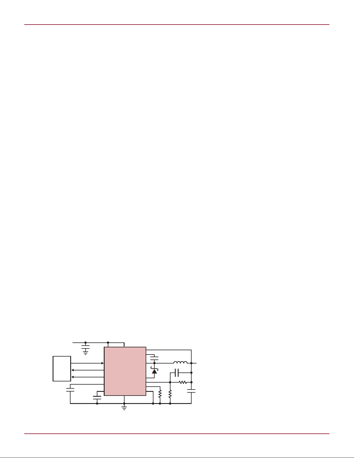
Industrial/Automotive Step-Down
Regulator Accepts 3.6V to 36V
and Includes Power-On Reset and
Watchdog Timer in 3mm × 3mm QFN
Introduction
As the number of microprocessors in
automotive and industrial applications continues to expand, so does the
need for rugged step-down regulators
that can operate over a wide input
voltage range and withstand high
voltage transients and output shorts.
Microprocessor-based applications
also require supervisory functions,
such as power-on reset (POR) and
watchdog timing, to ensure high system reliability. The regulator must
have high efficiency at light loads
to increase battery life. The LT3689
delivers all of these features in tiny
16-pin 3mm × 3mm QFN and 16-pin
MSOP packages.
Features of the LT3689
Step-Down Regulator
The LT3689 employs a constant frequency, current mode architecture to
provide 800mA of continuous output
current. The part operates from a
wide 3.6V to 36V input range and can
protect itself from input transients up
to 60V. It is internally compensated,
which helps to lower the external component count. The switching frequency
can be set anywhere between 350kHz
and 2.2MHz by tying a resistor from
24
Figure 1. LT3689 typical application circuit with reset time
set to 157ms and watchdog timeout period set to 182ms
the RT pin to ground, allowing the designer to optimize component size and
efficiency. The switching frequency can
also be synchronized to an external
clock for noise sensitive applications.
An external resistor divider programs
the output voltage to any value above
the part’s 0.8V reference. Also, the
boost diode is integrated into the IC
to minimize solution size and cost.
Figure 1 shows a typical application
of LT3689.
Soft-Start and Output
Short Circuit Protection
The LT3689 includes a soft-start feature that limits the maximum inrush
current during start-up and recovery
from fault conditions. The soft-start
circuit ramps up the peak switch
current limit in approximately 150µs,
reducing the peak input current.
The DA pin is used to monitor the
current in the catch diode. If the catch
diode current at the end of switch
cycle is higher than the DA current
limit then the part delays the switch
turn-on until the catch diode current
drops below the DA current limit. This
protects the LT3689 in the face of
inductor current runaway situations,
by Ramanjot Singh
especially during output overload or
short at high switching frequencies
with high input voltages and small
inductor values. Other protection
features such as frequency foldback,
cycle-by-cycle current limit, and thermal shutdown together ensure that
the part is not damaged by excessive
switch currents during startup, overload or short circuit.
Pin Selectable Modes of
Operation: Low Ripple
Burst Mode Operation
and Pulse-Skipping Mode
Two modes of operation can be selected
through the SYNC pin. Applying a logic
low to the SYNC pin enables the low
ripple Burst Mode® operation, which
maintains high efficiency at light loads
while keeping output ripple low. In
Burst Mode operation, the LT3689
delivers single cycle bursts of current
to the output capacitor followed by
sleep periods. Between bursts, all circuitry associated with controlling the
output switch is shutdown, reducing
the VIN pin and OUT pin currents in
a typical application to a mere 50µA
and 75µA, respectively. As the load
current decreases to a no load condition, the percentage of sleep time
increases, thus decreasing average
input current.
A logic high on SYNC disables Burst
Mode operation, allowing the part to
skip pulses at light loads. The advantage of this pulse-skipping mode over
Burst Mode operation is that the part
continues to switch at the programmed
frequency (set by RT) down to very low
load currents, above 15mA at 12V
in a typical application.
Linear Technology Magazine • March 2009
IN
DESIGN FEATURES L
POR COMPARATOR OVERDRIVE VOLTAGE AS PERCENTAGE
OF RESET THRESHOLD, V
RST
(%)
0.10
400
TRANSIENT DURATION (µs)
500
600
700
800
1.00 10.00 100.00
300
200
100
0
RESET OCCURS
ABOVE THE CURVE
50ms/DIV
V
OUT
2V/DIV
C
POR
1V/DIV
RST
2V/DIV
t
RST
= 165ms
C
POR
= 71.3nF
Programmable
Undervoltage Lockout
The LT3689 can be shutdown by pulling the EN/UVLO pin below 0.3V. In
shutdown, quiescent current is less
than 0.5µA. The EN/UVLO pin can
also be used to perform an accurate
undervoltage lockout (UVLO) function.
A resistor divider from VIN pin can be
used to program the UVLO threshold
of the circuit using the 1.26V accurate
threshold of the EN/UVLO pin. A 4µA
current hysteresis on this pin is also
provided to allow the user to program
desired voltage hysteresis. The LT3689
also has an internal UVLO that prevents the part from switching if VIN
pin ever goes below 3.3V (typical). The
part only starts switching when VIN is
higher than 3.4V and EN/UVLO pin
is above the 1.26V threshold.
Low Dropout
The LT3689 features low dropout for
output voltages above 3V. The minimum operating voltage of the device
is determined either by the LT3689’s
internal undervoltage lockout or
by its maximum duty cycle. Unlike
many buck regulators, the LT3689
can extend its duty cycle by staying
on for multiple cycles, provided that
the boost capacitor is charged above
the minimum voltage of 2.5V. Eventually, after several switching cycles, the
boost capacitor discharges. Internal
circuitry detects this condition and
charges the boost capacitor only when
needed. Also, a bigger boost capacitor
allows even higher duty cycle, allowing extremely low dropout operation.
The dropout voltage for a 5V typical
application is about 400mV at 200mA
load and 900mV at 800mA load.
Figure 2. Power-on reset feature of LT3689
Linear Technology Magazine • March 2009
Power-On Reset (POR)
Many microprocessor -based applications powered by the output
of a switching regulator must know
when the regulator output is ready
and stable before the microprocessor
starts operating. Likewise, once running, the electronic system must be
warned when the regulator output has
dropped below a minimum tolerable
threshold, such as during overload or
shutdown conditions. This is required
to prevent unreliable operation and to
allow the microprocessor to perform
housekeeping operations before power
is completely lost.
The LT3689’s accurate internal
voltage reference and glitch immune
precision POR comparator and timer
circuit feed these specific needs of
microprocessor -based applications.
The switcher’s output voltage must
be above 90% of programmed value
for its RST pin to remain high (refer
to Figure 2). The LT3689 asserts
RST during power-up, power-down
and brown-out conditions. Once the
output voltage rises above the RST
threshold, the adjustable reset timer
is started and RST is released after the
reset timeout period. On power-down,
once output voltage drops below RST
threshold, RST is held at a logic low.
The reset timer is adjustable using an
external capacitor. The RST pin has a
weak pull up to the OUT pin.
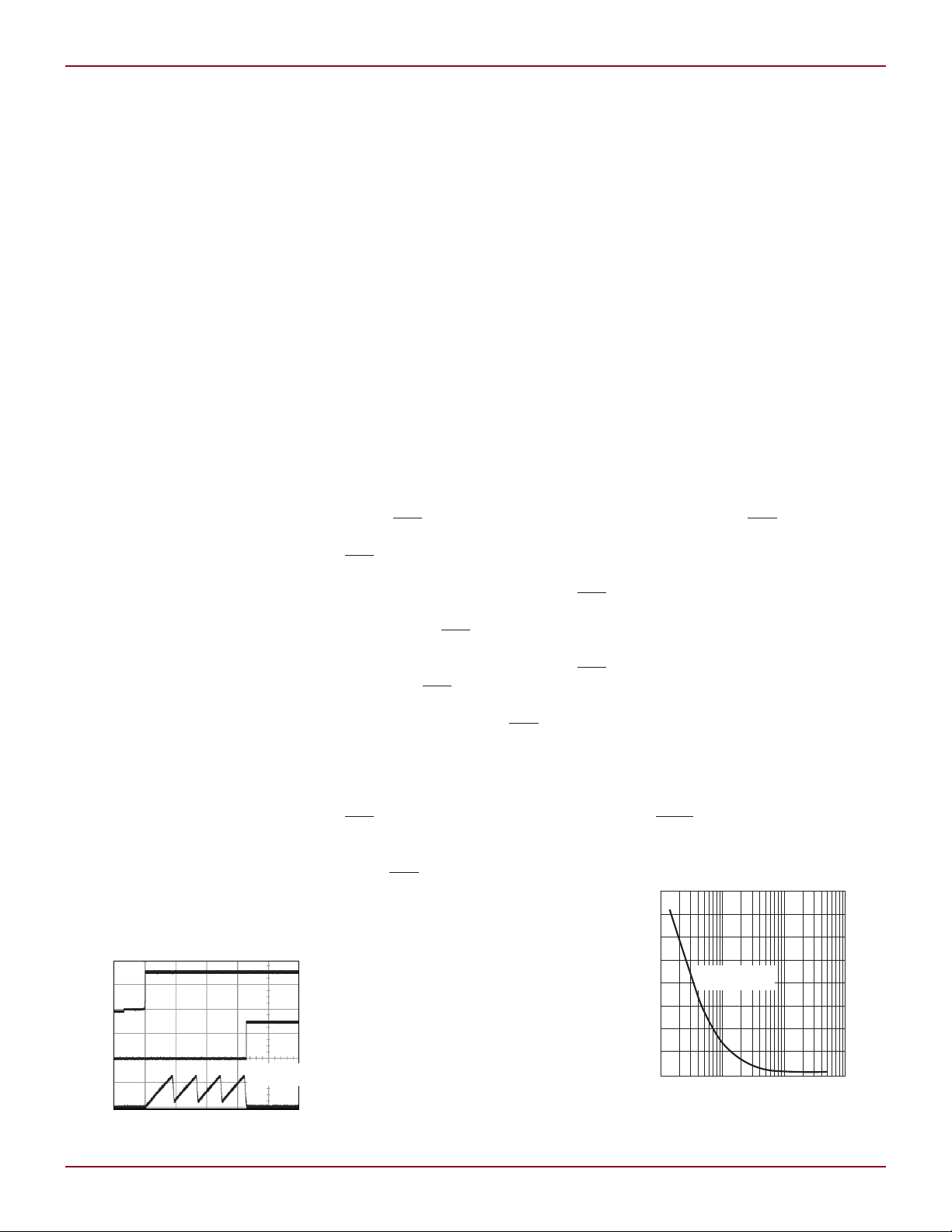
The POR comparator is designed to
avoid false triggering. High frequency
noise on the FB pin can falsely trip
RST, particularly when the monitored
output is already near the reset threshold. This can cause oscillatory behavior
at the RST pin. The traditional way of
tackling this problem is to add some
DC hysteresis in the comparator input,
which changes the threshold point
once the output flips. The problem
is that the addition of DC hysteresis
makes the trip voltage less accurate,
since the trip point changes once the
output changes. The LT3689 does not
use hysteresis. Instead, it performs an
integration-like function on transient
events at the comparator. In this way
the magnitude and duration of the
event are both important to the comparator threshold. Figure 3 illustrates
the typical transient duration versus
comparator overdrive (as a percentage
of trip threshold) required to trip the
comparator.
Selecting the Reset
Timing Capacitor
The reset timeout period is adjustable
in order to accommodate a variety of
microprocessor applications. The reset
timeout period, t
, is adjusted by
RST
connecting a capacitor between the
C
pin and ground. The value of this
POR
capacitor is determined by:
C
= t
POR
with C
• 432 • 10
RST
in Farads and t
POR
onds. The C
–9
in sec-
value per millisecond
POR
RST
of delay can also be expressed as
C
/ms = 432 (pF/ms).
POR
Leaving the C
pin unconnected
POR
generates a minimum reset timeout
of approximately 25µs with 10kΩ
pull-up to 5V on RST pin. Maximum
reset timeout is limited by the largest
available low leakage capacitor. The
accuracy of the timeout period will
be affected by capacitor leakage (the
nominal charging current is 2µA) and
capacitor tolerance. A low leakage ceramic capacitor is recommended.
Watchdog Modes:
Timeout or Window
The LT3689 also includes an adjustable watchdog timer that monitors a
microprocessor’s activity. If a code
execution error occurs in a µP, the
watchdog detects the error and sets
the WDO pin low. This signal can
be used to interrupt a routine or to
reset a µP.
Figure 3. Typical transient duration
vs POR comparator overdrive
25

L DESIGN FEATURES
t
WDU
t
WDU
t < t
WDL
t
RST
t
RST
t
RST
WATCHDOG TIMING (W/T = HIGH), TIMEOUT MODE
WDO
WDI
WDI
WDO
WATCHDOG TIMING (W/T = LOW), WINDOW MODE
t
RST
= PROGRAMMED RESET PERIOD
t
WDU
= WATCHDOG UPPER BOUNDARY PERIOD
t
WDL
= WATCHDOG WINDOW MODE LOWER BOUNDARY PERIOD
VUV = OUTPUT VOLTAGE RESET THRESHOLD
The watchdog is operated either
in timeout or window mode (refer to
Figure 4). In timeout mode, the microprocessor needs to toggle the WDI pin
before the watchdog timer expires to
keep the WDO pin high. If the voltage
on the WDI pin does not transition
during the programmed timeout period
then the circuitry pulls WDO low.
In window mode, the WDI pin’s
negative-going pulses must appear
inside a programmed time window to
prevent WDO from going low. If more
than two falling pulses are registered
in the lower boundary period (t
the WDO pin is forced low. The WDO
pin also goes low if no negative edge
is supplied to the WDI pin within the
upper boundary period (t
During a code execution error, the
microprocessor outputs WDI pulses
that are either too fast or too slow.
This condition asserts WDO low and
forces the microprocessor to reset the
program.
In window mode, the WDI signal is
bounded by an upper and lower boundary periods for normal operation. The
period of the WDI input signal should
be longer than the window mode’s lower boundary period and shorter than
the upper boundary period to keep
WDO high under normal conditions.
The window mode’s lower and upper
boundary periods have a fixed ratio
of 31. These times can be increased
or decreased by adjusting an external
capacitor on the C
In both watchdog modes, when
WDO is asserted, the reset timer is
enabled. Any WDI pulses that appear
while the reset timer is running are
ignored. When the reset timer expires,
the WDO is allowed to go back high
again. Therefore, if no input is applied
to the WDI pin then the watchdog
circuitry produces a train of pulses
on the WDO pin. The high time of
this pulse train is equal to the upper
boundary period and low time is equal
to the reset period. Also, WDO and
RST cannot be logic low simultaneously. If WDO is low and there is an
undervoltage lockout fault, RST goes
low and WDO will go high.
The WDE pin allows the user to turn
on or off the watchdog function. This
26
WDT
WDU
pin.
).
WDL
),
Figure 4. Watchdog timing diagram
feature can be used to reliably program
the connected microprocessor in the
factory. During factory programming
of the microprocessor, WDE pin can
be kept high to prevent WDO from
toggling and thus prevents WDO from
interfering with the microprocessor’s
programming procedure.
Tying the WDO and RST pins
together will generate a reset signal
when either the output voltage falls
10% below the regulation value or if
there is a watchdog error.
Selecting the Watchdog
Timing Capacitor
The watchdog upper boundary period
is adjustable and can be optimized
for software execution. The watchdog
upper boundary period is adjusted by
connecting a capacitor between the
C
pin and ground. Given a specified
WDT
watchdog upper boundary period, the
capacitor is determined by:
C
= t
WDT
• 55 (pF/ms)
WDU
The window mode lower boundary
period has a fixed relationship to upper
boundary period for a given capacitor.
The lower boundary period is related
to the upper boundary period by the
following:
t
= 1/31 • t
WDL
WDU
Leaving the C
pin unconnected
WDT
generates a minimum watchdog upper boundary period of approximately
200µs with 10kΩ pull-up to 5V on
WDO pin. Maximum timeout is limited
by the largest available low leakage
capacitor. The accuracy of the upper
and lower boundary periods is affected
by capacitor leakage (the nominal
charging current is 2µA) and capacitor tolerance. A low leakage ceramic
capacitor is recommended.
Conclusion
The wide input range, low quiescent
current, supervisory features, robustness and small size of the LT3689
makes it an ideal candidate to power
automotive and industrial applications. The part withstands 60V VIN
transients and normal operation is
guaranteed for max VIN of 36V, and
the part is robust against inrush and
short circuit conditions. The Burst
Mode circuitry provides high efficiencies at light loads. Programmable
switching frequency allows the designer to trade off between component
size and efficiency. The accurate POR
and Watchdog circuitry of LT3689
allows complete supervisory control
of a microprocessor connected to
the output of the LT3689 switching
regulator.
L
Linear Technology Magazine • March 2009
 Loading...