

advertisement
Dual Output Monolithic Synchronous Buck Regulator Operates
from 3.6V to 15V Inputs and Delivers 3A Per Channel – Design Note 1020
Tom Gross
Introduction
The LTC3633 is a high efficiency, dual output monolithic
synchronous step-down switching regulator, capable of
delivering 3A of output current per channel from input
voltages between 3.6V and 15V. Its compact 4mm × 5mm
QFN pack age has very low thermal impe dance eliminating
the need for an external heat sink. Its high input voltage
capability makes the LTC3633 ideal for 12V distributed
power systems.
1.8V and 3.3V 2MHz Buck Regulator
Figure 1 shows a LTC3633 12VIN to 1.8V
and 3.3V
OUT
OUT
3A, buck regulator. With the frequency setting pin, RT,
connected to the in ternal 3.3V regulator rail (INTVCC), this
circuit runs at 2MHz —the LTC3633 switching frequency
is programmable from 500kHz to as high as 4MHz, and
can also be synchronized to an external clock—reducing
the value and size of the output capacitors and inductor.
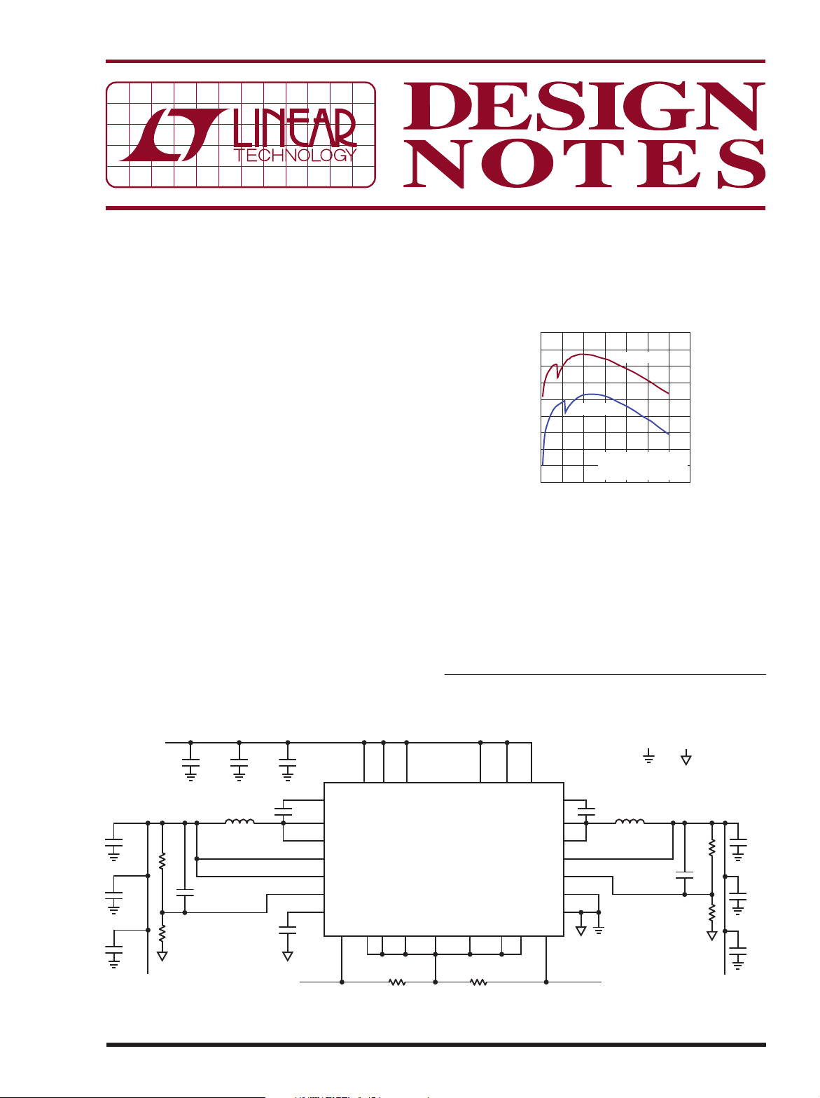
Even with this high switching frequency, the efficiency of
this circuit is good: 87% at full load for the 3.3V regulator and 82% at full load for the 1.8V regulator, at 12VIN
(see Figure 2).
94
92
90
88
86
84
EFFICIENCY (%)
82
80
78
76
,
Figure 2. High Efficiency from Each Channel for the
V
= 1.8V
OUT
0.5 3.5
0
1 1.5 2 2.5 3
LOAD CURRENT (A)
V
OUT
Burst Mode
= 3.3V
VIN = 12V
F
SW
®
OPERATION
= 2MHz
DN1020 F02
Circuit in Figure 1
By connecting the phase mode pin (PHMODE) to
INTVCC, the two internal regulators operate 180 degrees
out-of-phase with respect to each other, reducing the
input current ripple, and thus, the number and value of
input capacitors. Due to a controlled on-time design,
the LTC3633 achieves very fast load transient response
L, LT, LTC, LTM, Linear Technology, Burst Mode and the Linear logo are registered
trademarks of Linear Technology Corporation. All other trademarks are the property of
their respective owners.
3.6V TO 15V
V
IN
C
OUT1
22µF
6.3V
1206
C
OUT3
22µF
6.3V
1206
C
OUT5
10µF
6.3V
0805
V
11/10/1020
OUT1
1.8V
C
IN1
47µF
16V
PGOOD1
1210
C
BST1
0.1µF
C
4700pF
20
23
24
25
10
28
27
SS1
21 22 3 6 1615
V
IN1VIN1
BOOST1
SW1
SW1
VON1
TRACKSS2
VFB1
TRACKSS1
ITH1 RT
26 5
Figure 1. LTC3633: 1.8V
RUN1 RUN2 V
LTC3633EUFD
INTV
PHMODE MODE/SYNC V2P5 ITH2 PGOOD2PGOOD1
R
100k
PG1
OUT
CC
2 19 4 18 11 81
and 3.3V
R
100k
OUT
PG2
IN2VIN2
BOOST2
SW2
SW2
VON2
VFB2
PGND
SGND
17
C
BST2
1µF
14
13
IHLP-2020BZER1R0M01
12
9
29
7
PGOOD2
, 2MHz Buck Regulator
L2
1µH
VISHAY
POWER
GROUND
SIGNAL
GROUND
V
OUT2
C
V
OUT2
3.3V
OUT2
22µF
6.3V
1206
C
OUT4
22µF
6.3V
1206
C
OUT6
10µF
6.3V
0805
DN1020 F01
3A
R4
61.9k
1%
C
FFW2
10pF
R6
13.7k
1%
L1
1µH
VISHAY
C
IN2
47µF
16V
1210
C
IN3
22µF
16V
1206
V
OUT1
IHLP-2020BZER1R0M01
R3
20k
1%
C
FFW1
10pF
R5
10k
1%
3A
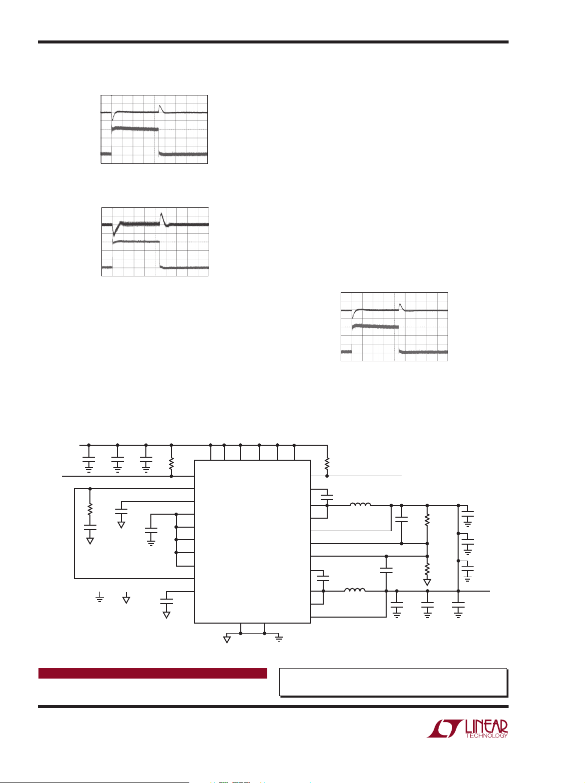
with minimal output capacitance, as shown in Figure
3. With only 50µF of output capacitance, it takes only
10µs to recover from a 3A load step that results in less
V
OUT
100mV/DIV
AC-COUPLED
I
OUT
1A/DIV
DN1020 F03a
DN1020 F03b
V
OUT
100mV/DIV
AC-COUPLED
I
OUT
1A/DIV
20µs/DIV
V
: 12VIN TO 1.8V
OUT1
3A LOAD STEP, 2MHz SWITCHING FREQUENCY
FORCED CONTINUOUS MODE,
INTERNAL COMPENSATION
V
: 12VIN TO 3.3V
OUT2
3A LOAD STEP, 2MHz SWITCHING FREQUENCY
FORCED CONTINUOUS MODE,
INTERNAL COMPENSATION
OUT
20µs/DIV
OUT
LOAD STEP
LOAD STEP
Figure 3. Load Step Responses for the Figure 1 Circuit
than 100mV of output voltage deviation. Note that compensation is internal, set up by tying the compensation
pin (ITH) to INTVCC. This connects an internal series RC
to the compensation point of the loop, eliminating the
need for external compensation components. To further
optimize the loop, an external RC circuit can be applied
to the ITH pin.
1.2V
, 6A, Out-of-Phase Supply
OUT
The LTC3633’s two internal regulators can be combined
form a single output circuit, operating out-of-phase to
deliver high total output current with minimal input and
output capacitance—useful for distributed power systems. This design also generates lower high-frequency
EMI noise than a single-phase design, due to the lower
input ripple current c aused by the out-of-p hase switching
currents with respect to each other (see Figure 4). The
12VIN to 1.2 V
dual-phase LTC3633 regulator is shown
OUT
in Figure 4, with Figure 5 showing its load step response.
Conclusion
The dual 3A output LTC3633 provides a high performance
compact regulator solution for powering low voltage
loads in 12V intermediate bus systems. Configured as a
two-phase, single output regulator, it can deliver up to
6A with minimum input ripple and an effective switching
frequency up to 8MHz.
V
OUT
100mV/DIV
AC-COUPLED
I
OUT
2A/DIV
20µs/DIV
DUAL V
: 12VIN TO 1.2V
OUT
6A LOAD STEP, 2MHz SWITCHING FREQUENCY
FORCED CONTINUOUS MODE, EXTERNAL COMPENSATION
OUT
Figure 5. Load Step Response
DN1020 F05
LOAD STEP
V
3.6V TO 15V
IN
PGOOD1
C
IN3
22µF
16V
1206
R
ITH
6.49k
1%
C
ITH
470pF
POWER
GROUND
SIGNAL
GROUND
C
IN2
47µF
16V
1210
C
4700pF
C
IN1
47µF
R
PG1
16V
100k
1210
SS1
CV
CC
1µF
C
SS2
4700pF
21 22 3 6 1615
V
IN1VIN1
1
PGOOD1
26
ITH1
27
TRACKSS1
19
INTV
CC
18
V2P5
4
MODE/SYNC
2
PHMODE
5
RT
11
ITH2
10
TRACKSS2
Figure 4. 6A Out-of-Phase Buck Regulator Using the LTC3633
Data Sheet Download
www.linear.com
Linear Technology Corporation
1630 McCarthy Blvd., Milpitas, CA 95035-7417
(408) 432-1900 ● FAX: (408) 434-0507 ● www.linear.com
RUN1 RUN2 V
SGND PGND
LTC3633EUFD
7 29
IN2VIN2
PGOOD2
BOOST1
BOOST2
SW1
SW1
VON1
VFB1
VFB2
SW2
SW2
VON2
DN1020 F04
R
PG2
100k
8
20
23
24
25
28
9
17
14
13
12
L1
C
BST1
0.47µH
0.1µF
VISHAY
IHLP-2525CZERR47M01
C
BST2
L2
0.1µF
0.47µH
VISHAY
IHLP-2525CZERR47M01
For applications help,
call (408) 432-1900, Ext. 3229
LINEAR TECHNOLOGY CORPORATION 2010
PGOOD2
V
OUT1
R1
C
FFW1
20k
10pF
1%
C
22µF
6.3V
1206
OUT2
R2
20k
1%
C
OUT4
22µF
6.3V
1206
V
OUT2
C
FFW2
10pF
dn1020f LT/TP 1110 • PRINTED IN THE USA
C
OUT6
10µF
6.3V
0805
C
22µF
6.3V
1206
C
22µF
6.3V
1206
C
10µF
6.3V
0805
OUT1
OUT3
OUT5
V
1.2V
6A
OUT
 Loading...