

L DESIGN IDEAS
POWER LOSS (mW)
EFFICIENCY (%)
LOAD CURRENT (mA)
1001
100
50
50
0
10
60
70
80
90
10
20
30
40
EFFICIENCY
POWER LOSS
V
OUT
= 5V
VIN = 24V
VIN = 10V
VIN = 10V
V
OUT
1V/DIV
V
IN
10V/DIV
50µs/DIV
V
IN
LTC3642-5
RUN
HYST
SW
V
IN
5V TO 45V
C
IN
1µF
C
OUT
10µF
V
OUT
5V
50mA
V
OUT
SS
I
SET
GND
150µH
C
IN
: TDK C3225X7R1H105KT
C
OUT
: MURATA GRM32DR71C106KA01
L1: COILCRAFT LPS6225-154ML
Robust DC/DC Step-Down Converter
in 3mm × 3mm DFN Resists 60V
Input Surges
Introduction
Industrial and test equipment must
often run on relatively unregulated
9V-to-24V rails that also support high
current and inductive load switching of
electromechanical devices. When such
devices switch on and off, momentary
power surges disrupt power flow,
causing voltage fluctuations and large
overvoltage spikes on the rail.
The LTC3631, L TC3632 and
LTC3642 are robust, monolithic DC/
DC step-down solutions that produce
a well-regulated supply even in volatile
voltage environments. All can operate
from a wide input voltage ranges and
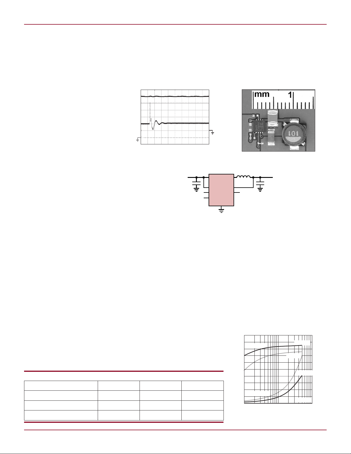
sustain repetitive 60V surges (see
Table 1). The output voltage is immune
to large voltage swings in the input
(see Figure 1).
Compact and Easy to Use
The LTC3642 comes in compact 3mm
× 3mm DFN and MS8E packages with
integrated MOSFETs, as shown in
Figure 2. It is extremely easy to use,
requiring no loop compensation. The
3.3V and 5V fixed output versions only
need two capacitors and an inductor
for operation (see Figure 3).
The constant peak switch current
thresholds of these devices inherently
protect them from output short circuits. Moreover, each of these devices
can reduce its peak switch current
threshold such that smaller input and
output capacitors can be used.
When operating with a high input
voltage source, the LTC3642’s RUN
pin can be optionally configured to
Figure 1. The LTC3642 continues to regulate
the output despite a >45V spike on the input.
Figure 3. With the LTC3642EDD-3.3/5 only two capacitors
and an inductor are required for operation
increase its undervoltage lockout
(UVLO). Until the input voltage exceeds the UVLO, the input remains
disconnected from the load. The RUN
pin can be tied directly to the input
voltage and can be used together with
the hysteresis pin to prevent unwanted
UVLO triggering due to noisy input
supplies and high voltage coupling
in harsh environments. When above
the UVLO, the LTC3642 soft starts
its output with an internal 0.75ms
timer. The duration of the soft-start
timer can be increased by adding an
Figure 2. The solution size of LTC3642-3.3/5
in a 3mm × 3mm DFN package
regulator which does not suffer significant power loss as a result of IR
drop between the input and output.
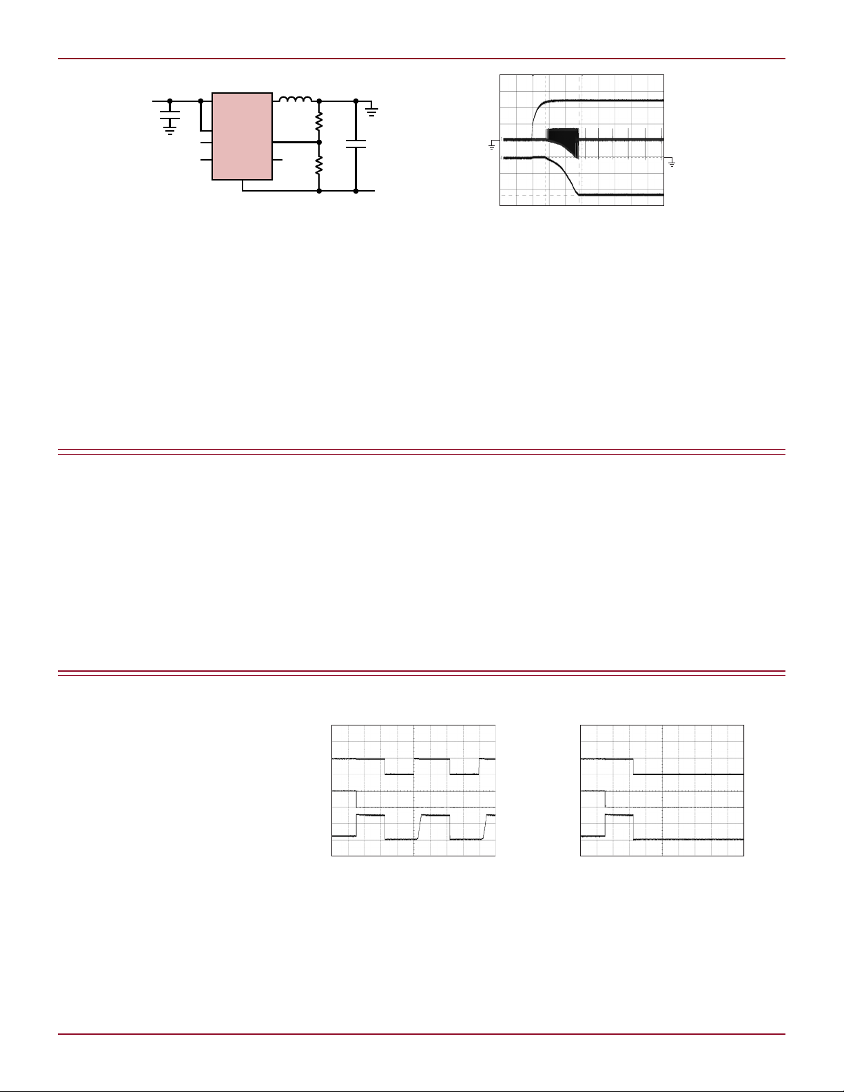
High efficiency is also achieved with
Burst Mode® operation, which reduces
switching activity at light loads to
minimize switching losses. Figure
4 shows a fairly constant efficiency
curve from light load all the way to
full load. During shutdown, this device
only draws 3µA even at a maximum
input voltage of 45V. With such high
efficiency, the LTC3642 is a good fit
in battery-operated motorized vehicles,
external capacitor in the SS pin.
High Efficiency
Unlike a linear regulator, the LTC3642
is a monolithic synchronous buck
by Chuen Ming Tan
Table 1. Comparison of monolithic wide input range buck regulators
Maximum Output Current 100mA 20mA 50mA
Input Voltage Operating Range 4.5V–45V 4.5V–50V 4.5V–45V
34
34
Input Voltage Abs Max 60V 60V 60V
LTC3631 LTC3632 LTC3642
Figure 4. Efficiency for circuit in Figure 3
Linear Technology Magazine • September 2009
DESIGN IDEAS L
V
IN
5V/DIV
V
OUT
10V/DIV
V
SW
20V/DIV
10ms/DIV
V
IN
LTC3642
RUN
C
IN
1µF
HYST
SW
V
IN
12V
V
OUT
–24V
18mA
V
FB
SS
I
SET
GND
L1
100µH
R1
1.47M
R2
49.9k
CIN: TDK C3225X7R1H105KT
C
OUT
: MURATA GRM32DR71C106KA01
L1: TYCO/COEV DQ6530-101M
C
OUT
10µF
I
OUT
FAULT
V
OUT
10ms/DIV
I
OUT
FAULT
V
OUT
10ms/DIV
Figure 5. Generating a negative 24V output
voltage from a positive 12V input voltage
portable medical instruments and
certain automotive applications.
Positive-to-Negative Converter
The LTC3642 can produce a negative
output voltage from a positive input
voltage without the use of transformers
(see Figure 5). In this configuration,
the LTC3642 actually operates in an
inverting buck-boost mode. Its wide in-
LTC6930, continued from page 23
concern, and extreme accuracy is not
paramount. Such applications include
clocking microprocessors and microcontrollers, acting as a time base for
low speed serial communication protocols such as USB and RS232, digital
audio applications, clocking switching
power supplies and anywhere a general
purpose clock is needed.
Figure 6. The LTC3642’s wide input voltage swing makes it suitable
for generating a negative output from positive input voltage.
put voltage range, up to 45V, provides
sufficient headroom to generate any
negative voltage between –0.8V and
–40.5V. Figure 6 shows LTC3642 producing a –24V output from a 12V input
supply from start-up. The LTC3642
is inherently stable in this configuration with no external compensation
components required.
Conclusion
When comparing clock power dissipation it is important to consider not just
the dissipation of the oscillator itself,
but also how the oscillator’s features
and start-up times effect the dissipation of the entire system. Crystal
oscillators not only dissipate more current than other solutions, but can have
Conclusion
The LTC3642, LTC3631 and LTC3632
are a rugged DC/DC converters for use
in applications where a stable voltage
output must be produced from poorly
regulated high voltage rails. Their
compact size and high efficiency make
them easy to use in a wide variety of low
power applications, including mobile
and battery powered devices.
other start-up and control characteristics that lead to power waste. When
the LTC6930’s on-the-fly frequency
programmability and one-clock-cycle
settling time are considered, it is clear
that it conserves much more system
power than its dissipation specification
would indicate
L
L
LTC3529, continued from page 33
on a pin-selectable setting, the IC can
be configured to either periodically
attempt to power up (RST pin high,
Figure 4a), or remain shut down until power is cycled to the device (RST
pin low, Figure 4b). The waveform
indicating the fault condition is seen
at the Fault pin and is produced by
an internal open-drain device whose
input is pulled high in the event of
a fault. The Fault pin can either be
connected to a microprocessor or
drive an LED.
Conclusion
High conversion efficiency and the
ability to detect and handle output
shorts make the LTC3529 an ideal so-
Linear Technology Magazine • September 2009
4a. RST high: converter attempts power-up
every 15ms.
Figure 4. A fault detection mechanism powers down
the converter, providing robustness to output shorts
lution for either peer-to-peer portable
applications or point-of-load board
power with robust fault handling.
The 1.5MHz switching frequency
4b. RST low: converter remains shut down
until power is cycled.
and highly integrated design of the
LTC3529 yield compact solutions with
minimal design effort.
L
3535
 Loading...