

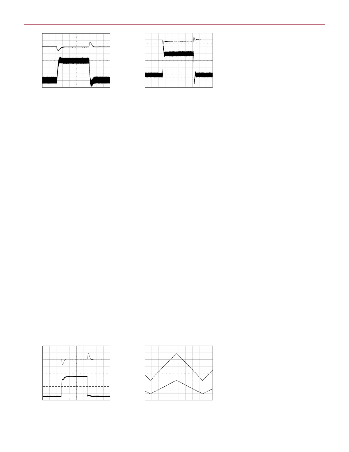
LOAD CURRENT (mA)
1
10010 1k
EFFICIENCY (%)
10k
0
10
20
30
40
50
60
70
80
90
100
BURST MODE OPERATION
PULSE SKIPPING MODE
FORCED CONTINUOUS
MODE
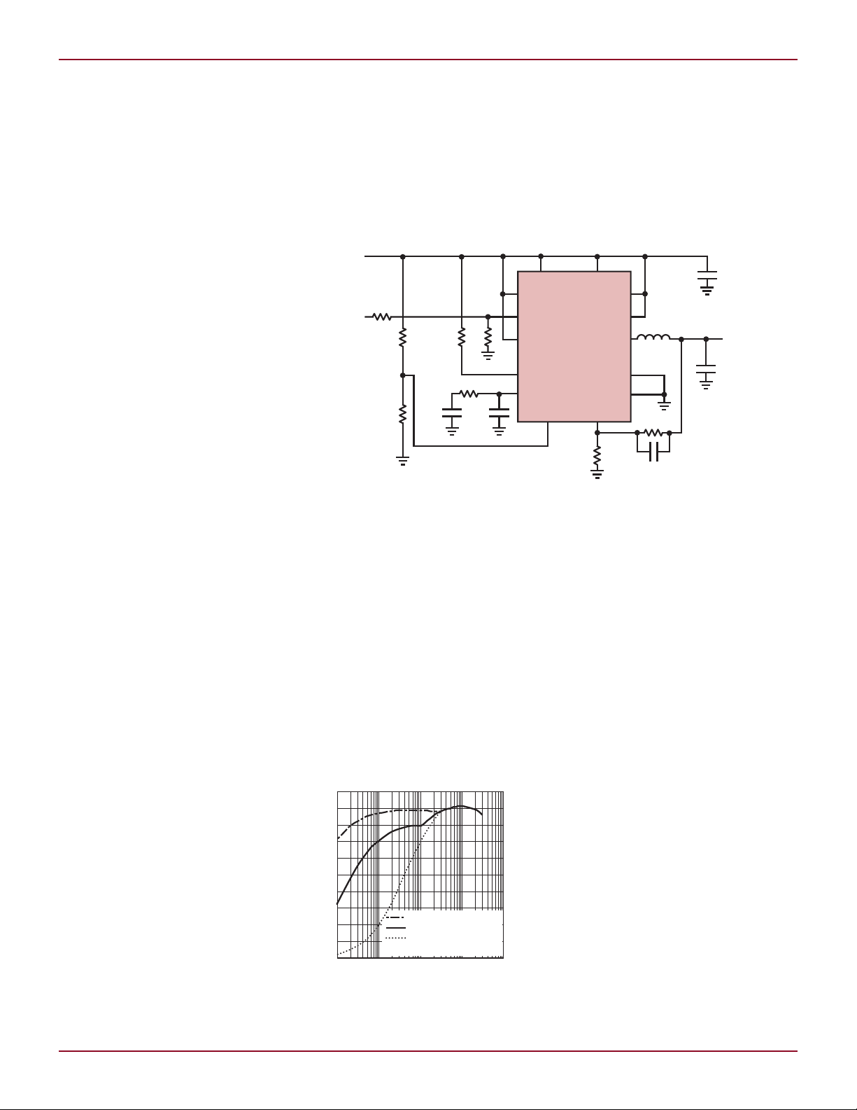
LT3612
PWN_DRIVER
DDR
SVIN PVIN
MODE VFB
RUN
TRACKSS
RT_SYNC
PGOOD
ITH
SW
SGROUND
PGROUND
VTT=VDD/2
1.25V
±1.5A
22pF
110k
470pF 10pF
12.1k
100k
402k
V
IN
3.3V
V
DD
2.5V
100k
1M
165k
L1
470nH
33µF
=2
22µF
=2
1M
L DESIGN FEATURES
Monolithic Synchronous Step-Down
Regulator Sources 3A or Sinks 1.5A
in TSSOP or 3mm × 4mm QFN
by Genesia Bertelle
Introduction
The LTC3612 monolithic synchronous
buck regulator can source 3A and
sink 1.5A from a tiny 3mm × 4mm
QFN or 20-lead TSSOP package with
exposed pads for improved thermal
performance. This device saves space,
minimizes external components and is
highly efficient. It employs a constant
frequency, current mode architecture
that operates from an input range of
2.25V to 5.5V—suitable for a single
Li-Ion battery or low voltage input
applications. The LTC3612 provides
an adjustable regulated output down
to 0.6V.
The LTC3612 uses Burst Mode®
operation to increase efficiency at light
loads, consuming less than 100µA of
supply current at no load. Adjustable
compensation allows the transient
response to be optimized over a wide
range of loads and output capacitors.
The internal synchronous switch
increases efficiency and eliminates
the need for an external catch diode,
saving external components and board
space.
Design Versatility
Depending on the application requirements, a designer can either prioritize
light load efficiency or minimize supply noise by choosing from three light
load operating modes: Burst Mode
operation, pulse-skipping, or forced
continuous modes. Burst Mode operation provides high efficiency over
the entire load range by reducing gate
charge losses at light loads. Burst
Mode operation is an efficient solution
for low current applications, but in
some applications noise suppression
is a higher priority. Forced continuous
operation, though not as efficient as
Burst Mode operation at light loads,
maintains a constant switching frequency, making it easier to reduce
10
Figure 1. High efficiency and very compact 1.5A LTC3612 VTT power supply with 3.3V input
noise and RF interference. In forced
continuous operation, the LTC3612
can source and sink current. Pulseskipping mode is similar to Burst Mode
operation. It reduces output voltage
ripple, but incurs more gate charge
losses, compromising light load efficiency. Although not as efficient as
Burst Mode operation at low currents,
pulse-skipping mode still provides
high efficiency for moderate loads.
The default frequency of 2.25MHz is
chosen by tying the RT/SYNC pin to
VIN. This high frequency allows the use
of tiny inductors and ceramic output
capacitors without compromising efficiency. The switching frequency can
be set from 300kHz to 4MHz with an
external resistor or synchronized to
an external clock, where each switching cycle begins at the falling edge of
the external clock signal. All operating modes (Burst Mode operation,
pulse-skipping and forced continuous
mode) can be selected in combination
with the default 2.25MHz frequency,
a frequency defined by an external
resistor or synchronization with external clock.
The LTC3612 offers a power good
indicator (PGOOD pin), which monitors the output voltage. The PGOOD
pin is an open-drain output which is
pulled down to ground during shut
down, start-up and while the output
voltage is outside the power good
voltage window (±7.5% of the final
programmed output voltage). If the
output voltage stays inside the power
good window for more than 100µs, the
PGOOD pin is released. If the output
Figure 2. Efficiency vs load current, 2.25MHz
switching frequency, in various operating
modes
voltage remains outside the power
good window for more than 100µs,
the PGOOD pin is pulled down.
The 100% duty cycle capability for
low dropout conditions allows maxi-
Linear Technology Magazine • December 2009
V
DD
100mV/DIV
V
TT
100mV/DIV
1ms/DIV
V
OUT
200mV/DIV
I
LOAD
1A/DIV
0A
50µs/DIV
–1.5V
1.5V
V
OUT
200mV/DIV
I
L
1A/DIV
50µs/DIV
V
OUT
= 1.8V
I
LOAD
= 100mA TO 3A
V
MODE
= 1.5V
V
OUT
100mV/DIV
I
L
1A/DIV
50µs/DIV
V
OUT
= 1.8V
I
LOAD
= 100mA TO 3A
V
MODE
= 1.5V
V
ITH
= V
IN
Figure 3. Load step transient in forced continuous mode
mum energy to be extracted from a
Li-Ion battery. In dropout, the output
voltage is determined by the input
voltage minus the voltage drop across
the internal P-channel MOSFET (only
70mΩ) and the inductor resistance.
Power Supply Tracking and
DDR Applications
The LTC3612 supports coincidental or
ratiometric ramp-up and ramp-down
tracking of another supply via the
TRACK/SS pin. For TRACK/SS voltages lower than 0.2V, the switching
frequency is reduced to ensure that
the minimum duty cycle limit does
not prevent the output voltage from
following the TRACK/SS pin.
Start-up behavior can be programmed in one of three ways via the
TRACK/SS pin. Tying TRACK/SS to
SVIN selects the internal soft-start
circuit (1ms ramp time). Alternately,
external soft-start timing can be programmed with a TRACK/SS capacitor
to ground and a resistor to SVIN. Finally, the TRACK/SS pin can be used to
force the LTC3612 to track the start-up
behavior of another supply.
When running in DDR mode, the
TRACK/SS pin can be used as an
external reference input, allowing the
Figure 4. Load transient response for ±1.5A
load applied to the circuit shown in Figure 1
Linear Technology Magazine • December 2009
DESIGN FEATURES L
LTC3612 to power DDR memory. In
this mode, the power good window
moves in relation to the actual TRACK/
SS pin voltage.
Typically DDR memory needs at
least two main power supplies: V
and VTT, where V
the V
supply with VTT = V
DD
must always track
TT
Since the termination resistors can
carry current in either direction, the
V
power supply must be able to both
TT
source and sink current while tracking
the V
supply.
DD
Two LTC3612 converters can be
used to generate both V
and V
DD
as shown in the circuit in Figure 1.
V
voltages range from 1.25V down
TT
to 0.75V for different DDR standards.
LTC3612 can be used for all DDR
standards because the TRACK/SS
voltage can accept a reference voltage
from 0.6V down to 0.3V (although
TRACK/SS voltage values from 0.4V
to 0.5V are the most accurate).
Optional AVP Mode with
Internal Compensation
Fast load current transient response is
an important feature in microprocessor power supplies. Normally, several
capacitors in parallel are required to
meet microprocessor transient re-
Figure 5. VTT responding to a change in VDD
for the circuit shown in Figure 1
DD
DD
/2.
,
TT
quirements, where capacitor ESR and
ESL primarily determine the amount
of droop or overshoot in the output
voltage. If a load step with very fast
slew rate occurs, an output voltage
excursion is seen for transients in
both directions: that is for full load to
minimum load and for the minimum
load to full load.
If the ITH pin is tied to SVIN, the active voltage positioning (AVP) mode and
internal compensation are selected.
AVP mode intentionally compromises
output voltage regulation by reducing
the gain of the feedback circuit, resulting in an output voltage that varies
with load current.
When the load current suddenly
increases, the output voltage starts
from a level slightly higher than nominal so the output voltage can droop
and stay within the specified voltage
range. When the load current suddenly
decreases the output voltage starts
at a level lower than nominal so the
output voltage can overshoot and stay
within the specified voltage range. In
AVP mode the external compensation
at ITH pin is not needed, reducing
external components.
Short-Circuit Protection
The LTC3612 is protected against
an output short to ground. When
the output is shorted to ground, the
inductor current decays very slowly
during a single switching cycle. The
LTC3612 uses two techniques to prevent inductor current runaway from
occurring.
First, if the output voltage drops below 50% of its nominal value, the peak
current clamp is decreased, reducing
the maximum inductor current. When
the output voltage reaches 0V, the
clamp voltage at the ITH pin drops to
40% of the clamp voltage during normal operation. The short-circuit peak
inductor current is determined by the
minimum on-time of the LTC3612, the
input voltage and the inductor value.
This foldback behavior helps in limiting the peak inductor current when the
output is shorted to ground.
Secondly, a limit is also imposed
on the valley inductor current. If the
continued on page 15
11

DESIGN FEATURES L
V V V
V
V
BAT PRE BAT MIN BAT FLOAT( ) ( ) ( )
•
.
.
< =
2 3
3 3
V V V
V
V
BAT PRE BAT MIN BAT FLOAT( ) ( ) ( )
•
.
.
< =
2 3
3 3
∆ •
• ∆
•
( )
V
V
R
R R
R R
IN NTC
REGINNTC NTC
IN NTC
=
2 1
mode and maximum charge current
is determined as follows:
V
BAT(MIN)
V
BAT(PRE)
V
CHRG(PRE)
V
CHRG(PRE)
= 5.7V
< 5.7V
= 0.15 • I
= 0.3A
CHRG
Using and efficiency of 0.85, plot PIN
over the range of VIN that is current
controlled. This is the regulated VIN,
or V
of the V
, power line. The intersection
REG
power line with the solar
REG
panel power curve is the operating
point. As the battery charges, the
slope of the V
power line increases,
REG
indicating the increase in input power
required to support the increasing
output power. The intersection of the
V
power line continues to follow
REG
up the solar panel’s power curves
until the charger exits constant cur rent mode.
The resulting plots are shown in
Figure 4.
The Circuit in Action
Figure 4 shows the power output of the
solar panel plotted at light intensity
levels from 100W/m2 to 1000W/m2
in 100W/m2 steps. At maximum light
intensity (top curve in Figure 4) and
the battery voltage just above the preconditioning level (V
BAT(MIN)
solar panel is producing more power
than the charger needs. The solar
panel voltage rises above the V
control voltage and travels across the
constant power line until it intersects
the light-power-intensity curve for
that intensity level (point A in Figure
4). As the battery charges, the input
power increases and the solar panel
operating point moves up the lightpower-intensity curve until the battery
at 2A), the
REG
approaches full charge (point B). The
LT3652 transitions from constant current mode to constant voltage mode
and the charging current is reduced.
The solar panel operating point moves
back down the light-power-intensity
curve to the open circuit voltage (point
C) when the battery reaches its final
float voltage.
During the charging of the battery, if
the light intensity diminishes, the operation point moves across a constant
The input voltage regulation
loop of the LT3652 has
the ability to seek out the
maximum power operating
point of a solar panel’s
power characteristic, thus
utilizing the full capacity of
the solar panel.
power line for the battery voltage until
it reaches the new power-intensity
curve. If the light intensity level continues to diminish, the operating point
travels along this constant power line
until it reaches the V
At this point the charging current is
reduced until the operating point is at
the intersection of the light-power-intensity curve and the V
(point D for constant current charging
at V
BAT(FLOAT)
with 800W/m2 illumination). As the battery continues to
charge at this light intensity level, the
operating point moves along the new
light-power-intensity curve until the
battery approaches full charge.
As darkness approaches, the operating point moves down the V
power line until charging current
ceases (point E) and the solar panel
output voltage drops below the SHDN
power line.
REG
power line
REG
REG
falling threshold at which point the
LT3652 turns off.
The remaining elements of the
design, selection of output inductor,
catch rectifier and timer capacitor,
are outlined in the design procedure
in the LT3652 datasheet along with
PCB layout considerations.
The maximum power voltage, for
a monocrystalline solar cell, has a
temperature coefficient of –0.37%/K
while the maximum power level is
–0.47%/K. This may be compensated
for by letting R
be a combination
IN1
of a series resistor and a series NTC
thermistor. The ratio of the two elements that comprise R
of R
need to be adjusted to achieve
IN2
and the value
IN1
the correct negative temperature of
VIN while still maintaining the control
range of VIN.
Conclusion
The input voltage regulation loop of
the LT3652 has the ability to seek out
the maximum power operating point
of a solar panel’s power characteristic,
thus utilizing the full capacity of the
solar panel. The float voltage regulation loop and its adjustable charging
current enable the LT3652 to be used
with many battery chemistries, making
it a versatile battery charger. The added
features of a wide input voltage range,
an auto-recharge cycle to maintain a
fully charged battery, a battery preconditioning mode, NTC temperature
sensing, selectable C/10 or timed
charging termination, a FAULT and
a charging status pins fills out the
full feature set of the LT3652. The
LT3652 is available in a 3mm × 3mm
12-lead plastic DFN, package with an
exposed pad.
L
LTC3612, continued from page 11
inductor current measured through
the bottom MOSFET increases beyond
6A, the top power MOSFET is held off
and switching cycles are skipped until
the inductor current is reduced.
Linear Technology Magazine • December 2009
Conclusion
The LTC3612 is well suited for a wide
range of low voltage step-down converter applications, including DDR
memory termination applications
requiring ±1.5A of output current. Its
high switching frequency and internal
low R
power switches allow the
DS(ON)
LTC3612 to offer a compact, high efficiency design solution supplying up
to 3A output current.
L
15
 Loading...