

L DESIGN IDEAS
V
OUT
1.2V
8A
C
OUT
100µF
s2
L1
0.5µH
V
IN
5V TO 18V
C
IN
10µF
25V
3s
+
C1
0.22µF
C
SS
0.1µF
4.7µF
6.3V
V
IN
0.47µF
25V
7.68k
1%
1500pF
R
ON
187k
1%
30.1k
1%
30.1k
1%
100k
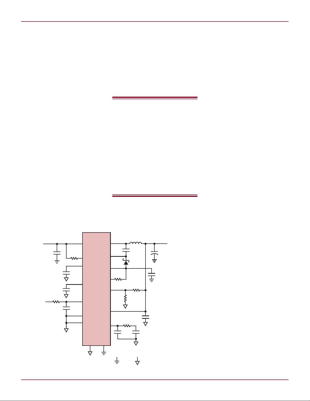
LTC3608
V
FB
I
ON
FCB
I
TH
V
RNG
PGOOD
SGND
BOOST
RUN/SS
V
ON
INTV
CC
SW
PV
IN
0.1µF
100pF
CMDSH-3
1Ω
KEEP POWER GROUND AND SIGNAL GROUND SEPARATE.
CONNECT AT ONE POINT.
= SGND
= PGND
PGND
SV
IN
0.01µF
EXTV
CC
C1: TAIYO YUDEN JMK316BJ226ML-T
CIN: TAIYO YUDEN TMK432BJ106MM
C
OUT
: TDK C4532X5R107M
L1: SUMIDA CDEP85NP-R50MC-125
32V
with Integrated FETs Deliver up to 12A
from Sub-1mm Height Packages
Introduction
Monolithic buck regulators are easy
to hook up and they make it possible
to squeeze an entire DC/DC converter
into very tight spaces. Although monolithics are an easy fit, they aren’t the
perfect fit for every application. For
instance, they typically lack the capability to efficiently convert high input
voltages (>12V) to low voltages at high
output currents (>4A), thus leaving the
job to a traditional controller IC and
external MOSFETs.
A new family of devices, though,
offers the advantages of monolithics
with the low duty cycle and high efficiency of discrete components. The
LTC3608, LTC3609, LTC3610 and
LTC3611 are synchronous buck converters that bring high power density
and simplified design to point-of-load
applications. With a maximum input of
32
32
Synchronous Buck Regulators
IN
by Stephanie Dai and Theo Phillips
are packaged in thermally enhanced
packages less than 1mm in height. A
typical application of the LTC3608 is
shown in Figure 1.
Features
The LTC3608, LTC3609, LTC3610 and
LTC3611 integrate high performance
synchronous buck controllers with
super-low R
to produce compact high efficiency
converters (Figure 2). Two package
sizes are available, each having a
high voltage or high current option
(Table 1). Each device features a sub100ns on-time, allowing very low duty
cycle operation and high switching
frequency. The current-mode control
architecture of these parts simplifies
tuning of loop stability and allows
excellent transient response with a
variety of output capacitor types, including all-ceramic output capacitor
applications.
The LTC3610 can operate in forced
continuous mode, which provides the
lowest possible output ripple and EMI,
or discontinuous mode, which has
better light load efficiency because
inductor current is not allowed to
reverse.
Current into the ION pin sets the
on-time—a resistor RON from VIN to the
ION pin reduces on-time as V
thus limiting changes in switching
frequency. Furthermore, response to a
load step can be very fast since the loop
does not have to wait for an oscillator
pulse before the top switch is turned
on and current begins increasing.
The current limit, which is inferred
from the maximum allowable sense
voltage across the on-resistance of
the bottom FET, can be adjusted by
applying a voltage to the V
Maximum load current limits for each Figure 1. Typical application of the LTC3608
Linear Technology Magazine • September 2008
DS(ON)
A new family of devices
offers the advantages of
monolithic DC/DC converters
with the low duty cycle and
high efficiency of discrete
components. The LTC3608,
LTC3609, LTC3610 and
LTC3611 are synchronous
buck converters that bring
high power density and
simplified design to point-of-
load applications.
32V they utilize current-mode control
up to a 2MHz switching frequency,
deliver up to 12A of load current, and
DMOS MOSFETs
rises,
IN
pin.
RNG
part are shown in Table 1. Soft-start
LOAD STEP 1A-8A
VIN = 12V
V
OUT
= 1.2V
FCB = 0V
200mV
V
OUT
200mV/DIV
I
L
5A/DIV
LOAD CURRENT (A)
0.01
50
EFFICIENCY (%)
55
65
75
60
70
80
85
90
0.1 1 10
VIN = 12V
FREQ = 550kHz
CCMDCM
and latch off functions are controlled
by the RUN/SS pin, preventing inrush
current and current overshoot during
startup, and providing the option of
latch-off if an under voltage or short
circuit is presented. An open drain
power-good pin monitors the output
and pulls low if the output voltage is
±10% from the regulation point.
Conclusion
The LTC3608, LTC3609, LTC3610
and LTC3611 buck regulators offer the efficiency and power output
capability of separate (controller +
discrete) MOSFET solutions with
the ease-of-use and space-saving
advantages of traditional MOSFETon-the-die monolithics. These parts
also yield higher efficiencies than
Figure 3. Transient response for the typical
LTC3608 application represented in Figure 1
with a load step of 1A to 8A
traditional monolithic solutions.
They conserve power, save space, and
simplify power designs. They reduce
discrete components over controller-based solutions, making them a
DESIGN IDEAS L
Figure 2. Efficiencies for a typical
LTC3608 application in discontinuous
conduction mode (DCM) and continuous
conduction mode (CCM)
good fit in everything from low power
portable device applications such as
notebook and palmtop computers
to high-power industrial distributed
power systems.
L
LTC3610 LTC3611 LTC3608 LTC3609
PVIN Max 24V 32V 18V 32V
I
Max 12A 10A 8A 6A
LOAD
Package
R
DS(ON)
Top FET
R
DS(ON)
Bottom FET
LTC4009, continued from page 20
9mm × 9mm × 0.9mm
64-pin
12mΩ 15mΩ 14mΩ 19mΩ
6.5mΩ 9mΩ 8mΩ 12mΩ
LTC4009 family monitors the voltage
across the input blocking diode for
unexpected voltage reversal. Initial
startup, restarts from fault conditions,
and charge current reduction during
input current limit are also carefully
controlled to avoid producing reverse
current.
All members of the family provide
an input current limit flag to tell the
system when the adapter is running
at over 95% of its current capacity.
Finally, each IC features internal
over-temperature protection to prevent silicon damage during elevated
thermal operation.
Recovery from all fault conditions is
under full control of the analog feed-
Linear Technology Magazine • September 2008
Table 1. Integrated MOSFET buck regulators
9mm × 9mm × 0.9mm
64-pin
7mm × 8mm × 0.9mm
52-pin
back loops, which guarantees charging
remains suspended until the internal
feedback loops respond coherently and
report the need to supply current to
the load to maintain proper voltage or
current regulation.
Conclusion
The LTC4009 family integrates a full
set of charger building blocks in a small
PCB footprint. The result is a high
power battery charger IC with high
precision and a full set of monitoring
and fault handling features.
The LTC4009 provides adjustable
output voltage control with a simple,
external, user-programmed resistive
voltage divider. As such, it is suitable as
a general purpose charger that works
7mm × 8mm × 0.9mm
52-pin
with multiple battery chemistries and
supercaps. It offers direct control over
the entire charge process, facilitating
implementation of a wide range of
charge termination algorithms with
an external microprocessor.
The LTC4009-1 and LTC4009-2
feature pin-programmable output
voltage for common lithium-ion or
lithium-polymer battery pack configurations with one to four series cells.
For these chemistries, the number of
precision external application components is reduced without sacrificing
accuracy. Both 4.1V/cell (LTC4009-1)
and 4.2V/cell (LTC4009-2) options are
available, allowing the user to balance
capacity and safety per the demands
of the application.
L
3333
 Loading...