

15VIN, 4MHz Monolithic Synchronous Buck Regulator Delivers
5A in 4mm × 4mm QFN – Design Note 467
Tom Gross
Introduction
The LTC®3 6 0 5 i s a h i g h e f fi ciency, monolithic synchronous
step-dow n switching regulator that is cap able of delivering
5A of continuous output current from input voltages of
4V to 15V. Its compact 4mm × 4mm QFN package has
very low thermal impedance from the IC junction to the
PCB, such that the regulator can deliver maximum power
without the need of a heat sink. A single LTC3605 circuit
can power a 1.2V microprocessor directly from a 12V
rail—no need for an intermediate voltage rail.
The LTC3605 employs a unique controlled on-time/constant frequency curr ent mode architecture, making it ideal
for low duty cycle applications and high frequency operation. There are two phase-lock loops inside the LTC3605:
one servos the regulator on-time to track the internal
oscillator frequency, which is determined by an external
timing resistor, and the other ser vos the internal oscillator
to an external clock signal if the part is synchronized. Due
to the controlled on -time design, the LTC3605 c an achieve
very fast load transient response while minimizing the
number and value of external output capacitors.
The LTC3605’s switching frequency is pro grammable from
800kHz to 4MHz, or the regulator can be synchronized to
an external clock for noise-sensitive applications.
Furthermore, multiple LTC3605s can be used in parallel
to increase the available output current. The LTC3605
R5
100k
12V
V
IN
C1
22μF
16V
R3
10Ω
C6
0.1μF
25V
PGOOD
PV
IN
C2
PV
IN
22μF
16V
SV
IN
RUN
CLKIN
CLKOUT
RT TRACK MODE SGND PGND
R4
71.5k
PHMODE
C9
0.1μF
ITH INTV
LTC3605
produces an out-of-phase clock signal so that parallel
devices can be interleaved to reduce input and output
®
current ripple. A multiphase, or PolyPhase
, design
also generates lower high frequency EMI noise than a
single-phase design, due to the lower switching currents
of each phase. This confi guration also helps with the
thermal design issues normally associated with a single
high output current device.
1.8V
, 2.25MHz Buck Regulator
OUT
The LTC3605 is specifi cally designed for high effi ciency
at low duty cycles such as 12V
-to-1.8V
IN
at 5A, as
OUT
shown in Figure 1. High ef fi ciency is achieved with a low
R
a 70mΩ R
b o t t o m s y n c h r o n o u s M O S F E T s w i t c h ( 3 5 m Ω ) a n d
DS(ON)
top synchronous MOSFET switch.
DS(ON)
This circuit runs at 2.25MHz, which reduces the value and
size of the output capacitors and inductor. Even with the
high switching frequency, the effi ciency of this circuit is
about 80% at full load.
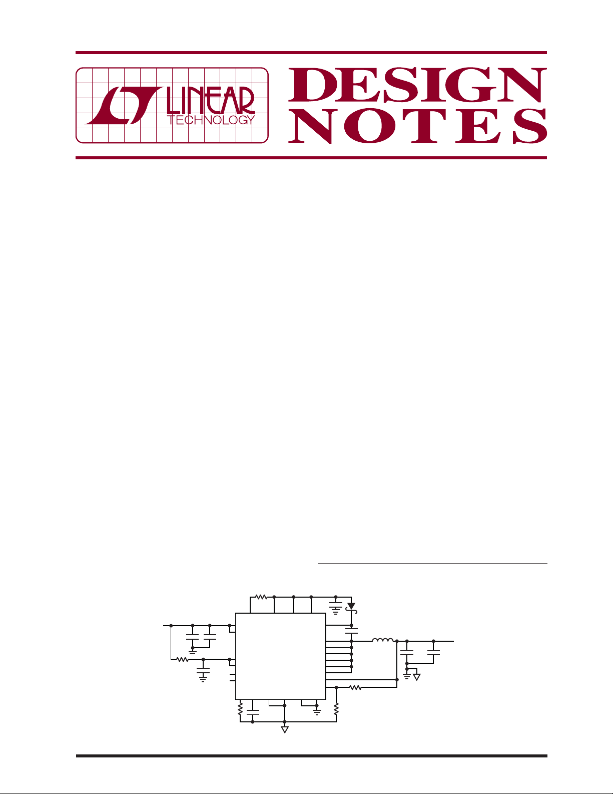
Figure 2 shows the fast load transient response of the
application circuit shown in Figure 1. It takes only 10μs
to recover from a 4A load step with less than 100mV
of output voltage deviation and only two 47μF ceramic
output capacitors. Note that compensation is internal, set
up by tying the compensation pin (ITH) to the internal
L, LT, LTC, LTM, PolyPhase, Linear Technology and the Linear logo are registered
trademarks of Linear Technology Corporation. All other trademarks are the property of
their respective owners.
2.2μF
CC
BOOST
SW
SW
SW
SW
SW
SW
V
PGND
C7
ON
FB
R1
10.0k
DN467 F01
R2
20.0k
D1
C5
0.1μF
25V
L1
0.33μH
C3
47μF
6.3V
C4
47μF
6.3V
V
1.8V
5A
OUT
06/09/467
Figure 1. 12V to 1.8V at 5A Buck Converter Operating at 2.25MHz
ΔV
O
100mV/DIV
I
O
2A/DIV
20μs/DIV
DN467 F02
Figure 2. Load Step Response of the Circuit in Figure 1
3.3V regulator rail (INTVCC). This connects an internal
series RC to the compensation point of the loop, while
introducing active voltage positioning to the output
voltage: 1.5% at no load and –1.5% at full load. The
hassle of using external components for compensation
is eliminated. If one wants to further optimize the loop,
and remove voltage positioning, an external RC fi lter can
be applied to the ITH pin.
1.2V
, 10A, Dual-Phase Supply
OUT
Several LTC3605 circuits can run in parallel and out of
phase to deliver high total output current with a minimal
amount of input and output capacitance—useful for
distributed power systems.
The 1.2V
dual-phase LTC3605 regulator shown in
OUT
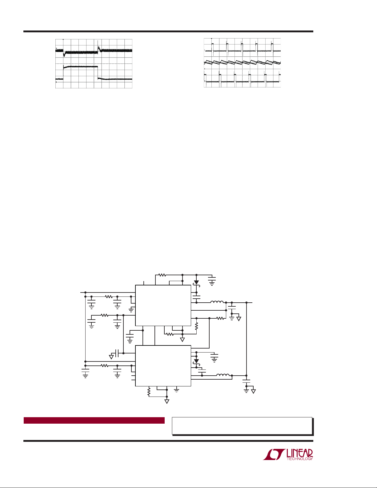
Figure 4 can suppor t 10A of outpu t current. Figure 3 shows
the 180° out-of-phase op eration of the two LTC3605s. T he
LTC3605 requires no external clock device to operate up
to 12 devices synchronized out of phase—the CLKOUT
and CLKIN pins of the devices are simply cascaded,
V
SW1
10V/DIV
DN467 F03
I
L2
5A/DIV
5A/DIV
V
SW2
10V/DIV
I
L1
500ns/DIV
Figure 3. Multiphase Operation Waveforms of the
Circuit in Figure 4. The Switch Voltage and Inductor
Ripple Currents Operate 180° Out of Phase with
Respect to Each Other
where each slave’s CLKIN pin takes the CLKOUT signal
of its respective master. To produce the required phase
offsets, simply set the voltage level on the PHMODE pin
of each device to INTV
, SGND or INTVCC/2 for 180°,
CC
120° or 90° out-of-phase signals, respectively, at the
CLKOUT pin.
Conclusion
The LTC3605 offers a compact, monolithic, regulator solution for high current applications. Due to its
PolyPhase c apability, up to 12 LTC3605s can run in par allel
to produce 60A of output current. PolyPhase operation
can also be used in multiple output applications to lower
the amount of input ripple curr ent, reducing the necessar y
input capacitance. This feature, plus its ability to operate
at input voltages as high as 15V, make the LTC3605 an
ideal part for distributed power systems.
V
IN
12V
C
22μF
C
IN1
22μF
R
8k
C
ITH
390pF
R
IN2
FILT2
10Ω
C
R
ITH
FILT1
10Ω
10pF
FILT1
0.1μF
C
C1
C
C2
10pF
C
FILT2
0.1μF
Figure 4. 12V to 1.2V at 10A 2-Phase Buck Converter
Data Sheet Download
www.linear.com
Linear Technology Corporation
1630 McCarthy Blvd., Milpitas, CA 95035-7417
(408) 432-1900
●
FAX: (408) 434-0507 ● www.linear.com
R
PG
CLKIN
PV
SV
RUN
PGND
ITH
TRACK CLKOUT RT MODE SGND
C
SS
0.1μF
TRACK CLKIN
ITH
PV
SV
RUN
PGOOD
CLKOUT
162k
100k
PGOOD
IN
IN
IN
IN
R
T2
PHMODE INTV
LTC3605
LTC3605
RT MODE SGND PGND
R
162k
T1
CC
BOOST
VON
PHMODE
INTV
BOOST
V
C
INTVCC1
2.2μF
D
BST1
L1
C
BST1
0.33μH
0.1μF
SW
FB
10.0k
FB
CC
SW
ON
R
R
FB2
FB1
10.0k
C
INTVCC2
2.2μF
D
BST2
L2
C
BST2
0.33μH
0.1μF
DN467 F04
C
OUT1
47μF
C
47μF
V
1.2V
10A
OUT2
OUT
For applications help,
call (408) 432-1900, Ext. 3229
dn467 LT/TP 0609 155K • PRINTED IN THE USA
© LINEAR TECHNOLOGY CORPORATION 2009
 Loading...