

L DESIGN FEATURES
L1
15µH
L4
10µH
I
FB3
EN/SS3
EN/SS1
FLT
SW2 GND FB2
CAP1
FB1
V
OUT1
LT3587
V
FB3VOUT3
CAP3 SW3 V
IN
SW1
C6
1µF
C1
10µF
C
FB1
2.7pF
R
FB1
1M
CCD POSITIVE
15V
50mA
V
VIN
2.5V TO 6V
C2
2.2µF
L2
15µH
L3
15µH
R
FB2
1M
CCD NEGATIVE
–8V
100mA
LED DRIVER
20mA UP TO 24V
V
VIN
2.5V TO 6V
C7
22µF
D
S2
D
S3
C4
2.2µF
R
VFB3
1.65M
(OPTIONAL)
D
S1
R
IFB3
8.06k
C5
100nF
C3
100nF
C1: MURATA GRM21BR61C106KE15L
C2: MURATA GRM188R61C225KE15D
C3, C5: MURATA GRM033R60J104KE19D
C4: MURATA GRM21BR71E225KA73L
C6: MURATA GRM155R61A105KE15D
C7: TAIYO YUDEN LMK212BJ226MG-T
C
FB1
: MURATA GRM1555C1H2R7BZ01D
C
FB2
: MURATA GRM1555C1H6R8BZ01D
L1, L2, L3: SUMIDA CDRH2D18/HP-150N
L4: TOKO 1071AS-100M
DS1, DS2, DS3: IR IR05H40CSPTR
C
FB2
6.8pF
±32V Triple-Output Supply for LCDs,
CCDs and LEDs Includes Fault
Protection in a 3mm × 3mm QFN
by Eko T. Lisuwandi
Introduction
The task of designing a battery powered system with multiple high voltage
supplies is a daunting one. In such
systems board space is at a premium
and high efficiency is required to
extend battery life. Supplies must be
sequenced in start-up and shut-down,
and multiple supplies must be able to
maintain regulation without interaction across supplies.
The LT3587 is a 1-chip solution
that combines three switching regulators and three internal high voltage
switches to produce two high voltage
boost converters and a single high voltage inverter. The LT3587 is designed to
run from inputs ranging from 2.5V to
6V, making it ideal for battery powered
systems. Small package size and low
component count produces a small,
efficient solution. Typical applications
include digital still and video cameras,
high performance portable scanners
and display systems, PDAs, cellular
phones and handheld computers that
have high voltage peripherals such as
CCD sensors, LED backlights, LCD
displays or OLED displays.
Features
To keep the component count low, the
LT3587 integrates three high voltage
power switches capable of switching
0.5A, 1A and 1.1A at up to 32V in
a 3mm × 3mm QFN package. Each
of the positive channels includes an
output disconnect to prevent a direct
DC path from input to output when
the switches are disabled. The LT3587
also includes a bidirectional fault pin
(FLT), which can be used for fault
indication (output) or for emergency
shutdown (input).
The LT3587 offers a wide output
range, up to 32V for the positive channels (channels 1 and 3) and –32V for
the inverter (channel 2). Channel 3
is configurable as either a voltage or
current regulator. When configured as
a current regulator, channel 3 uses a
1-wire output that requires no current
sense or high current ground return
lines, easing board layout. A single
resistor programs each of the three
channels output voltage levels and/or
the channel 3 output current level.
Intelligent soft-start allows for
sequential soft-start of channel 1 followed by the inverter negative output
using a single capacitor. Internal
sequencing circuitry disables the
inverter until channel 1 output has
reached 87% of its final value.
20
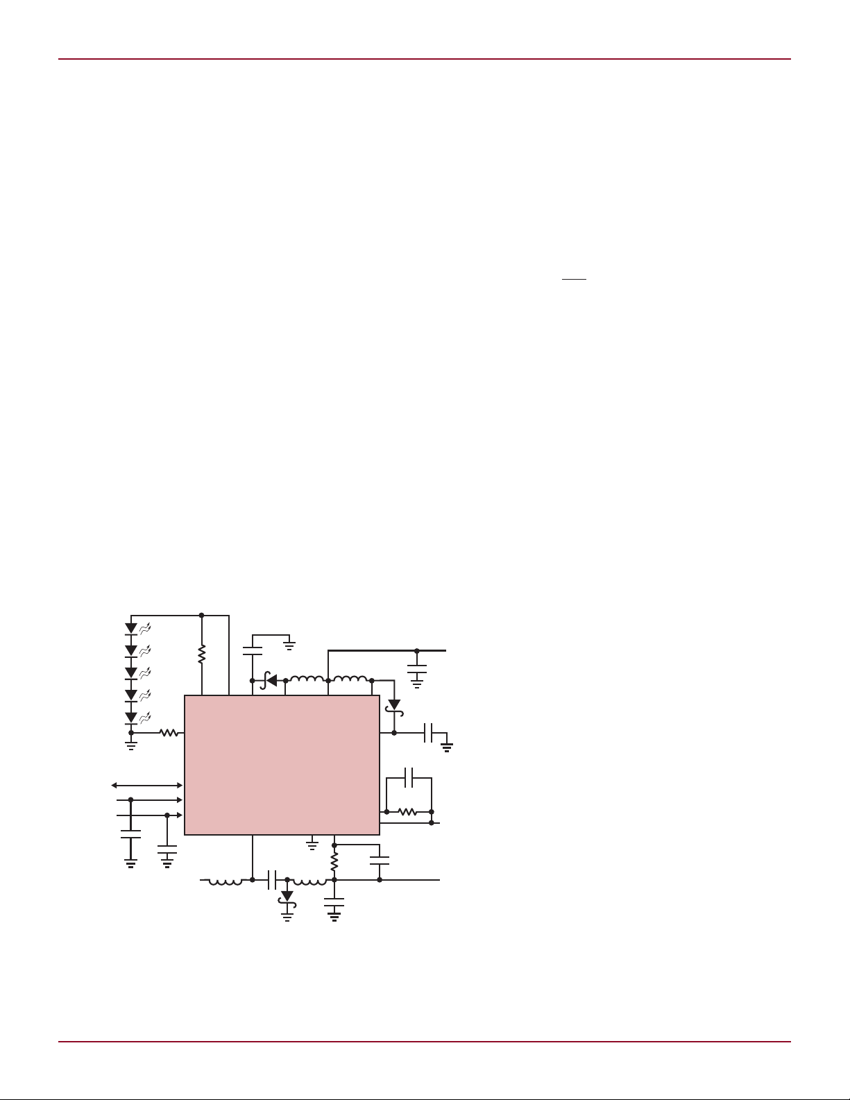
Figure 1. Solution for a Li-Ion powered camera provides positive and negative
supplies for biasing a CCD imager and an LED driver for a 5-LED backlight
Triple-Output Supply for CCD
Imager and LED Backlight
Figure 1 shows a typical application
providing a positive and negative voltage bias for a CCD imager and a 20mA
current bias for an LED backlight. All
three channels of the LT3587 use a
constant frequency, current mode control scheme to provide voltage and/or
current regulation at the output.
The positive CCD bias is configured as a simple non-synchronous
boost converter. Its output voltage is
set to 15V via the feedback resistor
R
. The 15µH inductor (L1) is sized
FB1
for a maximum load of 50mA. The
negative CCD bias is configured as a
non-synchronous ´Cuk converter. Its
output voltage is set at –8V using the
feedback resistor R
Linear Technology Magazine • January 2009
. The two 15µH
FB2
DISCONNECT
CONTROL
TO INTERNAL
CIRCUIT
LT3587
M2
M3
CAP3
V
OUT3
V
OUT1
CAP1
C1
C4
OVERVOLTAGE
PROTECTION
DISCONNECT
CONTROL
SHDN3
SHDN1
M1
I
FB3
R
IFB3
I
VIN
500mA/DIV
V
VOUT1
10V/DIV
V
NEG
10V/DIV
V
EN/SS1
2V/DIV
400µs/DIV
0V
0V
0V
0mA
I
VIN
500mA/DIV
V
VOUT1
10V/DIV
V
NEG
10V/DIV
V
EN/SS1
2V/DIV
4ms/DIV
0mA
0V
0V
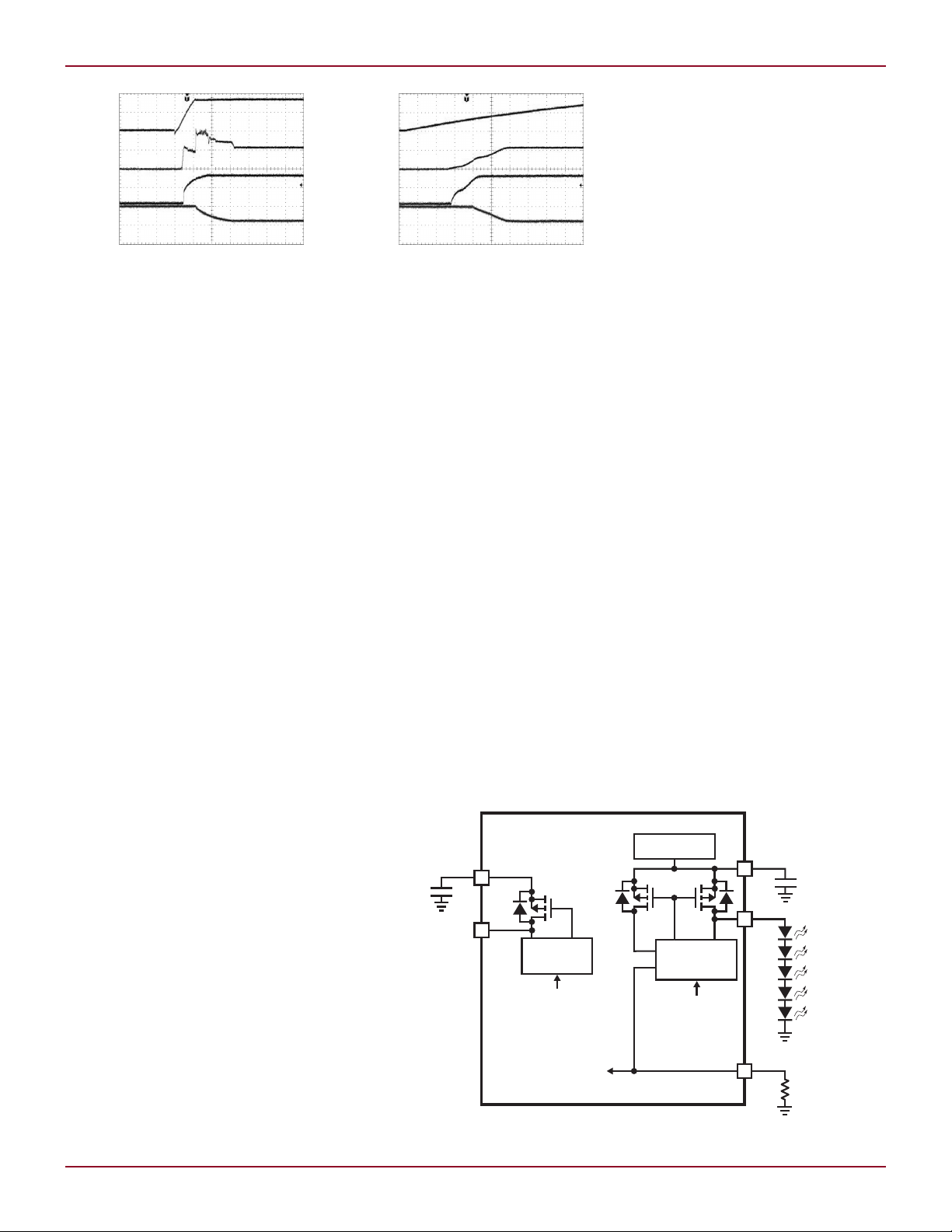
Figure 2. Start-up waveforms with no soft-start capacitor, and with a 10nF soft-start capacitor
(L2 and L3) inductors are sized for a
maximum load of 100mA.
The LED backlight driver is configured as an output-current-regulated
boost converter. Its output current is
set at 20mA using the current programming resistor R
. The 10µH
IFB3
inductor (L4) is sized for a typical load
of 20mA at up to 24V. Note the optional
voltage feedback resistor, R
VFB3
, on
the LED driver. This resistor acts as
a voltage clamp on the LED driver
output, so that if one of the LED fails
open, the voltage on the LED driver
output is clamped to 24V.
voltage on the EN/SS1 pin is at least
600mV. This ensures that channel 2
starts up after channel 1. Channel 1
and channel 2 regulation loops are
free running with full inductor current
when the voltage at the EN/SS1 pin
is above 2.5V.
In a similar fashion, a capacitor
from the EN/SS3 pin to ground (C5
in Figure 1) sets up a soft-start ramp
for channel 3. When the voltage at the
EN/SS3 pins goes above 200mV, regulation loop for channel 3 is enabled.
When the voltage at the EN/SS3 pin
is above 2V, the regulation loop for
channel 3 is free running with full
Soft-Start
inductor current.
All channels feature soft-start (a slow
voltage ramp from zero to regulation)
to prevent potentially damaging large
inrush currents at start-up. Softstart is implemented via two separate
soft-start control pins: EN/SS1 and
EN/SS3. The EN/SS1 pin controls
Start-Up Sequencing
The LT3587 also includes internal
sequencing circuitry that inhibits the
channel 2 from operating until the
feedback voltage of channel 1 (at the
FB1 pin) reaches about 1.1V (about
the soft-start for channel 1 and the
inverter, while the EN/SS3 pin controls
the soft-start for channel 3. Both of
these soft-start pins are pulled up with
a 1µA internal current source.
A capacitor from the EN/SS1 pin
to ground (C3 in Figure 1) programs
a soft-start ramp for channel 1 and
channel 2 (the inverter). As the 1µA
current source charges up the capacitor, the regulation loops for channel
1 and channel 2 are enabled when
the EN/SS1 pin voltage rises above
200mV. During start-up, the peak
switch current for channel 1 proportionally rises with the soft-start voltage
ramp at the EN/SS1 pin. The inverter
switch current also follows the voltage
ramp at the EN/SS1 pin, but its switch
current ramp does not start until the
Linear Technology Magazine • January 2009
Figure 3. Partial block diagram of the LT3587 showing the disconnect PMOS for channels 1 and 3
DESIGN FEATURES L
87% of the final voltage). The size of the
soft-start capacitor controls channel
2 start-up behavior.
If there is no soft-start capacitor,
or a very small capacitor, then the
negative channel starts up immediately with full inductor current when
the positive output reaches 87% of its
final value. If a large soft-start capacitor is used, then the EN/SS1 voltage
controls the inverter channel past
the point of regulation of the positive
channel. Figure 2 shows the start-up
sequencing without soft-start and with
a 10nF soft-start capacitor.
Output Disconnect
Both of the positive channels (channels
1 and 3) have an output disconnect
between their respective CAP and V
pins. This disconnect feature prevents
a DC path from forming between V
and V
through the inductors when
OUT
switching is disabled (Figure 1).
For channel 1, this output disconnect feature is implemented using a
PMOS (M1) as shown in the partial block
diagram in Figure 3. When turned on,
M1 normally provides a low resistance,
low power dissipation path for delivering output current between the CAP1
pin and the V
pin. M1 is on as long
OUT1
as the voltage difference between CAP1
and V
is greater than 2.5V. This al-
IN
lows the positive bias to stay high as
long as possible while the negative bias
discharges during turn off.
OUT
21
IN

L DESIGN FEATURES
I
L4
500mA/DIV
V
CAP3
10V/DIV
V
VOUT3
10V/DIV
I
VOUT3
500mA/DIV
40µs/DIV
0mA
24V
I
L4
500mA/DIV
V
CAP3
10V/DIV
V
VOUT3
10V/DIV
I
VOUT3
500mA/DIV
40µs/DIV
24V
0mA
V
VIN
= 3.6V
C4 = 1µF
I
L1
500mA/DIV
V
CAP1
10V/DIV
V
VOUT1
10V/DIV
I
VOUT1
500mA/DIV
40µs/DIV
V
VIN
= 3.6V
C1 = 4.7µF
0mA
15V
15V
ENSS1/ENSS3
5V/DIV
V
NEG
10V/DIV
V
VOUT3
20V/DIV
V
VOUT1
10V/DIV
V
FLT
5V/DIV
100ms/DIV
PART RESET
SHORT
AT V
OUT1
ENSS1/ENSS3
5V/DIV
V
NEG
10V/DIV
V
VOUT3
20V/DIV
V
VOUT1
10V/DIV
V
FLT
5V/DIV
100ms/DIV
PART RESET
FLT FORCED LOW
Figure 4. Channel 1 short circuit event
Figure 6. Fault detection
of a short circuit event
The disconnect transistor M1 is
current limited to provide a maximum
output current of 155mA. There is also
a protection circuit for M1 that limits
the voltage drop across CAP1 and
V
to about 10V. When the voltage
OUT1
at CAP1 is greater than 10V, such as
during an output overload or short
circuit to ground, then M1 is set fully
on, without any current limit, to allow
for the voltage on CAP1 to discharge
as fast as possible. When the voltage
across CAP1 and V
reduces to
OUT1
less than 10V, the output current is
then again limited to 155mA. Figure 4
shows the output voltage and current
during an overload event with V
initially at 15V.
The output disconnect feature on
channel 3 is implemented similarly
using M3 (Figure 3). However, in this
case M3 is only turned off when the
EN/SS3 pin voltage is less than 200mV
and the regulation loop for channel 3
is disabled.
The disconnect transistor M3 is also
current limited, providing a maximum
output current at V
also has a similar protection circuit as
of 100mA. M3
OUT3
M1 that limits the voltage drop across
CAP3 and V
22
to about 10V. Figure 5
OUT3
Figure 5. Channel 3 short circuit condition with and without 20mA current limit
Figure 7. Waveforms for when the
FLT pin is externally forced low
The LT3587 is a versatile,
highly integrated device
that provides a compact
solution for devices such
as cameras, handheld
computers and terminals
requiring multiple high
voltage supplies. A low part
count and a 3mm × 3mm
package keep the solution
size small. High efficiency
conversion makes it
CAP1
applications. Adjustable
suitable for battery powered
output voltage and wide
output range of up to 32V for
the positive boosts, and –32V
for the inverter, make it a
flexible solution for systems
that require high voltage
supplies.
shows the output voltage and current
during an overload event with V
initially at 24V.
Fault Detection and Indicator
The LT3587 features fault detection on
all outputs and a fault indicator pin,
FLT. The fault detection circuitry is
enabled only when at least one of the
channels has completed the soft-start
process and is free running with full
inductor current. Once fault detection is enabled, if any of the enabled
channel feedback voltages (V
or the greater of V
below its regulation value for more
than 16ms, the FLT pin pulls low.
One particularly important case is
an overload or short circuit condition
on any of the outputs. In this case, if
the corresponding loop is unable to
bring the output back into regulation
within 16ms, a fault is detected and
the FLT pin pulls low.
Note that the fault condition is
latched—once activated all three channels are disabled. Enabling any of the
channels requires resetting the part
by shutting it down (forcing both the
EN/SS1 and EN/SS3 pins low below
200mV) and then on again. Figure 6
shows the waveforms when a short
circuit condition occurs at channel 1
for more than 16ms and the subse-
CAP3
quent resetting of the part.
Linear Technology Magazine • January 2009
VFB3
and V
FB1
IFB3
, V
FB2
) falls

DESIGN FEATURES L
ENSS3
5V/DIV
I
L4
200mA/DIV
I
VOUT3
13mA/DIV
2ms/DIV
V
VIN
= 3.6V
6 LEDs
0mA
0mA
0V
PWM
FREQ
2.5V
0V
MN1
Si1304BDL
10µH
V
OUT3
CAP3
I
FB3
LT3587
R
IFB3
8.06k
EN/SS3
SW3
V
IN
LED DRIVER
1µF
V
VIN
2.5V TO 5V
10µH
V
OUT3
CAP3
I
FB3
LT3587
R
IFB3
8.06k
EN/SS3
SW3
V
IN
LED DRIVER
1µF
V
VIN
2.5V TO 5V
V
DAC-OUT
DAC
LTC2630
Figure 8. Analog dimming using a DAC and a resistor
Besides acting as a fault output
indicator, the FLT pin is also an input
pin. If this pin is externally forced
below 400mV, the LT3587 behaves
as if a fault event has occurred and
all the channels turn off. In order to
turn the part back on, remove the
external voltage that forces the pin low
and reset the part. Figure 7 shows the
waveforms when the FLT pin is externally forced low and the subsequent
resetting of the part.
Dimming Control for
Channel 3 as a CurrentRegulated LED Driver
As shown in Figure 1, one of the most
common applications for the channel
3 is as a current regulator for a backlight LED driver. In many high end
display applications requiring an LED
backlight, the ability to dim the display
brightness is crucial for implementing
a power saving mode or to maintain
contrast in different ambient lighting
conditions.
There are two different ways to
implement a dimming control of
the LED string. LED current can be
adjusted by either using a digital to
analog converter (DAC) and a resistor
R
IFB3
Analog Dimming Using
a DAC and a Resistor
For some applications, the preferred
method of brightness control is using
a DAC and a resistor. This method
Linear Technology Magazine • January 2009
or by using a PWM signal.
Figure 9. Driver for six LEDs with PWM dimming
is more commonly known as analog
dimming. This method is shown in
Figure 8.
Since the programmed V
OUT3
cur -
rent is proportional to the current
through R
, the LED current can be
IFB3
adjusted by changing the DAC output
voltage. A higher DAC output voltage
level results in lower LED current and
hence lower overall brightness. For
accurate dimming control, keep the
DAC output impedance low enough
to sink approximately 1/200 of the
desired maximum LED current. Note
the maximum possible output current
is limited by the output disconnect
current limit to 100mA.
PWM Dimming
One problem with analog dimming as
described above is that changing the
forward current flowing in the LEDs
not only changes the brightness intensity of the LEDs, it also changes the
color. This is a problem for applications
Figure 10. PWM dimming waveforms
that cannot tolerate any shift in the
LED chromaticity.
Controlling the LED intensity with
a direct PWM signal allows dimming
of the LEDs without changing the
color. A PWM frequency of ~80Hz or
higher guarantees that there is no
visible flicker. The amount of on-time
in the PWM signal is proportional to
the intensity of the LEDs. The color of
the LEDs remains unchanged in this
scheme since the LED current value is
either zero or a constant value (I
= 160V/R
IFB3
).
VOUT3
Figure 9 shows an LED driver for
six white LEDs. If the voltage at the
CAP3 pin is higher than 10V when
the LED is on, direct PWM dimming
method requires an external NMOS.
This external NMOS is tied between
the cathode of the lowest LED in the
string and ground.
The output disconnect feature
and the external NMOS ensure that
the LEDs quickly turn off without
discharging the output capacitor.
This allows the LEDs to turn on
faster. Figure 10 shows the PWM
dimming waveforms for the circuit in
Figure 9.
The time it takes for the LED current
to reach its programmed value sets the
achievable dimming range for a given
PWM frequency. At extreme lower end
of the duty cycle, the linear relation
between the average LED current
and the PWM duty cycle is no longer
preserved. The minimum on time is
23

L DESIGN FEATURES
V
VIN
= 3.6V
WITHOUT PROGRAMMED OUTPUT VOLTAGE
CLAMP: V
FB3
CONNECTED TO GND
I
L4
200mA/DIV
V
VOUT3
10V/DIV
200µs/DIV
20V
OUTPUT LOAD
DISCONNECTED
V
VIN
= 3.6V
WITH PROGRAMMED OUTPUT
VOLTAGE CLAMP AT 24V
I
L4
200mA/DIV
V
VOUT3
10V/DIV
200µs/DIV
20V
OUTPUT LOAD
DISCONNECTED
V
VIN
= 3.6V
WITHOUT CURRENT LIMIT: I
FB3
CONNECTED TO GND
V
OUT3
STAYS AT 15V, OUTPUT CURRENT
INCREASES FROM 20mA TO 40mA
I
L4
200mA/DIV
V
VOUT3
5V/DIV
I
VOUT3
13mA/DIV
200µs/DIV
15V
20mA
LOAD STEP
V
VIN
= 3.6V
WITH 20mA CURRENT LIMIT: R
IFB3
= 8.06k
OUTPUT CURRENT STAYS AT 20mA,
V
OUT3
DROPS FROM 15V TO 7.5V
I
L4
200mA/DIV
V
VOUT3
5V/DIV
I
VOUT3
13mA/DIV
200µs/DIV
15V
20mA
LOAD STEP
chosen based on how much linearity
is required for the average LED current. For example for the circuit in
Figure 9, to produce approximately
10% deviation from linearity at the
lower duty cycle, the minimum on
time of the LED current is approximately 320µs (3.2% duty cycle) for a
3.6V input voltage and a 100Hz PWM
frequency. The achievable dimming
range for this application is then 30
to 1 (approximately the reciprocal of
the minimum duty cycle).
The dimming range can be significantly extended by combining PWM
dimming with analog dimming. The
color of the LEDs no longer remains
constant because the forward current
of the LED changes with the output
voltage of the DAC. For the six LED
application described above, the LEDs
can be dimmed first by modulating the
duty cycle of the PWM signal with the
DAC output at 0V. Once the minimum
duty cycle is reached, the value of the
DAC output voltage can be increased
to further dim the LEDs. The use of
both techniques together allows the
average LED current for the six LED
application to be varied from 20mA
down to less than 1µA (a 20000:1
dimming ratio).
Channel 3 can be configured
either as a voltage-regulated
boost converter or as a
current-regulated boost
converter. The regulation
loop of channel 3 uses the
greater of the two voltages
at V
FB3
and I
as feedback
FB3
to set the peak current
of its power switch. This
architecture allows for a
programmable current limit
on voltage regulation or a
voltage limit on
current regulation.
the V
load current is less than I
3 regulates the voltage at the V
to 0.8V. If there is an increase in load
current beyond I
V
FB3
I
FB3
loop then regulates the voltage at the
I
FB3
pin. In this case, when the
OUT3
, the voltage at
LIMIT
, channel
LIMIT
FB3
pin
starts to drop and the voltage at
rises above 0.8V. The channel 3
pin to 0.8V, limiting the output
current at V
OUT3
to I
. Figure 11
LIMIT
compares the transient responses
with and without current limit when
a current overload occurs.
The channel 3 CAP3 pin has over
voltage protection. When the voltage at
CAP3 is driven above 29V, the channel 3 loop is disabled and SW3 pin
stops switching. When configured as
a boost current regulator, a feedback
resistor from the I
sets the output current at V
a fixed level. In this case, if the V
pin to ground
FB3
OUT3
at
FB3
pin is grounded then the over voltage
protection defaults to 29V.
On the other hand a resistor can
be connected from the V
the V
clamp (V
pin to set an output voltage
FB3
) level lower than 29V.
CLAMP
OUT3
pin to
In this case, when the voltage level is
less than V
regulates the voltage at the I
the channel 3 loop
CLAMP
,
FB3
pin
to 0.8V. On the other hand, when
the output load fails open circuit or
disconnected, the voltage at I
FB3
drops
to reflect the lower output current
and the voltage at V
When the voltage at V
V
, the voltage at the V
CLAMP
starts to rise.
FB3
rises beyond
OUT3
pin goes
FB3
Channel 3 Overvoltage and
Overcurrent Protection
Channel 3 can be configured either as
a voltage regulated boost converter or
as a current regulated boost converter.
The regulation loop of channel 3 uses
the greater of the two voltages at V
and I
current of its power switch. This architecture allows for a programmable
current limit on voltage regulation or
voltage limit on current regulation.
age regulator, a feedback resistor
from the output pin V
pin sets the voltage level at V
a fixed level. In this case, the I
can either be grounded if no current
limiting is desired or be connected to
ground with a resistor to set an output
current limit value (I
noted before, the pull up current on
the I
1/200 of the output load current at
as feedback to set the peak
FB3
When configured as a boost volt-
to the V
OUT3
pin is controlled to be typically
FB3
). As briefly
LIMIT
OUT3
pin
FB3
FB3
Figure 11. Channel 3 in an output current overload event with and without output current limit
FB3
at
Figure 12. Channel 3 in an output open circuit with
and without programmed output voltage clamp
24
Linear Technology Magazine • January 2009

DESIGN FEATURES L
L1
15µH
L4
10µH
V
OUT3
CAP3
V
FB3
I
FB3
SW2
GND
FB2
CAP1
FB1
V
OUT1
LT3587
FLT
EN/SS1
EN/SS3
SW3 SW1V
IN
C6
1µF
CCD POSITIVE
15V
50mA
V
VIN
2.5V TO 6V
C2
2.2µF
D3
R
FB2
1M
CCD NEGATIVE
–8V
100mA
R
IFB3
7.15k
(OPTIONAL)
C4
1µF
OLED DRIVER
16V
20mA
V
VIN
2.5V TO 6V
C7
22µF
D
S1
C1
4.7µF
R
FB1
1M
D
S3
C5
100nF
C
FB2
6.8pF
C3
100nF
D
S2
L2
15µH
C1: TAIYO YUDEN TMK212BJ475KG-T
C2: TAIYO YUDEN EMK107BJ225KA-T
C3, C5: TAIYO YUDEN JMK063BJ104KP-F
C4: TAIYO YUDEN GMK107BJ105KA-T
C6: TAIYO YUDEN LMK105BJ105KV-F
C7: TAIYO YUDEN LMK212BJ226MG-T
C
FB1
: TAIYO YUDEN EMK105SK2R7JW-F
C
FB2
: TAIYO YUDEN EMK105SH6R8JW-F
L1, L2: SUMIDA CDRH2D18/HP-150N
L4: TOKO 1071AS-100M
DS1, DS2, DS3, D3: NXP PMEG2005EB
R
VFB3
1.07M
C
FB1
2.7pF
L1
15µH
L4
10µH
I
FB3
EN/SS3
EN/SS1
FLT
SW2 GND FB2
CAP1
FB1
V
OUT1
LT3587
V
FB3VOUT3
CAP3 SW3 SW1
C1
4.7µF
R
FB1
787k
2AA CELLS
2V TO 3.2V
C2
2.2µF
L2
15µH
L3
15µH
R
FB2
1M
LED DRIVER
20mA UP TO 12V
2AA CELLS
2V TO 3.2V
C7
10µF
D
S2
V
IN
D
S3
C4
1µF
R
VFB3
787k
(OPTIONAL)
D
S1
R
IFB3
8.06k
C1: MURATA GRM21BR61E475KA12L
C2: MURATA GRM188R61C225KE15D
C4: MURATA GRM188R61E105KA12B
C6: MURATA GRM155R61A105KE15D
C7: MURATA GRM21BR71A106KE51L
C
FB1
: MURATA GRM1555C1H3R3BZ01D
C
FB2
: MURATA GRM1555C1H6R3BZ01D
L1, L2, L3: SUMIDA CDRH2D18/HP-150N
L4: TOKO 1071AS-100M
DS1, DS2, DS3: NXP PMEG2005EB
C6
1µF
3.3V
C
FB1
3.3pF
C
FB2
6.8pF
CCD POSITIVE
15V
10mA
CCD NEGATIVE
–8V
20mA
above 0.8V. The channel 3 loop then
regulates the voltage at the V
FB3
pin
to 0.8V, limiting the voltage level at
V
OUT3
to V
. Figure 12 contrasts
CLAMP
the transient responses with and
without programmed V
CLAMP
when the
output load is disconnected.
Low Input Voltage
While the LT3587’s V
range is 2.5V to 6.0V, the inductors can
run off a lower voltage. Most portable
devices and systems have a separate
3.3V logic supply voltage, which can
be used to power the LT3587. This
allows the outputs to be powered
straight from the lower voltage power
source such as two alkaline cells.
This configuration results in higher
efficiency. Figure 13 shows a typical
digital still camera application powered
this way. It has positive and negative
CCD supplies and an LED backlight
supply.
supply voltage
IN
Adjustable output voltage and wide
output range of up to 32V for the positive boosts, and –32V for the inverter,
make it a flexible solution for systems
that require high voltage supplies.
Channel 3’s ability to work as a voltage
regulator or as a true 1-wire current
regulator give the LT3587 status as a
true all-in-one power supply.
Additional features, such as softstart, supply sequencing, output
disconnect and fault handling also add
to the versatility of this part and further
simplify power supply design.
L
Replace Inductor
with Schottky for
Smaller Footprint
If higher current ripple is tolerable at
the output of the inverter (channel 2),
replace inductor L3 with a Schottky
diode D3 as shown in Figure 14.
Since the Schottky diode footprint
is usually smaller than the inductor
footprint, this alternate topology is
recommended for space constrained
applications. This topology is only
viable if the absolute value of the inverter output is greater than V
Schottky diode is configured with the
anode connected to the output of the
inverter and the cathode to the output
end of the flying capacitor C2 as shown
in Figure 14.
Conclusion
The LT3587 is a versatile, highly integrated device that provides a simple
solution to devices such as cameras,
handheld computers and terminals
requiring multiple high voltage supplies. A low part count and a compact
3mm × 3mm package keep the solution
size small. High efficiency conversion
makes it suitable for battery powered
applications.
Linear Technology Magazine • January 2009
IN
. This
Figure 13. Two AA cells produce CCD positive and
negative supplies and a driver for a 3-LED backlight.
Figure 14. Li-ion driver for an OLED panel and a CCD imager
with a Schottky diode replacing the inverter’s output inductor
25
 Loading...